EP1965434A2 - Dispositif de semi-conducteur à composant et amplificateur Doherty utilisant un dispositif de semi-conducteur à composant - Google Patents
Dispositif de semi-conducteur à composant et amplificateur Doherty utilisant un dispositif de semi-conducteur à composant Download PDFInfo
- Publication number
- EP1965434A2 EP1965434A2 EP20080101728 EP08101728A EP1965434A2 EP 1965434 A2 EP1965434 A2 EP 1965434A2 EP 20080101728 EP20080101728 EP 20080101728 EP 08101728 A EP08101728 A EP 08101728A EP 1965434 A2 EP1965434 A2 EP 1965434A2
- Authority
- EP
- European Patent Office
- Prior art keywords
- transport layer
- electron transport
- compound semiconductor
- electron
- supply layer
- Prior art date
- Legal status (The legal status is an assumption and is not a legal conclusion. Google has not performed a legal analysis and makes no representation as to the accuracy of the status listed.)
- Granted
Links
Images



Classifications
-
- H—ELECTRICITY
- H10—SEMICONDUCTOR DEVICES; ELECTRIC SOLID-STATE DEVICES NOT OTHERWISE PROVIDED FOR
- H10D—INORGANIC ELECTRIC SEMICONDUCTOR DEVICES
- H10D30/00—Field-effect transistors [FET]
- H10D30/40—FETs having zero-dimensional [0D], one-dimensional [1D] or two-dimensional [2D] charge carrier gas channels
- H10D30/47—FETs having zero-dimensional [0D], one-dimensional [1D] or two-dimensional [2D] charge carrier gas channels having two-dimensional [2D] charge carrier gas channels, e.g. nanoribbon FETs or high electron mobility transistors [HEMT]
- H10D30/471—High electron mobility transistors [HEMT] or high hole mobility transistors [HHMT]
- H10D30/473—High electron mobility transistors [HEMT] or high hole mobility transistors [HHMT] having confinement of carriers by multiple heterojunctions, e.g. quantum well HEMT
- H10D30/4732—High electron mobility transistors [HEMT] or high hole mobility transistors [HHMT] having confinement of carriers by multiple heterojunctions, e.g. quantum well HEMT using Group III-V semiconductor material
- H10D30/4738—High electron mobility transistors [HEMT] or high hole mobility transistors [HHMT] having confinement of carriers by multiple heterojunctions, e.g. quantum well HEMT using Group III-V semiconductor material having multiple donor layers
-
- H—ELECTRICITY
- H10—SEMICONDUCTOR DEVICES; ELECTRIC SOLID-STATE DEVICES NOT OTHERWISE PROVIDED FOR
- H10P—GENERIC PROCESSES OR APPARATUS FOR THE MANUFACTURE OR TREATMENT OF DEVICES COVERED BY CLASS H10
- H10P10/00—Bonding of wafers, substrates or parts of devices
-
- H—ELECTRICITY
- H03—ELECTRONIC CIRCUITRY
- H03F—AMPLIFIERS
- H03F1/00—Details of amplifiers with only discharge tubes, only semiconductor devices or only unspecified devices as amplifying elements
- H03F1/02—Modifications of amplifiers to raise the efficiency, e.g. gliding Class A stages, use of an auxiliary oscillation
- H03F1/0205—Modifications of amplifiers to raise the efficiency, e.g. gliding Class A stages, use of an auxiliary oscillation in transistor amplifiers
- H03F1/0288—Modifications of amplifiers to raise the efficiency, e.g. gliding Class A stages, use of an auxiliary oscillation in transistor amplifiers using a main and one or several auxiliary peaking amplifiers whereby the load is connected to the main amplifier using an impedance inverter, e.g. Doherty amplifiers
-
- H—ELECTRICITY
- H03—ELECTRONIC CIRCUITRY
- H03F—AMPLIFIERS
- H03F1/00—Details of amplifiers with only discharge tubes, only semiconductor devices or only unspecified devices as amplifying elements
- H03F1/02—Modifications of amplifiers to raise the efficiency, e.g. gliding Class A stages, use of an auxiliary oscillation
- H03F1/04—Modifications of amplifiers to raise the efficiency, e.g. gliding Class A stages, use of an auxiliary oscillation in discharge-tube amplifiers
- H03F1/06—Modifications of amplifiers to raise the efficiency, e.g. gliding Class A stages, use of an auxiliary oscillation in discharge-tube amplifiers to raise the efficiency of amplifying modulated radio frequency waves; to raise the efficiency of amplifiers acting also as modulators
- H03F1/07—Doherty-type amplifiers
-
- H—ELECTRICITY
- H10—SEMICONDUCTOR DEVICES; ELECTRIC SOLID-STATE DEVICES NOT OTHERWISE PROVIDED FOR
- H10D—INORGANIC ELECTRIC SEMICONDUCTOR DEVICES
- H10D30/00—Field-effect transistors [FET]
- H10D30/01—Manufacture or treatment
- H10D30/015—Manufacture or treatment of FETs having heterojunction interface channels or heterojunction gate electrodes, e.g. HEMT
-
- H—ELECTRICITY
- H10—SEMICONDUCTOR DEVICES; ELECTRIC SOLID-STATE DEVICES NOT OTHERWISE PROVIDED FOR
- H10D—INORGANIC ELECTRIC SEMICONDUCTOR DEVICES
- H10D62/00—Semiconductor bodies, or regions thereof, of devices having potential barriers
- H10D62/80—Semiconductor bodies, or regions thereof, of devices having potential barriers characterised by the materials
- H10D62/85—Semiconductor bodies, or regions thereof, of devices having potential barriers characterised by the materials being Group III-V materials, e.g. GaAs
-
- H—ELECTRICITY
- H10—SEMICONDUCTOR DEVICES; ELECTRIC SOLID-STATE DEVICES NOT OTHERWISE PROVIDED FOR
- H10D—INORGANIC ELECTRIC SEMICONDUCTOR DEVICES
- H10D62/00—Semiconductor bodies, or regions thereof, of devices having potential barriers
- H10D62/80—Semiconductor bodies, or regions thereof, of devices having potential barriers characterised by the materials
- H10D62/85—Semiconductor bodies, or regions thereof, of devices having potential barriers characterised by the materials being Group III-V materials, e.g. GaAs
- H10D62/8503—Nitride Group III-V materials, e.g. AlN or GaN
-
- H—ELECTRICITY
- H10—SEMICONDUCTOR DEVICES; ELECTRIC SOLID-STATE DEVICES NOT OTHERWISE PROVIDED FOR
- H10D—INORGANIC ELECTRIC SEMICONDUCTOR DEVICES
- H10D64/00—Electrodes of devices having potential barriers
- H10D64/60—Electrodes characterised by their materials
- H10D64/62—Electrodes ohmically coupled to a semiconductor
Definitions
- the present invention relates to a compound semiconductor device and a Doherty amplifier using the compound semiconductor device, and more particularly to a Doherty amplifier using field effect transistors, and a compound semiconductor device applicable to a peak amplifier of the Doherty amplifier.
- GaN has a band gap of 3.4 eV and is expected to operate at higher breakdown voltage than GaAs having a band gap of 1.4 eV. If a high electron mobility transistor (HEMT) made of GaN and having a high breakdown voltage is used as an amplifier, this amplifier can operate along a load line corresponding to large load impedance on a graph showing current-voltage characteristic. A high efficiency operation is therefore possible.
- HEMT high electron mobility transistor
- a base station amplifier for world interoperability for microwave access requires a nonconventional high efficiency.
- WiMAX world interoperability for microwave access
- Fig. 1 is a fundamental equivalent circuit diagram of a Doherty amplifier.
- a high frequency signal input from an input terminal Ti is divided into two parts. One part is input to a carrier (main) amplifier 100 and the other part is input to a peak (auxiliary) amplifier 101 via a quarter-wave line 103. Another quarter-wave line 102 is connected to an output terminal of the carrier amplifier 100. An output signal of the carrier amplifier 100 passes through the quarter-wave line 102 and thereafter is combined with an output signal of the peak amplifier 101.
- a load impedance R L is connected to an output terminal To.
- the carrier amplifier 100 is biased to operate as class A or class AB, and the peak amplifier 101 is biased so that an idle current is smaller than that of the carrier amplifier 100.
- Fig. 9 shows an example of input/output characteristics of a Doherty amplifier.
- a solid line ac and a broken line ap0 indicate the input/output characteristics of the carrier amplifier 100 and peak amplifier 101, respectively.
- a solid line at indicates the input-output characteristics of the Doherty amplifier including the carrier amplifier 100 and peak amplifier 101.
- the carrier amplifier 100 When an input power is small and the Doherty amplifier operates in the back-off region, mainly the carrier amplifier 100 operates and outputs an output signal. When the input power is sufficiently large and an output power of the carrier amplifier 100 saturates, the peak amplifier 101 operates and outputs an output signal. During the operation in the back-off region, a d.c. consumption power of the peak amplifier 101 is sufficiently small. An efficiency of the Doherty amplifier itself is therefore high. Since output signals of the carrier amplifier 100 and peak amplifier 101 are combined, a large output power can be obtained.
- a compound semiconductor device including:
- a Doherty amplifier using the above-described compound semiconductor device as the peak amplifier.
- Fig. 1 is an equivalent circuit diagram of a Doherty amplifier according to the first embodiment. Since the fundamental structure has already been described, redundant description is avoided here.
- Each of the carrier amplifier 100 and peak amplifier 101 includes a HEMT using GaN as the material of an electron transport layer.
- Bias circuits 104 and 105 apply a d.c. gate bias voltage to respective gates of HEMT's constituting the carrier amplifier 100 and peak amplifier 101.
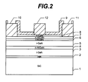
- Fig. 2 is a cross sectional view of the HEMT to be applied to the peak amplifier 101.
- An underlie (underlying) layer 2 made of AIN and having a thickness of 0.3 ⁇ m is formed on a substrate 1 made of single crystal SiC.
- a lower electron transport layer 3 a lower electron supply layer 4
- an upper electron transport layer 5 a non-doped layer 6 and an upper electron supply layer 7 are stacked in this order.
- the lower electron transport layer 3 is made of non-doped GaN and has a thickness of 3 ⁇ m.
- the lower electron supply layer 4 is made of compound semiconductor material having smaller electron affinity than that of the lower electron transport layer 3, for example, n-type AlGaN doped with Si only at 2 x 10 18 cm -3 .
- the lower electron supply layer 3 has a thickness of 20 nm.
- An atomic ratio Al/(group III element) in a region that is in contact with the lower electron transport layer 3 is 0.05.
- the atomic ratio Al/(group III element) becomes lower toward a shallow region, and a region that is in contact with the upper electron transport layer 5 has an atomic ratio Al/(group III element) of 0.02.
- the upper electron transport layer 5 is made of non-doped GaN and has a thickness of 50 nm.
- the non-doped layer 6 is made of non-doped Al 0.25 Ga 0.75 N and has a thickness of 5 nm.
- the upper electron supply layer 7 is made of compound semiconductor material having a smaller electron affinity than that of the upper electron transport layer 5, for example, n-type Al 0.25 Ga 0.75 N doped with Si at 4 x10 18 cm -3 .
- the upper electron supply layer has a thickness of 20 nm.
- a source electrode 10 and a drain electrode 11 are disposed at a distance from each other on partial surfaces of the upper electron supply layer 7.
- Each of the source electrode 10 and the drain electrode 11 has a laminated structure having a Ta layer in contact with the upper electron supply layer 7 and an Al layer formed on the Ta layer, and is in ohmic contact with the lower and upper electron transport layers 3 and 5.
- a TaAl 3 layer is formed between the Ta layer and Al layer by mutual diffusion.
- the surface of the upper electron supply layer 7 between the source electrode 10 and drain electrode 11 is covered with a protective layer 8.
- the protective layer 8 is made of n-type GaN doped with Si at 5 x 10 18 cm -3 , and has a thickness of 7 nm.
- a gate electrode 12 is formed on a partial surface of the protecting layer 8 at a distance from both the source electrode 10 and drain electrode 11.
- the gate electrode 12 has a two-layer structure of a Ni layer in contact with the protective layer 8 and an Au layer formed on the Ni layer.
- a gate length (a lateral size of the gate electrode 12 in Fig. 2 ) is set to 0.5 ⁇ m, and a unit gate width is set to 300 ⁇ m.
- the "unit gate width" means a width of a region in which the gate electrode can control a density of two-dimensional electron gas.
- An insulating layer 9 covers the surfaces of the protective layer 8 between the gate electrode 12 and source electrode 10 and between the gate electrode 12 and drain electrode 11.
- the insulating layer 9 is made of SiN.
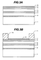
- each layer between the underlie layer 2 and the protective layer 8 is grown on the substrate 1 made of single crystal SiC, by metal organic vapor phase epitaxy (MOVPE).
- MOVPE metal organic vapor phase epitaxy
- trimethylaluminum is used as Al source material
- trimethylgallium is used as Ga source material
- ammonia is used as N source material
- silane is used as Si dopant source material.
- a resist film is formed on the protective layer 8.
- the resist film is exposed and developed to form openings corresponding to the source electrode 10 and drain electrode 11.
- a Ta film having a thickness of 10 nm and an Al film having a thickness of 280 nm are deposited on the whole surface of the substrate by vapor deposition.
- the resist film is removed together with the Ta film and Al film in the region other than the region of the source electrode 10 and drain electrode 11.
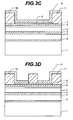
- the insulating film 9 of SiN is formed on the whole substrate surface by plasma enhanced chemical vapor deposition (PE-CVD).
- PE-CVD plasma enhanced chemical vapor deposition
- a resist film is formed on the insulating film 9.
- the resist film is exposed and deposited to form an opening corresponding to the gate electrode 12.
- a Ni film having a thickness of 10 nm and an Au film having a thickness of 200 nm are sequentially deposited on the whole substrate surface.
- the resist film together with the Ni film and Au film deposited thereon is removed.
- the gate electrode 12 is formed having a two-layer structure of the Ni film and Au film.
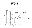
- Fig. 4 shows an energy band diagram of the HEMT shown in Fig. 2 .
- the abscissa represents the depth direction of each layer of the HEMT, and the ordinate represents a potential of electrons.
- a curve in Fig. 4 shows a potential at the lower end of a conduction band.
- a one-dot chain line Ef indicates a Fermi level. Piezo charges due to lattice mismatch are accumulated at an interface between the upper electron supply layer 7 and protective layer 8, at an interface between the upper electron transport layer 5 and non-doped layer 6 and at an interface between the lower electron transport layer 3 and lower electron supply layer 4. Therefore, slopes at the conduction band lower end are not the same on both sides of each of these interfaces.
- a two-dimensional electron gas density of the lower channel CH1 is at most 5 % of that of the upper channel CH0.
- a two-dimensional electron gas mobility of the lower channel CH1 is larger than 1000 cm/Vs.
- Fig. 5 shows an example of gate voltage (Vg) - drain current (Id) characteristics of the HEMT of the first embodiment shown in Fig. 2 .
- the abscissa represents a gate voltage Vg in the unit of "V", and the ordinate represents a drain current ld in an arbitrary unit.
- a bold line cp in Fig. 5 shows the characteristics of the HEMT shown in Fig. 2 .
- a narrow line cc is shown which indicates the characteristics of a general HEMT (hereinafter called "comparative example HEMT") in which the lower electron supply layer 4 and upper electron transport layer 5 are not disposed and the lower electron transport layer 3 is in contact with the non-doped layer 6.
- a channel consisting of two-dimensional electron gas is generated at an interface between the lower electron transport layer 3 and non-doped layer 6.
- a gate length was set to 0.8 ⁇ m and a unit gate width was set to 400 ⁇ m.
- the gate voltage Vg is changed gradually from a large negative voltage close to 0.
- the lower channel CH1 shown in Fig. 3 is generated and the drain current ld starts flowing.
- the drain current ld saturates once.
- the upper channel CH0 is generated so that as the gate voltage Vg increases, the drain current ld also increases.
- the gate voltage Vg is shown in the range of up to - 1 V in Fig. 5 , if the gate voltage Vg further increases, the drain current saturates eventually.
- a slope of the graph in the range of the gate voltage Vg between - 1.6 V and - 1 V is steeper than that in the range of the gate voltage Vg not higher than - 1.6 V.
- a drain current ld hardly flows until the gate voltage Vg reaches about - 1.6 V as indicated by the curve cc .
- the drain current Id also increases, as in the case of the HEMT of the first embodiment.
- the graph of the gate voltage - drain current characteristics has a shape with an extended gentle skirt.
- a gate bias voltage Vgp is set so that a drain current la at no a.c. input voltage (idle current) is smaller than the saturation current induced by the lower channel CH1.
- a drain current ld flows, substantially only through the lower channel CH1, and an output signal Wp0 is obtained.
- a gate bias voltage Vgc corresponding to the idle current la is higher than the gate bias voltage Vgp.
- a signal Wci having the same amplitude as that of the input signal Wpi is input, an output signal Wco is obtained. Since the slope of the curve cc near at the gate bias voltage Vgc is steeper than that of the curve cp near at the gate bias voltage Vgp, an amplitude of the output signal Wco is larger than that of the output signal Wpo, and the d.c. component of the drain current Id becomes large. Therefore, the d.c. component of the output power is large, and the efficiency is low.
- the amplitude of an output signal is small at a small input signal amplitude, it is possible to lower a gain and suppress an increase in the d.c. component of an output power.
- the gate bias voltage in such a manner that the HEMT applied to the peak amplifier operates in the skirt region of the gate voltage - drain current characteristics while an input signal amplitude is small. More specifically, it is preferable to set the gate bias voltage to such a value that the lower channel CH1 of two-dimensional electron gas is generated in the lower electron transport layer 3, but the upper channel CH0 is not generated in the upper electron transport layer 5.
- a difference between a gate voltage at which the drain current is 5 % of the saturation value and a gate voltage at which the drain current is 1 % of the saturation value is at least 0.5 V.
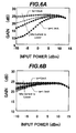
- Fig. 6A shows the relation between a gain and an input power of the HEMT of the first embodiment in respect of five values of idle current.
- Fig. 6B shows the relation between a gain and an input power of the comparative example HEMT in respect of eight values of idle current.
- the abscissa represents an input power in the unit of "dBm”
- the ordinate represents a gain in the unit of "dB”.
- the idle current was changed from 13 mA to 4.1 mA in five stages
- the comparative example shown in Fig. 6B the idle current was changed from 13 mA to 1.5 mA in eight stages.
- the gain is lowered considerably as the input power decreases. This is because when the idle current is made small, the HEMT operates in the region where the slope of the gate voltage - drain current characteristics cp shown in Fig. 5 is gentle.
- the gain reaches maximum (about 24 dB) at an input power of about 10 dBm, and the gain declines to 9 dB at an input power of - 10 dBm.
- a gain difference is about 15 dB.
- the solid line ap indicates the input/output characteristics of the peak amplifier including the HEMT of the first embodiment
- the broken line ap0 indicates the input/output characteristics of the peak amplifier including the comparative example HEMT.
- an output power of the peak amplifier including the HEMT of the first embodiment is smaller than that of the peak amplifier including the comparative example HEMT. This is because a gain at a small input power can be suppressed, as described with reference to Fig. 6A .
- an output of the peak amplifier at a small input power can be suppressed. Namely, an increase in the d.c. component of an output power can be suppressed. It is therefore possible to improve an efficiency of the Doherty amplifier itself.
- a distortion compensating circuit is generally combined with the amplifier to reduce leakage power to adjacent channels.
- a digital pre-distortion (DPD) has been adopted, in which distortion is compensated by applying in advance a signal having inverse characteristics of distortion to be generated.
- the carrier amplifier frequently operates in the saturation region. Therefore, since a large positive voltage is applied to the gate electrode, gate leak current is likely to increase. An increase in the gate leak current may cause collapse of distortion compensation. If an output power exceeds some level, the distortion compensation collapses.
- a Doherty amplifier using the conventional HEMT for each of the carrier amplifier and peak amplifier had an efficiency of 35 % at a distortion compensation collapse point, whereas a Doherty amplifier using the HEMT of the first embodiment for the peak amplifier had an efficiency of 42 % at a distortion compensation collapse point.
- An efficiency of a Doherty amplifier can thus be improved by using the HEMT of the first embodiment as the peak amplifier of the Doherty amplifier.
- an atomic ratio Al/(group III element) at the bottom of the lower electron supply layer 4 it is preferable to set an atomic ratio Al/(group III element) at the bottom of the lower electron supply layer 4 to a range between 0.03 and 0.07.
- the atomic ratio Al/(group III element) is made small, a density of two-dimensional electron gas in the lower channel CH1 becomes low, whereas as the atomic ratio Al/(group III element) is made large, the density of two-dimensional electron gas becomes high. If the density of two-dimensional gas in the lower channel CH1 becomes too low, the lower channel CH1 is not generated substantially.
- the saturation drain current induced by the lower channel CH1 shown in Fig. 5 becomes large, and a flat region in the skirt region of the curve cp becomes long. In this case, the efficiency lowers because a pinch-off current is likely to flow in the high drain voltage region during gate-off.
- An atomic ratio Al/(group III element) at the upper surface of the lower electron supply layer 4 is preferable set to a range between 0 and 0.03. As the atomic ratio Al/(group III element) becomes large, lattice mismatch becomes large at the interface between the upper electron transport layer 5 and lower electron supply layer 4, and piezo charges accumulate so that a level at the lower end of the conduction band of the energy band diagram is raised.
- a concentration of n-type dopant of the lower electron supply layer 4 is preferably set to a range between 1 x 10 17 cm -3 and 5 x 10 18 cm -3 , and more preferable to a range between 5 x 10 17 cm -3 and 2 x 10 18 cm -3 . If a concentration of n-type dopant is too low, an electron density lowers so that sufficient electrons cannot be supplied to the lower channel CH1. Conversely, if the concentration of n-type dopant is made high, a density of free electrons in the lower electron supply layer 4 becomes high. Free electrons in the lower electron supply layer 4 have a mobility lower than that of electrons accumulated in the lower channel CH1, and negatively affect the operation of the HEMT. Further, electrical isolation between the source and drain electrodes becomes insufficient.
- a concentration of n-type dopant of the upper electron transport layer 5 is preferably set to a range between 0 and 5 x 10 17 cm -3 , and more preferably to a range between 0 and 1 x 10 16 cm -3 . If the concentration of n-type dopant is high, a mobility of electrons accumulated in the upper channel CH0 lowers.
- a thickness of the lower electron supply layer 4 is preferably set to a range between 2 nm and 50 nm, and more preferably to a range between 5 nm and 10 nm.
- a thickness of the upper electron supply layer 5 is preferably set to a range between 5 nm and 100 nm, and more preferably to a range between 10 nm and 50 nm.
- the lower electron supply layer 4 becomes thicker, electrical isolation between the source and drain electrodes becomes insufficient.
- n-type dopant may be added to a region of the lower electron transport layer 3 in contact with the lower electron supply layer 4.
- n-type dopant is added, the mobility of a two-dimensional electron gas accumulated in the lower channel CH1 decreases. It is therefore possible to reduce the slope of the skirt region of the gate voltage - drain current characteristics cp shown in Fig. 5 .
- the first embodiment adopts the configuration that the gain of the peak amplifier is suppressed at a small input power. As the input power becomes large, the HEMT of the carrier amplifier more frequently operates in the saturation region, and gate leak current increases. Next, the second embodiment will be described, which can suppress an increase in the gate leak current of the HEMT of the carrier amplifier.
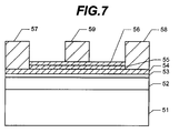
- Fig. 7 is a cross sectional view of the HEMT according to the second embodiment.
- an electron transport layer 52 made of non-doped GaN
- a non-doped layer 53 made of non-doped Al 0.25 Ga 0.75 N
- an electron supply layer 54 made of n-type Al 0.25 Ga 0.75 N.
- a source electrode 57 and a drain electrode 58 are disposed on the electron supply layer 54 at a distance from each other.
- a protective layer 55 of n-type GaN covers the surface of the electron supply layer 54 between the source electrode 57 and drain electrode 58.
- An insulating layer 56 of SiN is disposed on the protective layer 55.
- a gate electrode 59 is disposed in a partial surface area of the insulating layer 56. The gate electrode 59 is disposed at a distance from both the source electrode 57 and drain electrode 58.
- a thickness of the insulating layer 56 is set to 20 nm.
- the HEMT of the second embodiment has therefore not a Schottky gate structure but an insulated gate structure.
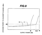
- Fig. 8 shows the relation between an output power of a Doherty amplifier and a leakage power to an adjacent channel.
- the abscissa represents an output power represented by a back-off amount from a saturation output in the unit of "dB”, and the ordinate represents a leakage power to an adjacent channel in the unit of "dBc”.
- a solid line b1 in Fig. 8 indicates the relation when the HEMT of the second embodiment is used in the carrier amplifier, and a solid line b0 indicates the relation when the HEMT of the Schottky gate structure without the insulating film 56 shown in Fig. 7 is used in the carrier amplifier.
- a gate length of the HEMT used for the carrier amplifier and peak amplifier is preferably set to a range between 0.3 ⁇ m and 0.7 ⁇ m, and more preferably to a range between 0.5 ⁇ m and 0.6 ⁇ m.
- the gate length is elongated, the gain of the Doherty amplifier decreases and distortion characteristics are deteriorated. If the gate length is shorter than 0.5 ⁇ m, the breakdown voltage is reduced to 200 V or lower. Efficiency is reduced because of deterioration of pinch-off characteristics, and reliability of the device worsens.
- a unit gate width is preferably set to a range between 200 ⁇ m and 350 ⁇ m, and more preferably to a range between 250 ⁇ m and 300 ⁇ m. As the unit gate width is widened, the gain of the Doherty amplifier goes down, whereas as the unit gate width is narrowed, a maximum power to be output is reduced.
- the upper electron supply layer 7 may be made of AlGalnN instead of AlGaN.
- the threshold voltage of the HEMT can be changed by controlling an atomic ratio In/(group III element) to adjust a band gap of the upper electron supply layer 4.
- Each of the electron transport layer, electron supply layer and the like may be made of other compound semiconductor materials.
Landscapes
- Engineering & Computer Science (AREA)
- Power Engineering (AREA)
- Junction Field-Effect Transistors (AREA)
- Thin Film Transistor (AREA)
- Insulated Gate Type Field-Effect Transistor (AREA)
- Amplifiers (AREA)
Applications Claiming Priority (1)
| Application Number | Priority Date | Filing Date | Title |
|---|---|---|---|
| JP2007048053A JP4967708B2 (ja) | 2007-02-27 | 2007-02-27 | 化合物半導体装置及びそれを用いたドハティ増幅器 |
Publications (3)
| Publication Number | Publication Date |
|---|---|
| EP1965434A2 true EP1965434A2 (fr) | 2008-09-03 |
| EP1965434A3 EP1965434A3 (fr) | 2009-04-15 |
| EP1965434B1 EP1965434B1 (fr) | 2015-08-19 |
Family
ID=39432208
Family Applications (1)
| Application Number | Title | Priority Date | Filing Date |
|---|---|---|---|
| EP08101728.7A Ceased EP1965434B1 (fr) | 2007-02-27 | 2008-02-19 | Dispositif de semi-conducteur à composant et amplificateur Doherty utilisant un dispositif de semi-conducteur à composant |
Country Status (4)
| Country | Link |
|---|---|
| US (2) | US7663162B2 (fr) |
| EP (1) | EP1965434B1 (fr) |
| JP (1) | JP4967708B2 (fr) |
| KR (1) | KR100967779B1 (fr) |
Cited By (1)
| Publication number | Priority date | Publication date | Assignee | Title |
|---|---|---|---|---|
| WO2021197703A1 (fr) * | 2020-03-30 | 2021-10-07 | Otto-Von-Guericke-Universität Magdeburg | Transistor à effet de champ |
Families Citing this family (20)
| Publication number | Priority date | Publication date | Assignee | Title |
|---|---|---|---|---|
| JP2010135640A (ja) * | 2008-12-05 | 2010-06-17 | Panasonic Corp | 電界効果トランジスタ |
| JP5544713B2 (ja) * | 2008-12-26 | 2014-07-09 | 富士通株式会社 | 化合物半導体装置及びその製造方法 |
| US20120032738A1 (en) * | 2009-04-28 | 2012-02-09 | Panasonic Corporation | Power amplifier |
| KR101219441B1 (ko) * | 2010-12-27 | 2013-01-11 | 전자부품연구원 | 미세 게이트 컨택홀을 갖는 질화물계 반도체 소자 및 그의 제조 방법 |
| KR20120120826A (ko) * | 2011-04-25 | 2012-11-02 | 삼성전기주식회사 | 질화물 반도체 소자 및 그 제조방법 |
| US8710511B2 (en) * | 2011-07-29 | 2014-04-29 | Northrop Grumman Systems Corporation | AIN buffer N-polar GaN HEMT profile |
| JP5987288B2 (ja) * | 2011-09-28 | 2016-09-07 | 富士通株式会社 | 半導体装置 |
| JP5790461B2 (ja) * | 2011-12-07 | 2015-10-07 | 富士通株式会社 | 化合物半導体装置及びその製造方法 |
| US9407214B2 (en) * | 2013-06-28 | 2016-08-02 | Cree, Inc. | MMIC power amplifier |
| KR101480068B1 (ko) * | 2013-10-18 | 2015-01-09 | 경북대학교 산학협력단 | 질화물 반도체 소자 및 그 제조방법 |
| JP6341679B2 (ja) * | 2014-02-06 | 2018-06-13 | ルネサスエレクトロニクス株式会社 | 半導体装置 |
| US20150364330A1 (en) | 2014-06-11 | 2015-12-17 | Hrl Laboratories Llc | Ta based au-free ohmic contacts in advanced aigan/gan based hfets and/or moshfets for power switch applications |
| JP6313509B2 (ja) * | 2017-07-18 | 2018-04-18 | 株式会社東芝 | 半導体装置 |
| US10741494B2 (en) | 2018-11-07 | 2020-08-11 | Semiconductor Components Industries, Llc | Electronic device including a contact structure contacting a layer |
| US12628368B2 (en) * | 2019-02-05 | 2026-05-12 | Mitsubishi Electric Corporation | Semiconductor device and method of manufacturing semiconductor device |
| JP7192099B2 (ja) * | 2019-04-01 | 2022-12-19 | ヌヴォトンテクノロジージャパン株式会社 | モノリシック半導体装置およびハイブリッド半導体装置 |
| US11887945B2 (en) * | 2020-09-30 | 2024-01-30 | Wolfspeed, Inc. | Semiconductor device with isolation and/or protection structures |
| WO2023178683A1 (fr) * | 2022-03-25 | 2023-09-28 | 华为技术有限公司 | Transistor à haute mobilité électronique, amplificateur de puissance de doherty et dispositif électronique |
| TWI826058B (zh) * | 2022-10-20 | 2023-12-11 | 國立陽明交通大學 | 高電子移動率電晶體 |
| WO2025197830A1 (fr) * | 2024-03-21 | 2025-09-25 | ヌヴォトンテクノロジージャパン株式会社 | Amplificateur doherty |
Citations (1)
| Publication number | Priority date | Publication date | Assignee | Title |
|---|---|---|---|---|
| WO2000065663A1 (fr) | 1999-04-26 | 2000-11-02 | Kansai Research Institute | Transistor a heterostructure a effet de champ |
Family Cites Families (8)
| Publication number | Priority date | Publication date | Assignee | Title |
|---|---|---|---|---|
| JP3233167B2 (ja) * | 1992-03-23 | 2001-11-26 | 住友電気工業株式会社 | 半導体装置 |
| CA2091926A1 (fr) | 1992-03-23 | 1993-09-24 | Shigeru Nakajima | Dispositif a semiconducteurs |
| JP2500457B2 (ja) * | 1993-06-17 | 1996-05-29 | 日本電気株式会社 | ヘテロ接合電界効果トランジスタ |
| JP2001308315A (ja) * | 2000-04-26 | 2001-11-02 | Hitachi Cable Ltd | Iii−v族化合物半導体エピタキシャルウェハ |
| JP4117535B2 (ja) * | 2001-11-30 | 2008-07-16 | 信越半導体株式会社 | 化合物半導体素子 |
| JP5216184B2 (ja) | 2004-12-07 | 2013-06-19 | 富士通株式会社 | 化合物半導体装置およびその製造方法 |
| JP2006166141A (ja) | 2004-12-08 | 2006-06-22 | Matsushita Electric Ind Co Ltd | ドハティ増幅器 |
| US7253454B2 (en) * | 2005-03-03 | 2007-08-07 | Cree, Inc. | High electron mobility transistor |
-
2007
- 2007-02-27 JP JP2007048053A patent/JP4967708B2/ja not_active Expired - Fee Related
-
2008
- 2008-02-19 EP EP08101728.7A patent/EP1965434B1/fr not_active Ceased
- 2008-02-19 US US12/071,219 patent/US7663162B2/en active Active
- 2008-02-26 KR KR1020080017016A patent/KR100967779B1/ko not_active Expired - Fee Related
-
2009
- 2009-11-24 US US12/591,574 patent/US7777251B2/en active Active
Patent Citations (1)
| Publication number | Priority date | Publication date | Assignee | Title |
|---|---|---|---|---|
| WO2000065663A1 (fr) | 1999-04-26 | 2000-11-02 | Kansai Research Institute | Transistor a heterostructure a effet de champ |
Non-Patent Citations (2)
| Title |
|---|
| CHEN K J ET AL.: "AIGaN-GaN Double-Channel HEMTs" IEEE TRANSACTIONS ON ELECTRON DEVICES", IEEE SERVICE CENTER, vol. 52, no. 4, 1 April 2005 (2005-04-01), pages 438 - 446 |
| KEVIN J WEBB ET AL.: "Fabrication and Operation of a Velocity Modulation Transistor", IEEE TRANSACTIONS ON ELECTRON DEVICES, vol. 48, no. 12, 1 December 2001 (2001-12-01) |
Cited By (1)
| Publication number | Priority date | Publication date | Assignee | Title |
|---|---|---|---|---|
| WO2021197703A1 (fr) * | 2020-03-30 | 2021-10-07 | Otto-Von-Guericke-Universität Magdeburg | Transistor à effet de champ |
Also Published As
| Publication number | Publication date |
|---|---|
| EP1965434A3 (fr) | 2009-04-15 |
| EP1965434B1 (fr) | 2015-08-19 |
| KR100967779B1 (ko) | 2010-07-05 |
| KR20080079604A (ko) | 2008-09-01 |
| US20080204140A1 (en) | 2008-08-28 |
| JP4967708B2 (ja) | 2012-07-04 |
| JP2008211089A (ja) | 2008-09-11 |
| US7663162B2 (en) | 2010-02-16 |
| US20100066451A1 (en) | 2010-03-18 |
| US7777251B2 (en) | 2010-08-17 |
Similar Documents
| Publication | Publication Date | Title |
|---|---|---|
| EP1965434B1 (fr) | Dispositif de semi-conducteur à composant et amplificateur Doherty utilisant un dispositif de semi-conducteur à composant | |
| US7687828B2 (en) | Field-effect transistor | |
| JP4469139B2 (ja) | 化合物半導体fet | |
| JP6151487B2 (ja) | 化合物半導体装置及びその製造方法 | |
| JP3393602B2 (ja) | 半導体装置 | |
| JP4592938B2 (ja) | 半導体装置 | |
| JP4117535B2 (ja) | 化合物半導体素子 | |
| JP5825017B2 (ja) | 化合物半導体装置及びその製造方法 | |
| US7985984B2 (en) | III-nitride semiconductor field effect transistor | |
| KR20100015747A (ko) | 공핍형 GaN 기반 FET를 이용하는 캐스코드 회로 | |
| WO2010064362A1 (fr) | Transistor à effet de champ | |
| CN103715242A (zh) | 半导体装置 | |
| CN106057648A (zh) | 化合物半导体器件及其制造方法 | |
| US10600901B2 (en) | Compound semiconductor device and manufacturing method thereof | |
| US10847642B2 (en) | Compound semiconductor device and fabrication method | |
| US11024730B2 (en) | Nitride semiconductor device and manufacturing method for the same | |
| US9691890B2 (en) | Compound semiconductor device and manufacturing method thereof | |
| JP6233476B2 (ja) | 化合物半導体装置 | |
| JP2010040828A (ja) | 窒化物半導体装置 | |
| JP2012049170A (ja) | 窒化物半導体装置 | |
| JP5509544B2 (ja) | 半導体装置及びその製造方法 | |
| WO2011046213A1 (fr) | Dispositif à semi-conducteur au nitrure et dispositif électronique | |
| JP2024062415A (ja) | 窒化ガリウムベースの高電子移動度トランジスタの改良型バックバリア | |
| CN118039665A (zh) | 一种半导体器件的外延结构及其制备方法、半导体器件 | |
| CN121420651A (zh) | Iii-n双栅器件 |
Legal Events
| Date | Code | Title | Description |
|---|---|---|---|
| PUAI | Public reference made under article 153(3) epc to a published international application that has entered the european phase |
Free format text: ORIGINAL CODE: 0009012 |
|
| AK | Designated contracting states |
Kind code of ref document: A2 Designated state(s): AT BE BG CH CY CZ DE DK EE ES FI FR GB GR HR HU IE IS IT LI LT LU LV MC MT NL NO PL PT RO SE SI SK TR |
|
| AX | Request for extension of the european patent |
Extension state: AL BA MK RS |
|
| PUAL | Search report despatched |
Free format text: ORIGINAL CODE: 0009013 |
|
| AK | Designated contracting states |
Kind code of ref document: A3 Designated state(s): AT BE BG CH CY CZ DE DK EE ES FI FR GB GR HR HU IE IS IT LI LT LU LV MC MT NL NO PL PT RO SE SI SK TR |
|
| AX | Request for extension of the european patent |
Extension state: AL BA MK RS |
|
| 17P | Request for examination filed |
Effective date: 20091012 |
|
| AKX | Designation fees paid |
Designated state(s): DE GB |
|
| 17Q | First examination report despatched |
Effective date: 20120302 |
|
| GRAP | Despatch of communication of intention to grant a patent |
Free format text: ORIGINAL CODE: EPIDOSNIGR1 |
|
| INTG | Intention to grant announced |
Effective date: 20150407 |
|
| RIC1 | Information provided on ipc code assigned before grant |
Ipc: H03F 1/02 20060101ALI20150323BHEP Ipc: H01L 29/20 20060101ALN20150323BHEP Ipc: H01L 21/338 20060101ALI20150323BHEP Ipc: H01L 29/45 20060101ALN20150323BHEP Ipc: H01L 29/778 20060101AFI20150323BHEP |
|
| GRAS | Grant fee paid |
Free format text: ORIGINAL CODE: EPIDOSNIGR3 |
|
| GRAA | (expected) grant |
Free format text: ORIGINAL CODE: 0009210 |
|
| AK | Designated contracting states |
Kind code of ref document: B1 Designated state(s): DE GB |
|
| REG | Reference to a national code |
Ref country code: GB Ref legal event code: FG4D |
|
| REG | Reference to a national code |
Ref country code: DE Ref legal event code: R096 Ref document number: 602008039629 Country of ref document: DE |
|
| REG | Reference to a national code |
Ref country code: DE Ref legal event code: R097 Ref document number: 602008039629 Country of ref document: DE |
|
| PLBE | No opposition filed within time limit |
Free format text: ORIGINAL CODE: 0009261 |
|
| STAA | Information on the status of an ep patent application or granted ep patent |
Free format text: STATUS: NO OPPOSITION FILED WITHIN TIME LIMIT |
|
| 26N | No opposition filed |
Effective date: 20160520 |
|
| PGFP | Annual fee paid to national office [announced via postgrant information from national office to epo] |
Ref country code: GB Payment date: 20211230 Year of fee payment: 15 |
|
| PGFP | Annual fee paid to national office [announced via postgrant information from national office to epo] |
Ref country code: DE Payment date: 20211230 Year of fee payment: 15 |
|
| REG | Reference to a national code |
Ref country code: DE Ref legal event code: R119 Ref document number: 602008039629 Country of ref document: DE |
|
| GBPC | Gb: european patent ceased through non-payment of renewal fee |
Effective date: 20230219 |
|
| PG25 | Lapsed in a contracting state [announced via postgrant information from national office to epo] |
Ref country code: GB Free format text: LAPSE BECAUSE OF NON-PAYMENT OF DUE FEES Effective date: 20230219 |
|
| PG25 | Lapsed in a contracting state [announced via postgrant information from national office to epo] |
Ref country code: GB Free format text: LAPSE BECAUSE OF NON-PAYMENT OF DUE FEES Effective date: 20230219 Ref country code: DE Free format text: LAPSE BECAUSE OF NON-PAYMENT OF DUE FEES Effective date: 20230901 |