EP1965619A2 - Connexion de compression pour paquets de CI verticaux - Google Patents
Connexion de compression pour paquets de CI verticaux Download PDFInfo
- Publication number
- EP1965619A2 EP1965619A2 EP08151443A EP08151443A EP1965619A2 EP 1965619 A2 EP1965619 A2 EP 1965619A2 EP 08151443 A EP08151443 A EP 08151443A EP 08151443 A EP08151443 A EP 08151443A EP 1965619 A2 EP1965619 A2 EP 1965619A2
- Authority
- EP
- European Patent Office
- Prior art keywords
- package
- circuit device
- integrated circuit
- electrical contact
- electrically conductive
- Prior art date
- Legal status (The legal status is an assumption and is not a legal conclusion. Google has not performed a legal analysis and makes no representation as to the accuracy of the status listed.)
- Withdrawn
Links
Images
Classifications
-
- H—ELECTRICITY
- H05—ELECTRIC TECHNIQUES NOT OTHERWISE PROVIDED FOR
- H05K—PRINTED CIRCUITS; CASINGS OR CONSTRUCTIONAL DETAILS OF ELECTRIC APPARATUS; MANUFACTURE OF ASSEMBLAGES OF ELECTRICAL COMPONENTS
- H05K7/00—Constructional details common to different types of electric apparatus
- H05K7/20—Modifications to facilitate cooling, ventilating, or heating
- H05K7/2039—Modifications to facilitate cooling, ventilating, or heating characterised by the heat transfer by conduction from the heat generating element to a dissipating body
- H05K7/20436—Inner thermal coupling elements in heat dissipating housings, e.g. protrusions or depressions integrally formed in the housing
- H05K7/2049—Pressing means used to urge contact, e.g. springs
-
- H—ELECTRICITY
- H10—SEMICONDUCTOR DEVICES; ELECTRIC SOLID-STATE DEVICES NOT OTHERWISE PROVIDED FOR
- H10W—GENERIC PACKAGES, INTERCONNECTIONS, CONNECTORS OR OTHER CONSTRUCTIONAL DETAILS OF DEVICES COVERED BY CLASS H10
- H10W72/00—Interconnections or connectors in packages
-
- H—ELECTRICITY
- H10—SEMICONDUCTOR DEVICES; ELECTRIC SOLID-STATE DEVICES NOT OTHERWISE PROVIDED FOR
- H10W—GENERIC PACKAGES, INTERCONNECTIONS, CONNECTORS OR OTHER CONSTRUCTIONAL DETAILS OF DEVICES COVERED BY CLASS H10
- H10W90/00—Package configurations
-
- H—ELECTRICITY
- H10—SEMICONDUCTOR DEVICES; ELECTRIC SOLID-STATE DEVICES NOT OTHERWISE PROVIDED FOR
- H10W—GENERIC PACKAGES, INTERCONNECTIONS, CONNECTORS OR OTHER CONSTRUCTIONAL DETAILS OF DEVICES COVERED BY CLASS H10
- H10W72/00—Interconnections or connectors in packages
- H10W72/90—Bond pads, in general
- H10W72/941—Dispositions of bond pads
- H10W72/944—Dispositions of multiple bond pads
-
- H—ELECTRICITY
- H10—SEMICONDUCTOR DEVICES; ELECTRIC SOLID-STATE DEVICES NOT OTHERWISE PROVIDED FOR
- H10W—GENERIC PACKAGES, INTERCONNECTIONS, CONNECTORS OR OTHER CONSTRUCTIONAL DETAILS OF DEVICES COVERED BY CLASS H10
- H10W72/00—Interconnections or connectors in packages
- H10W72/90—Bond pads, in general
- H10W72/951—Materials of bond pads
- H10W72/952—Materials of bond pads comprising metals or metalloids, e.g. PbSn, Ag or Cu
-
- H—ELECTRICITY
- H10—SEMICONDUCTOR DEVICES; ELECTRIC SOLID-STATE DEVICES NOT OTHERWISE PROVIDED FOR
- H10W—GENERIC PACKAGES, INTERCONNECTIONS, CONNECTORS OR OTHER CONSTRUCTIONAL DETAILS OF DEVICES COVERED BY CLASS H10
- H10W74/00—Encapsulations, e.g. protective coatings
Definitions
- the invention relates to integrated circuits (IC) packages, and more particularly to electrical connections for high current vertical device IC packages.
- circuit board components have been specifically developed for high current and high power applications, such as hybrid and electric vehicles.
- Such components often comprise a semiconductor device, such as a diode, thyristor, metal oxide semiconductor field effect transistor (MOSFET), isolated gate bipolar transistor (IGBT), resistors, etc., depending on the particular circuit and use desired.
- MOSFET metal oxide semiconductor field effect transistor
- IGBT isolated gate bipolar transistor
- resistors etc., depending on the particular circuit and use desired.
- Vertical devices are typically formed in a semiconductor (e.g., silicon) die having metalized electrodes on its opposite surfaces, e.g., a MOSFET or IGBT with a drain/collector electrode on one surface and gate and source/emitter electrodes on its opposite surface.
- the die is mounted on a conductive pad for electrical contact with the drain/collector electrode, with connections to the remaining electrodes on the opposite surface often being made by wire bonding.
- the pad and wires are electrically connected to a lead frame having leads projecting outside a protective housing that is often formed by overmolding the lead frame and die.
- Components of the type described above include well-known industry standard packages, such as the TO 220 and TO 247 packages, which are prepackaged integrated circuit components having leads adapted for attachment (e.g., by soldering) to a printed circuit board (PCB).
- the overmolded housings of these packages protect the die, wire bonds, etc., while typically leaving the lower surfaces of the conductive pad exposed to provide a thermal and/or electrical path out of the package. Such a path allows the package to be connected to an electrical bus for electric connection to the PCB, or a heat-sinking mass for dissipation of heat from the package.
- the conventional high power and high current vertical device IC packaging concepts have electrical connection methods that utilize either a wire bond approach or a complicated package with dual solder joints. These solder joints have a reduced life due to high stresses created from the mismatch between the coefficient of thermal expansion of the substrate and the coefficient of thermal expansion of the rather large integrated circuit. This mismatch becomes an even greater problem with the use of a copper slug to mount the IC device. Accordingly, improved connection technology that does not use a wire bond approach or solder joints is desired.
- the invention involves the use of a compression electrical connection for vertical IC devices.
- springs e.g., elastomers or metal leaf or coil springs
- under compression provide a clamping force to ensure electrical contact of an integrated circuit device to a printed circuit board.
- thermoset overmold process is used to provide a force to form the compression electrical connections.
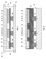
- FIG. 1 Shown in FIG. 1 is a vertical device integrated circuit package 10 utilizing springs 12a, 12b and 12c that are under compression to provide a claming force to ensure electrical contact of an integrated circuit device 14 (e.g., an IGBT) with a printed circuit board 16.
- Integrated circuit device 14 is a vertical device, more particularly, an IGBT, having metalized electrodes (electrical contacts) 20, 21 on opposite surfaces.
- An electrically conductive element 24 e.g., copper strap
- electrical contact 20 of IGBT with an electrical contact 26 on printed circuit board 16 while the electrical contact 21 on the opposite side of IGBT 14 is electrically connected to a separate electrical contact 28 on printed circuit board 16.
- a diode 32 is included in package 10.
- Diode 32 includes an electrical contact 30 electrically connected to conductive element 24 and a second electrical contact 34 on a surface opposite the surface on which electrical contact 30 is located, which is electrically connected to a contact pad 36 on printed circuit board 16.
- the entire assembly, including elastomeric springs 12a, 12b and 12c is sandwiched between a heat sink 40 and a cover member 42.
- Fasteners 44 e.g., screws
- sufficient compression is applied to compress resiliently deformable spring members 12a, 12b, and 12c so that they urge electrical contacts together to establish compression electrical connections between corresponding electrical contacts.
- the springs are preferably located directly under the interfacing electrical contacts. That is, the compressive forces from springs 12a, 12b and 12c have a vector orthogonal to and passing through the interfacing contacts of the compression electrical connections.
- the contacts 20, 21, 30, 34, 28, 36 and 46 are gold-plated.
- gold-plating be provided on electrically conductive element 24 as indicated by reference numerals 26, 47 and 48.
- a thermal interface material 50 may be disposed between electrically conductive element 24 and heat sink 40 to enhance heat transfer through conductive element 24 and into heat sink 40, where heat can be efficiently transferred to the surrounding atmosphere.
- the thermal interface material may also provide dielectric isolation.
- Springs 12a, 12b and 12c may comprise an elastomeric material, or a metal spring (e.g., a coil spring or leaf spring).
- compression spring members can be formed in situ during an overmolding process. This can be achieved using spring pressure pins 60 (which are part of molding tool 62) to temporarily hold the assembly together during an overmolding process.
- Springs 60 provide a specific force so that the molding composition (e.g., a thermoset epoxy resin) does not flow into gaps between the integrated circuit and the printed circuit board or between the integrated circuit board and the electrically conductive element.
- the molding composition e.g., a thermoset epoxy resin
- pins 60 are retracted and the molding composition fills the volume vacated by retraction of pins 60.
- the pins may provide forces during the entire molding process, and be retracted when the mold cavity is opened.
- the holes formed by the pins can then be filled with epoxy after the molding process.
- the molding composition adhesively bonds the printed circuit board, heat sink, and electrically conductive strip together.
- the maximum use temperature is always below the zero-stress state (165°C. molding temperature). This coupled with use of a material having a low coefficient of thermal expansion keeps the structure in compression. Mold locking features can also be employed in the heat sink, printed circuit board and other components of the package to mechanically lock the structure together.
- Advantages of the invention include simplified manufacturing, high current connection formed by gold-to-gold contact surfaces, no solder cracking to silicon integrated circuit connections, repairability (for FIG. 1 design only), and the absence of leads (i.e., solder-free package).
Landscapes
- Physics & Mathematics (AREA)
- Thermal Sciences (AREA)
- Engineering & Computer Science (AREA)
- Microelectronics & Electronic Packaging (AREA)
- Cooling Or The Like Of Semiconductors Or Solid State Devices (AREA)
- Structures For Mounting Electric Components On Printed Circuit Boards (AREA)
Applications Claiming Priority (1)
| Application Number | Priority Date | Filing Date | Title |
|---|---|---|---|
| US11/712,718 US7447041B2 (en) | 2007-03-01 | 2007-03-01 | Compression connection for vertical IC packages |
Publications (2)
| Publication Number | Publication Date |
|---|---|
| EP1965619A2 true EP1965619A2 (fr) | 2008-09-03 |
| EP1965619A3 EP1965619A3 (fr) | 2009-12-23 |
Family
ID=39529144
Family Applications (1)
| Application Number | Title | Priority Date | Filing Date |
|---|---|---|---|
| EP08151443A Withdrawn EP1965619A3 (fr) | 2007-03-01 | 2008-02-14 | Connexion de compression pour paquets de CI verticaux |
Country Status (2)
| Country | Link |
|---|---|
| US (1) | US7447041B2 (fr) |
| EP (1) | EP1965619A3 (fr) |
Cited By (2)
| Publication number | Priority date | Publication date | Assignee | Title |
|---|---|---|---|---|
| CN104517954A (zh) * | 2013-10-02 | 2015-04-15 | 英飞凌科技奥地利有限公司 | 在两个衬底之间具有半导体芯片的晶体管布置 |
| US9526191B2 (en) | 2013-05-15 | 2016-12-20 | Dy 4 Systems Inc. | Fluid cooled enclosure for circuit module apparatus and methods of cooling a conduction cooled circuit module |
Families Citing this family (3)
| Publication number | Priority date | Publication date | Assignee | Title |
|---|---|---|---|---|
| US9093766B2 (en) * | 2013-09-25 | 2015-07-28 | Ford Global Technologies, Llc | Conductive ink elastomeric molded connector |
| US11217505B2 (en) | 2019-09-10 | 2022-01-04 | Aptiv Technologies Limited | Heat exchanger for electronics |
| US12471221B2 (en) | 2022-10-21 | 2025-11-11 | Raytheon Company | Clamping device with pivoting retainer |
Citations (1)
| Publication number | Priority date | Publication date | Assignee | Title |
|---|---|---|---|---|
| DE102004018477A1 (de) | 2004-04-16 | 2005-11-03 | eupec Europäische Gesellschaft für Leistungshalbleiter mbH | Halbleitermodul |
Family Cites Families (27)
| Publication number | Priority date | Publication date | Assignee | Title |
|---|---|---|---|---|
| US4607276A (en) * | 1984-03-08 | 1986-08-19 | Olin Corporation | Tape packages |
| US5345107A (en) * | 1989-09-25 | 1994-09-06 | Hitachi, Ltd. | Cooling apparatus for electronic device |
| JP2755761B2 (ja) * | 1990-01-26 | 1998-05-25 | 株式会社東芝 | 半導体装置 |
| JP3137375B2 (ja) * | 1990-09-20 | 2001-02-19 | 株式会社東芝 | 圧接型半導体装置 |
| US5210939A (en) * | 1992-04-17 | 1993-05-18 | Intel Corporation | Lead grid array integrated circuit |
| US6456100B1 (en) * | 1998-01-20 | 2002-09-24 | Micron Technology, Inc. | Apparatus for attaching to a semiconductor |
| US6476481B2 (en) * | 1998-05-05 | 2002-11-05 | International Rectifier Corporation | High current capacity semiconductor device package and lead frame with large area connection posts and modified outline |
| JP2001036002A (ja) * | 1999-07-23 | 2001-02-09 | Fuji Electric Co Ltd | 半導体装置 |
| US6703707B1 (en) * | 1999-11-24 | 2004-03-09 | Denso Corporation | Semiconductor device having radiation structure |
| JP3510838B2 (ja) * | 2000-03-24 | 2004-03-29 | 三洋電機株式会社 | 半導体装置およびその製造方法 |
| US6624522B2 (en) * | 2000-04-04 | 2003-09-23 | International Rectifier Corporation | Chip scale surface mounted device and process of manufacture |
| JP2002151550A (ja) * | 2000-11-15 | 2002-05-24 | Nec Corp | 半導体装置、その製造方法並びに製造に使用するコイルスプリング切断治具及びコイルスプリング供給治具 |
| US6784540B2 (en) * | 2001-10-10 | 2004-08-31 | International Rectifier Corp. | Semiconductor device package with improved cooling |
| US6545879B1 (en) * | 2002-01-10 | 2003-04-08 | Tyco Electronics Corporation | Method and apparatus for mounting a lidless semiconductor device |
| US20040094828A1 (en) * | 2002-01-16 | 2004-05-20 | Delphi Technologies, Inc. | Double-sided multi-chip circuit component |
| KR100791136B1 (ko) * | 2002-04-16 | 2008-01-02 | 닛폰 하츠죠 가부시키가이샤 | 도전성 접촉자용 홀더 |
| US7029288B2 (en) * | 2003-03-24 | 2006-04-18 | Che-Yu Li | Electrical contact and connector and method of manufacture |
| US7042080B2 (en) * | 2003-07-14 | 2006-05-09 | Micron Technology, Inc. | Semiconductor interconnect having compliant conductive contacts |
| US20060151868A1 (en) * | 2005-01-10 | 2006-07-13 | Zhu Tinggang | Package for gallium nitride semiconductor devices |
| US7229855B2 (en) * | 2005-02-23 | 2007-06-12 | Delphi Technologies, Inc. | Process for assembling a double-sided circuit component |
| US7443014B2 (en) * | 2005-10-25 | 2008-10-28 | Infineon Technologies Ag | Electronic module and method of assembling the same |
| US7678609B2 (en) * | 2005-11-03 | 2010-03-16 | International Rectifier Corporation | Semiconductor package with redistributed pads |
| WO2007058854A2 (fr) * | 2005-11-10 | 2007-05-24 | International Rectifier Corporation | Boitier de semi-conducteur comprenant une microplaquette semi-conductrice a plots conducteurs redistribues |
| US7291869B2 (en) * | 2006-02-06 | 2007-11-06 | Infieon Technologies A.G. | Electronic module with stacked semiconductors |
| US8354692B2 (en) * | 2006-03-15 | 2013-01-15 | Infineon Technologies Ag | Vertical semiconductor power switch, electronic component and methods of producing the same |
| US7598603B2 (en) * | 2006-03-15 | 2009-10-06 | Infineon Technologies Ag | Electronic component having a power switch with an anode thereof mounted on a die attach region of a heat sink |
| EP1860696A1 (fr) * | 2006-05-26 | 2007-11-28 | Abb Research Ltd. | Module à semi-comducteur |
-
2007
- 2007-03-01 US US11/712,718 patent/US7447041B2/en not_active Expired - Fee Related
-
2008
- 2008-02-14 EP EP08151443A patent/EP1965619A3/fr not_active Withdrawn
Patent Citations (1)
| Publication number | Priority date | Publication date | Assignee | Title |
|---|---|---|---|---|
| DE102004018477A1 (de) | 2004-04-16 | 2005-11-03 | eupec Europäische Gesellschaft für Leistungshalbleiter mbH | Halbleitermodul |
Cited By (5)
| Publication number | Priority date | Publication date | Assignee | Title |
|---|---|---|---|---|
| US9526191B2 (en) | 2013-05-15 | 2016-12-20 | Dy 4 Systems Inc. | Fluid cooled enclosure for circuit module apparatus and methods of cooling a conduction cooled circuit module |
| EP2804456B1 (fr) * | 2013-05-15 | 2019-07-31 | DY 4 Systems Inc. | Enceinte refroidie par un fluide pour module de circuit |
| CN104517954A (zh) * | 2013-10-02 | 2015-04-15 | 英飞凌科技奥地利有限公司 | 在两个衬底之间具有半导体芯片的晶体管布置 |
| CN104517954B (zh) * | 2013-10-02 | 2017-10-03 | 英飞凌科技奥地利有限公司 | 在两个衬底之间具有半导体芯片的晶体管布置 |
| US9806029B2 (en) | 2013-10-02 | 2017-10-31 | Infineon Technologies Austria Ag | Transistor arrangement with semiconductor chips between two substrates |
Also Published As
| Publication number | Publication date |
|---|---|
| US20080212296A1 (en) | 2008-09-04 |
| EP1965619A3 (fr) | 2009-12-23 |
| US7447041B2 (en) | 2008-11-04 |
Similar Documents
| Publication | Publication Date | Title |
|---|---|---|
| KR102585450B1 (ko) | 브레이징된 전기 전도성 층을 포함하는 칩 캐리어를 구비한 몰딩된 패키지 | |
| US9209114B2 (en) | Power module package with a fastening unit including a non-conductive portion | |
| CN107170718B (zh) | 半导体模块 | |
| US8451621B2 (en) | Semiconductor component and method of manufacture | |
| US20230215788A1 (en) | Power module and manufacturing method thereof, converter, and electronic device | |
| US12041755B2 (en) | Power semiconductor module arrangement and method for producing a power semiconductor module arrangement | |
| US20080191340A1 (en) | Power Semiconductor Module And Method For Its Manufacture | |
| TWI647995B (zh) | 插拔式功率模組及次系統 | |
| US12494418B2 (en) | Power module with press-fit contacts | |
| CN103779295A (zh) | 功率模块封装 | |
| US20230026022A1 (en) | Power Module with Press-Fit Contacts | |
| US7447041B2 (en) | Compression connection for vertical IC packages | |
| CN114446916A (zh) | 三层级互连夹 | |
| US12476397B2 (en) | Transfer molded power modules and methods of manufacture | |
| US9099451B2 (en) | Power module package and method of manufacturing the same | |
| EP2058860A2 (fr) | Ensemble de moule à montage en surface entièrement testable configuré pour un refroidissement à double face | |
| EP1696484A1 (fr) | Procédé d'assemblage d'un composant de circuit à double face | |
| US20250140625A1 (en) | Semiconductor module and method of manufacturing a semiconductor module | |
| EP1531494A2 (fr) | Composant de circuit multipuce et double face | |
| CN116666312A (zh) | 陶瓷半导体器件封装件 | |
| US7453146B2 (en) | High power MCM package with improved planarity and heat dissipation | |
| US20230027138A1 (en) | Power module | |
| KR20260007176A (ko) | 성형 공동을 갖는 전력 반도체 패키지 | |
| KR20150049975A (ko) | 반도체 패키지 및 그 제조 방법 | |
| CN119816946A (zh) | 半导体装置 |
Legal Events
| Date | Code | Title | Description |
|---|---|---|---|
| PUAI | Public reference made under article 153(3) epc to a published international application that has entered the european phase |
Free format text: ORIGINAL CODE: 0009012 |
|
| AK | Designated contracting states |
Kind code of ref document: A2 Designated state(s): AT BE BG CH CY CZ DE DK EE ES FI FR GB GR HR HU IE IS IT LI LT LU LV MC MT NL NO PL PT RO SE SI SK TR |
|
| AX | Request for extension of the european patent |
Extension state: AL BA MK RS |
|
| PUAL | Search report despatched |
Free format text: ORIGINAL CODE: 0009013 |
|
| AK | Designated contracting states |
Kind code of ref document: A3 Designated state(s): AT BE BG CH CY CZ DE DK EE ES FI FR GB GR HR HU IE IS IT LI LT LU LV MC MT NL NO PL PT RO SE SI SK TR |
|
| AX | Request for extension of the european patent |
Extension state: AL BA MK RS |
|
| RIC1 | Information provided on ipc code assigned before grant |
Ipc: H05K 7/10 20060101ALI20080627BHEP Ipc: H01L 23/40 20060101ALI20080627BHEP Ipc: H05K 7/20 20060101AFI20091118BHEP |
|
| 17P | Request for examination filed |
Effective date: 20100623 |
|
| 17Q | First examination report despatched |
Effective date: 20100723 |
|
| AKX | Designation fees paid |
Designated state(s): AT BE BG CH CY CZ DE DK EE ES FI FR GB GR HR HU IE IS IT LI LT LU LV MC MT NL NO PL PT RO SE SI SK TR |
|
| GRAP | Despatch of communication of intention to grant a patent |
Free format text: ORIGINAL CODE: EPIDOSNIGR1 |
|
| GRAC | Information related to communication of intention to grant a patent modified |
Free format text: ORIGINAL CODE: EPIDOSCIGR1 |
|
| GRAJ | Information related to disapproval of communication of intention to grant by the applicant or resumption of examination proceedings by the epo deleted |
Free format text: ORIGINAL CODE: EPIDOSDIGR1 |
|
| RIC1 | Information provided on ipc code assigned before grant |
Ipc: H05K 7/20 20060101AFI20110913BHEP |
|
| STAA | Information on the status of an ep patent application or granted ep patent |
Free format text: STATUS: THE APPLICATION IS DEEMED TO BE WITHDRAWN |
|
| 18D | Application deemed to be withdrawn |
Effective date: 20110901 |