EP1967488A2 - Méthode de production de dispositif semi-conducteur et dispositif semi-conducteur, plus particulièrement capteur à membrane - Google Patents
Méthode de production de dispositif semi-conducteur et dispositif semi-conducteur, plus particulièrement capteur à membrane Download PDFInfo
- Publication number
- EP1967488A2 EP1967488A2 EP08104525A EP08104525A EP1967488A2 EP 1967488 A2 EP1967488 A2 EP 1967488A2 EP 08104525 A EP08104525 A EP 08104525A EP 08104525 A EP08104525 A EP 08104525A EP 1967488 A2 EP1967488 A2 EP 1967488A2
- Authority
- EP
- European Patent Office
- Prior art keywords
- region
- membrane
- semiconductor
- layer
- webs
- Prior art date
- Legal status (The legal status is an assumption and is not a legal conclusion. Google has not performed a legal analysis and makes no representation as to the accuracy of the status listed.)
- Withdrawn
Links
- 239000004065 semiconductor Substances 0.000 title claims abstract description 129
- 239000012528 membrane Substances 0.000 title claims abstract description 99
- 238000004519 manufacturing process Methods 0.000 title claims description 40
- 239000000463 material Substances 0.000 claims abstract description 59
- 238000000034 method Methods 0.000 claims description 67
- 239000000758 substrate Substances 0.000 claims description 62
- 230000008569 process Effects 0.000 claims description 42
- 229910052710 silicon Inorganic materials 0.000 claims description 38
- 239000010703 silicon Substances 0.000 claims description 38
- 238000000407 epitaxy Methods 0.000 claims description 24
- 238000000137 annealing Methods 0.000 claims description 20
- 238000005530 etching Methods 0.000 claims description 19
- 238000002048 anodisation reaction Methods 0.000 claims description 16
- 238000000151 deposition Methods 0.000 claims description 15
- 230000008021 deposition Effects 0.000 claims description 14
- 238000009432 framing Methods 0.000 claims description 13
- 238000004090 dissolution Methods 0.000 claims description 9
- 230000015572 biosynthetic process Effects 0.000 claims description 7
- 230000003647 oxidation Effects 0.000 claims description 7
- 238000007254 oxidation reaction Methods 0.000 claims description 7
- 230000008707 rearrangement Effects 0.000 claims description 6
- 238000000059 patterning Methods 0.000 claims description 4
- 239000000126 substance Substances 0.000 claims description 4
- 230000005855 radiation Effects 0.000 claims description 3
- 238000002161 passivation Methods 0.000 claims description 2
- 238000002360 preparation method Methods 0.000 claims description 2
- WGTYBPLFGIVFAS-UHFFFAOYSA-M tetramethylammonium hydroxide Chemical compound [OH-].C[N+](C)(C)C WGTYBPLFGIVFAS-UHFFFAOYSA-M 0.000 claims 2
- 238000007789 sealing Methods 0.000 claims 1
- 230000001427 coherent effect Effects 0.000 abstract description 3
- XUIMIQQOPSSXEZ-UHFFFAOYSA-N Silicon Chemical compound [Si] XUIMIQQOPSSXEZ-UHFFFAOYSA-N 0.000 description 38
- 238000002513 implantation Methods 0.000 description 22
- 239000011148 porous material Substances 0.000 description 16
- 229910021426 porous silicon Inorganic materials 0.000 description 12
- KRHYYFGTRYWZRS-UHFFFAOYSA-N hydrofluoric acid Substances F KRHYYFGTRYWZRS-UHFFFAOYSA-N 0.000 description 11
- 230000008901 benefit Effects 0.000 description 6
- 239000013078 crystal Substances 0.000 description 6
- 230000007547 defect Effects 0.000 description 6
- 230000000694 effects Effects 0.000 description 6
- 238000005286 illumination Methods 0.000 description 6
- 238000011161 development Methods 0.000 description 5
- QPJSUIGXIBEQAC-UHFFFAOYSA-N n-(2,4-dichloro-5-propan-2-yloxyphenyl)acetamide Chemical compound CC(C)OC1=CC(NC(C)=O)=C(Cl)C=C1Cl QPJSUIGXIBEQAC-UHFFFAOYSA-N 0.000 description 5
- 150000004767 nitrides Chemical class 0.000 description 5
- 229910004298 SiO 2 Inorganic materials 0.000 description 4
- 229910021421 monocrystalline silicon Inorganic materials 0.000 description 4
- 238000005496 tempering Methods 0.000 description 4
- 230000001133 acceleration Effects 0.000 description 3
- 229910021417 amorphous silicon Inorganic materials 0.000 description 3
- 238000009792 diffusion process Methods 0.000 description 3
- 230000035515 penetration Effects 0.000 description 3
- 230000000087 stabilizing effect Effects 0.000 description 3
- 230000007704 transition Effects 0.000 description 3
- 235000012431 wafers Nutrition 0.000 description 3
- NBIIXXVUZAFLBC-UHFFFAOYSA-N Phosphoric acid Chemical compound OP(O)(O)=O NBIIXXVUZAFLBC-UHFFFAOYSA-N 0.000 description 2
- ATUOYWHBWRKTHZ-UHFFFAOYSA-N Propane Chemical compound CCC ATUOYWHBWRKTHZ-UHFFFAOYSA-N 0.000 description 2
- 229910052581 Si3N4 Inorganic materials 0.000 description 2
- 230000006978 adaptation Effects 0.000 description 2
- 210000003323 beak Anatomy 0.000 description 2
- 239000000969 carrier Substances 0.000 description 2
- 238000010438 heat treatment Methods 0.000 description 2
- 230000000873 masking effect Effects 0.000 description 2
- 229920002120 photoresistant polymer Polymers 0.000 description 2
- 230000009467 reduction Effects 0.000 description 2
- HQVNEWCFYHHQES-UHFFFAOYSA-N silicon nitride Chemical compound N12[Si]34N5[Si]62N3[Si]51N64 HQVNEWCFYHHQES-UHFFFAOYSA-N 0.000 description 2
- UFHFLCQGNIYNRP-UHFFFAOYSA-N Hydrogen Chemical compound [H][H] UFHFLCQGNIYNRP-UHFFFAOYSA-N 0.000 description 1
- 208000012868 Overgrowth Diseases 0.000 description 1
- BLRPTPMANUNPDV-UHFFFAOYSA-N Silane Chemical compound [SiH4] BLRPTPMANUNPDV-UHFFFAOYSA-N 0.000 description 1
- VYPSYNLAJGMNEJ-UHFFFAOYSA-N Silicium dioxide Chemical compound O=[Si]=O VYPSYNLAJGMNEJ-UHFFFAOYSA-N 0.000 description 1
- 230000002411 adverse Effects 0.000 description 1
- 229910000147 aluminium phosphate Inorganic materials 0.000 description 1
- 238000005280 amorphization Methods 0.000 description 1
- XKRFYHLGVUSROY-UHFFFAOYSA-N argon Substances [Ar] XKRFYHLGVUSROY-UHFFFAOYSA-N 0.000 description 1
- 229910052786 argon Inorganic materials 0.000 description 1
- -1 argon ions Chemical class 0.000 description 1
- QVGXLLKOCUKJST-UHFFFAOYSA-N atomic oxygen Chemical compound [O] QVGXLLKOCUKJST-UHFFFAOYSA-N 0.000 description 1
- 239000002800 charge carrier Substances 0.000 description 1
- 239000011248 coating agent Substances 0.000 description 1
- 238000000576 coating method Methods 0.000 description 1
- 230000002950 deficient Effects 0.000 description 1
- 230000001419 dependent effect Effects 0.000 description 1
- 230000001627 detrimental effect Effects 0.000 description 1
- 239000002019 doping agent Substances 0.000 description 1
- 238000001312 dry etching Methods 0.000 description 1
- 230000009977 dual effect Effects 0.000 description 1
- 238000002474 experimental method Methods 0.000 description 1
- 239000001257 hydrogen Substances 0.000 description 1
- 229910052739 hydrogen Inorganic materials 0.000 description 1
- 238000009413 insulation Methods 0.000 description 1
- 150000002500 ions Chemical class 0.000 description 1
- 239000000155 melt Substances 0.000 description 1
- 239000002184 metal Substances 0.000 description 1
- 238000005459 micromachining Methods 0.000 description 1
- 239000001301 oxygen Substances 0.000 description 1
- 229910052760 oxygen Inorganic materials 0.000 description 1
- 239000003973 paint Substances 0.000 description 1
- 239000002245 particle Substances 0.000 description 1
- 239000012071 phase Substances 0.000 description 1
- 238000009832 plasma treatment Methods 0.000 description 1
- 229910021420 polycrystalline silicon Inorganic materials 0.000 description 1
- 238000004886 process control Methods 0.000 description 1
- 238000012545 processing Methods 0.000 description 1
- 230000001902 propagating effect Effects 0.000 description 1
- 239000001294 propane Substances 0.000 description 1
- 238000001953 recrystallisation Methods 0.000 description 1
- 238000007634 remodeling Methods 0.000 description 1
- 238000000926 separation method Methods 0.000 description 1
- 229910000077 silane Inorganic materials 0.000 description 1
- 150000003377 silicon compounds Chemical class 0.000 description 1
- 229910052814 silicon oxide Inorganic materials 0.000 description 1
- 239000007787 solid Substances 0.000 description 1
- 239000010409 thin film Substances 0.000 description 1
- 238000000927 vapour-phase epitaxy Methods 0.000 description 1
Images




Classifications
-
- B—PERFORMING OPERATIONS; TRANSPORTING
- B81—MICROSTRUCTURAL TECHNOLOGY
- B81B—MICROSTRUCTURAL DEVICES OR SYSTEMS, e.g. MICROMECHANICAL DEVICES
- B81B3/00—Devices comprising flexible or deformable elements, e.g. comprising elastic tongues or membranes
- B81B3/0064—Constitution or structural means for improving or controlling the physical properties of a device
- B81B3/0067—Mechanical properties
- B81B3/007—For controlling stiffness, e.g. ribs
-
- B—PERFORMING OPERATIONS; TRANSPORTING
- B81—MICROSTRUCTURAL TECHNOLOGY
- B81C—PROCESSES OR APPARATUS SPECIALLY ADAPTED FOR THE MANUFACTURE OR TREATMENT OF MICROSTRUCTURAL DEVICES OR SYSTEMS
- B81C1/00—Manufacture or treatment of devices or systems in or on a substrate
- B81C1/00642—Manufacture or treatment of devices or systems in or on a substrate for improving the physical properties of a device
- B81C1/0065—Mechanical properties
- B81C1/00658—Treatments for improving the stiffness of a vibrating element
-
- B—PERFORMING OPERATIONS; TRANSPORTING
- B81—MICROSTRUCTURAL TECHNOLOGY
- B81B—MICROSTRUCTURAL DEVICES OR SYSTEMS, e.g. MICROMECHANICAL DEVICES
- B81B2201/00—Specific applications of microelectromechanical systems
- B81B2201/02—Sensors
- B81B2201/0264—Pressure sensors
-
- B—PERFORMING OPERATIONS; TRANSPORTING
- B81—MICROSTRUCTURAL TECHNOLOGY
- B81B—MICROSTRUCTURAL DEVICES OR SYSTEMS, e.g. MICROMECHANICAL DEVICES
- B81B2203/00—Basic microelectromechanical structures
- B81B2203/01—Suspended structures, i.e. structures allowing a movement
- B81B2203/0127—Diaphragms, i.e. structures separating two media that can control the passage from one medium to another; Membranes, i.e. diaphragms with filtering function
-
- B—PERFORMING OPERATIONS; TRANSPORTING
- B81—MICROSTRUCTURAL TECHNOLOGY
- B81C—PROCESSES OR APPARATUS SPECIALLY ADAPTED FOR THE MANUFACTURE OR TREATMENT OF MICROSTRUCTURAL DEVICES OR SYSTEMS
- B81C2201/00—Manufacture or treatment of microstructural devices or systems
- B81C2201/01—Manufacture or treatment of microstructural devices or systems in or on a substrate
- B81C2201/0101—Shaping material; Structuring the bulk substrate or layers on the substrate; Film patterning
- B81C2201/0111—Bulk micromachining
- B81C2201/0115—Porous silicon
-
- B—PERFORMING OPERATIONS; TRANSPORTING
- B81—MICROSTRUCTURAL TECHNOLOGY
- B81C—PROCESSES OR APPARATUS SPECIALLY ADAPTED FOR THE MANUFACTURE OR TREATMENT OF MICROSTRUCTURAL DEVICES OR SYSTEMS
- B81C2201/00—Manufacture or treatment of microstructural devices or systems
- B81C2201/01—Manufacture or treatment of microstructural devices or systems in or on a substrate
- B81C2201/0101—Shaping material; Structuring the bulk substrate or layers on the substrate; Film patterning
- B81C2201/0111—Bulk micromachining
- B81C2201/0116—Thermal treatment for structural rearrangement of substrate atoms, e.g. for making buried cavities
-
- B—PERFORMING OPERATIONS; TRANSPORTING
- B81—MICROSTRUCTURAL TECHNOLOGY
- B81C—PROCESSES OR APPARATUS SPECIALLY ADAPTED FOR THE MANUFACTURE OR TREATMENT OF MICROSTRUCTURAL DEVICES OR SYSTEMS
- B81C2201/00—Manufacture or treatment of microstructural devices or systems
- B81C2201/01—Manufacture or treatment of microstructural devices or systems in or on a substrate
- B81C2201/0101—Shaping material; Structuring the bulk substrate or layers on the substrate; Film patterning
- B81C2201/0128—Processes for removing material
- B81C2201/013—Etching
- B81C2201/0135—Controlling etch progression
- B81C2201/0136—Controlling etch progression by doping limited material regions
Definitions
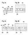
- a grid may be fabricated on porous silicon 845 by selectively growing an n-doped Si epitaxial layer 840 onto a patterned SiO 2 or Si 3 N 4 mask 835.
- the SiO 2 or Si 3 N 4 mask 835 acts in such a passivating manner that the monocrystalline silicon 840 can only grow on the exposed Si substrate 830, that is to say between the oxide or nitride regions 835, as shown in FIG FIG. 10b is shown.
- a porous region 845 are generated in the substrate 830, which can be converted into a cavern in a subsequent annealing process.
- FIG. 12a shows, for example, the simultaneous use of two different rectangular geometries.
- a second monocrystalline grid 890 or 895 is superposed with thicker webs.
- Such a combination may allow for both additional local membrane stiffening and increased membrane containment in the substrate 850.
- multiple implantations with appropriate masking and varying implantation energies can produce virtually any grid cross-sectional profile.
Landscapes
- Engineering & Computer Science (AREA)
- Mechanical Engineering (AREA)
- Microelectronics & Electronic Packaging (AREA)
- Computer Hardware Design (AREA)
- Manufacturing & Machinery (AREA)
- Pressure Sensors (AREA)
- Measuring Fluid Pressure (AREA)
- Weting (AREA)
Applications Claiming Priority (3)
| Application Number | Priority Date | Filing Date | Title |
|---|---|---|---|
| DE10358859 | 2003-12-16 | ||
| DE102004036032A DE102004036032A1 (de) | 2003-12-16 | 2004-07-24 | Verfahren zur Herstellung eines Halbleiterbauelements sowie ein Halbleiterbauelement, insbesondere ein Membransensor |
| EP04105448.7A EP1544163B1 (fr) | 2003-12-16 | 2004-11-02 | Méthode de production d'un capteur à membrane et capteur à membrane correspondant |
Related Parent Applications (2)
| Application Number | Title | Priority Date | Filing Date |
|---|---|---|---|
| EP04105448.7A Division-Into EP1544163B1 (fr) | 2003-12-16 | 2004-11-02 | Méthode de production d'un capteur à membrane et capteur à membrane correspondant |
| EP04105448.7A Division EP1544163B1 (fr) | 2003-12-16 | 2004-11-02 | Méthode de production d'un capteur à membrane et capteur à membrane correspondant |
Publications (2)
| Publication Number | Publication Date |
|---|---|
| EP1967488A2 true EP1967488A2 (fr) | 2008-09-10 |
| EP1967488A3 EP1967488A3 (fr) | 2008-09-17 |
Family
ID=34609489
Family Applications (1)
| Application Number | Title | Priority Date | Filing Date |
|---|---|---|---|
| EP08104525A Withdrawn EP1967488A3 (fr) | 2003-12-16 | 2004-11-02 | Méthode de production de dispositif semi-conducteur et dispositif semi-conducteur, plus particulièrement capteur à membrane |
Country Status (5)
| Country | Link |
|---|---|
| US (1) | US7843025B2 (fr) |
| EP (1) | EP1967488A3 (fr) |
| DE (2) | DE102004036035B4 (fr) |
| FR (1) | FR2863603B1 (fr) |
| IT (1) | ITMI20042393A1 (fr) |
Families Citing this family (43)
| Publication number | Priority date | Publication date | Assignee | Title |
|---|---|---|---|---|
| DE102004043356A1 (de) | 2004-09-08 | 2006-03-09 | Robert Bosch Gmbh | Sensorelement mit getrenchter Kaverne |
| DE102004043357B4 (de) * | 2004-09-08 | 2015-10-22 | Robert Bosch Gmbh | Verfahren zur Herstellung eines mikromechanischen Sensorelements |
| DE102005042648B4 (de) * | 2005-09-08 | 2007-06-21 | Robert Bosch Gmbh | Verfahren zur Herstellung von kommunizierenden Hohlräumen |
| DE102005060855A1 (de) | 2005-12-20 | 2007-06-28 | Robert Bosch Gmbh | Mikromechanischer kapazitiver Druckwandler und Herstellungsverfahren |
| DE102006009076A1 (de) * | 2006-02-28 | 2007-08-30 | Robert Bosch Gmbh | Verfahren und Vorrichtung zur Erkennung des freien Falls |
| DE102006012857A1 (de) | 2006-03-21 | 2007-09-27 | Robert Bosch Gmbh | Verfahren zur Herstellung einer Halbleiterstruktur und entsprechende Halbleiterstruktur |
| DE102006028435A1 (de) | 2006-06-21 | 2007-12-27 | Robert Bosch Gmbh | Sensor und Verfahren zu seiner Herstellung |
| DE102007002273A1 (de) | 2007-01-16 | 2008-07-17 | Robert Bosch Gmbh | Verfahren zur Herstellung eines Bauteils und Sensorelement |
| DE102007003544A1 (de) | 2007-01-24 | 2008-07-31 | Robert Bosch Gmbh | Verfahren zur Herstellung eines Bauteils und Sensorelement |
| DE102007019647A1 (de) | 2007-04-26 | 2008-10-30 | Robert Bosch Gmbh | Verfahren zur Herstellung eines mikromechanischen Bauelements mit Auffüllschicht und Maskenschicht |
| DE102007019639A1 (de) | 2007-04-26 | 2008-10-30 | Robert Bosch Gmbh | Mikromechanisches Bauelement und entsprechendes Herstellungsverfahren |
| DE102007024199B4 (de) * | 2007-05-24 | 2015-06-25 | Robert Bosch Gmbh | Herstellungsverfahren eines mikromechanischen Bauelements mit porösifizierter Membran |
| DE102007052663A1 (de) | 2007-11-05 | 2009-05-07 | Robert Bosch Gmbh | Mikromechanisches Bauelement, Kurzprozess zur Herstellung von MEMS-Bauelementen |
| DE102007053280A1 (de) | 2007-11-08 | 2009-05-14 | Robert Bosch Gmbh | Mikromechanisches Bauelement mit einem Membrangitter |
| DE102008001185A1 (de) | 2008-04-15 | 2009-10-29 | Robert Bosch Gmbh | Verfahren zur Herstellung einer mikromechanischen Membranstruktur mit feststehendem Gegenelement |
| DE102008002332B4 (de) | 2008-06-10 | 2017-02-09 | Robert Bosch Gmbh | Verfahren zur Herstellung einer mikromechanischen Membranstruktur mit Zugang von der Substratrückseite |
| DE102008002668A1 (de) | 2008-06-26 | 2009-12-31 | Robert Bosch Gmbh | Mikromechanisches Bauelement und entsprechendes Herstellungsverfahren |
| DE102008040521A1 (de) | 2008-07-18 | 2010-01-21 | Robert Bosch Gmbh | Verfahren zur Herstellung eines Bauelements, Verfahren zur Herstellung einer Bauelementanordnung, Bauelement und Bauelementanordnung |
| DE102008041942A1 (de) | 2008-09-10 | 2010-03-11 | Robert Bosch Gmbh | Sensoranordnung, Verfahren zum Betrieb einer Sensoranordnung und Verfahren zur Herstellung einer Sensoranordnung |
| DE102008043382B4 (de) * | 2008-11-03 | 2017-01-19 | Robert Bosch Gmbh | Bauelement und Verfahren zu dessen Herstellung |
| DE102009027180A1 (de) | 2009-06-25 | 2010-12-30 | Robert Bosch Gmbh | Mikromechanisches Element sowie Verfahren zu dessen Herstelllung |
| DE102009045158A1 (de) | 2009-09-30 | 2011-04-07 | Robert Bosch Gmbh | Sensoranordnung und Verfahren zur Herstellung einer Sensoranordnung |
| DE102010002818B4 (de) | 2010-03-12 | 2017-08-31 | Robert Bosch Gmbh | Verfahren zur Herstellung eines mikromechanischen Bauelementes |
| US20120062570A1 (en) * | 2010-09-10 | 2012-03-15 | Qualcomm Mems Technologies, Inc. | Process of forming an air gap in a microelectromechanical system device using a liner material |
| DE102010041101B4 (de) | 2010-09-21 | 2018-05-30 | Robert Bosch Gmbh | Bauelement mit einer Durchkontaktierung und ein Verfahren zur Herstellung eines Bauelements mit einer Durchkontaktierung |
| DE102012109587A1 (de) * | 2012-10-09 | 2014-04-10 | Endress + Hauser Gmbh + Co. Kg | Differenzdrucksensor und Verfahren zu seiner Herstellung |
| DE102013211970A1 (de) | 2013-06-25 | 2015-01-22 | Robert Bosch Gmbh | Mikro-elektromechanischer Resonator und Verfahren zum Herstellen eines mikro-elektromechanischen Resonators |
| DE102013217349B4 (de) | 2013-08-30 | 2024-06-13 | Robert Bosch Gmbh | Mikromechanische Sensoranordnung und entsprechendes Herstellungsverfahren |
| DE102014207480A1 (de) | 2014-04-17 | 2015-10-22 | Robert Bosch Gmbh | Vorrichtung zum Erfassen eines Parameters eines Gases, Verfahren zum Betreiben einer derartigen Vorrichtung und Messsystem zum Bestimmen eines Parameters eines Gases |
| DE102014214525B4 (de) | 2014-07-24 | 2019-11-14 | Robert Bosch Gmbh | Mikro-elektromechanisches Bauteil und Herstellungsverfahren für mikro-elektromechanische Bauteile |
| US9212045B1 (en) * | 2014-07-31 | 2015-12-15 | Infineon Technologies Ag | Micro mechanical structure and method for fabricating the same |
| US10081533B2 (en) | 2014-07-31 | 2018-09-25 | Infineon Technologies Ag | Micromechanical structure and method for fabricating the same |
| US9805931B2 (en) * | 2015-08-28 | 2017-10-31 | Varian Semiconductor Equipment Associates, Inc. | Liquid immersion doping |
| DE102016201144B4 (de) | 2016-01-27 | 2024-05-23 | Robert Bosch Gmbh | Halbleitersensor für eine Gaskonzentration |
| DE102016216870B4 (de) | 2016-09-06 | 2019-07-18 | Robert Bosch Gmbh | Verfahren zum Herstellen eines mikromechanischen Bauteils mit einer freigestellten Drucksensoreinrichtung |
| DE102016219807B4 (de) | 2016-10-12 | 2025-05-15 | Robert Bosch Gmbh | Mikromechanischer Sensor |
| DE102017209306A1 (de) | 2017-06-01 | 2018-12-06 | Robert Bosch Gmbh | Vorrichtung zum Schutz von Bauteilen |
| DE102017209313B4 (de) | 2017-06-01 | 2022-02-10 | Robert Bosch Gmbh | Vorrichtung zum Schutz von Bauteilen vor Flüssigkeiten und zu deren Belüftung sowie Verfahren zu dessen Herstellung |
| DE102017212866A1 (de) | 2017-07-26 | 2019-01-31 | Robert Bosch Gmbh | Drucksensoranordnung, Messvorrichtung und Verfahren zu deren Herstellung |
| DE102017212838B4 (de) | 2017-07-26 | 2024-08-22 | Robert Bosch Gmbh | Drucksensoranordnung, Messvorrichtung und Verfahren zu deren Herstellung |
| DE102018222724A1 (de) * | 2018-12-21 | 2020-06-25 | Robert Bosch Gmbh | Verfahren zum Herstellen einer dreidimensional stressentkoppelten Substratanordnung |
| DE102020211230A1 (de) | 2020-09-08 | 2021-08-19 | Robert Bosch Gesellschaft mit beschränkter Haftung | Mikromechanisches Drucksensorelement und Verfahren zum Herstellen eines mikromechanischen Drucksensorelements |
| DE102020215985A1 (de) | 2020-12-16 | 2022-06-23 | Robert Bosch Gesellschaft mit beschränkter Haftung | Mikromechanisches Bauteil für eine kapazitive Drucksensorvorrichtung, kapazitive Drucksensorvorrichtung und ein Herstellungsverfahren für eine kapazitive Drucksensorvorrichtung |
Citations (2)
| Publication number | Priority date | Publication date | Assignee | Title |
|---|---|---|---|---|
| DE10030352A1 (de) | 2000-06-21 | 2002-01-10 | Bosch Gmbh Robert | Mikromechanisches Bauelement, insbesondere Sensorelement, mit einer stabilisierten Membran und Verfahren zur Herstellung eines derartigen Bauelements |
| DE10138759A1 (de) | 2001-08-07 | 2003-03-06 | Bosch Gmbh Robert | Verfahren zur Herstellung eines Halbleiterbauelements sowie Halbleiterbauelement, insbesondere Membransensor |
Family Cites Families (9)
| Publication number | Priority date | Publication date | Assignee | Title |
|---|---|---|---|---|
| US4766666A (en) | 1985-09-30 | 1988-08-30 | Kabushiki Kaisha Toyota Chuo Kenkyusho | Semiconductor pressure sensor and method of manufacturing the same |
| CN1018844B (zh) * | 1990-06-02 | 1992-10-28 | 中国科学院兰州化学物理研究所 | 防锈干膜润滑剂 |
| FR2700003B1 (fr) | 1992-12-28 | 1995-02-10 | Commissariat Energie Atomique | Procédé de fabrication d'un capteur de pression utilisant la technologie silicium sur isolant et capteur obtenu. |
| KR0155141B1 (ko) | 1993-12-24 | 1998-10-15 | 손병기 | 다공질실리콘을 이용한 반도체 장치의 제조방법 |
| DE69935495T2 (de) * | 1999-04-29 | 2007-11-29 | Stmicroelectronics S.R.L., Agrate Brianza | Herstellungsverfahren für vergrabene Kanäle und Hohlräume in Halbleiterscheiben |
| DE10032579B4 (de) * | 2000-07-05 | 2020-07-02 | Robert Bosch Gmbh | Verfahren zur Herstellung eines Halbleiterbauelements sowie ein nach dem Verfahren hergestelltes Halbleiterbauelement |
| DE10054484A1 (de) * | 2000-11-03 | 2002-05-08 | Bosch Gmbh Robert | Mikromechanisches Bauelement und entsprechendes Herstellungsverfahren |
| ITVA20000042A1 (it) | 2000-12-15 | 2002-06-15 | St Microelectronics Srl | Sensore di pressione monoliticamente integrato e relativo processo direalizzazione. |
| EP1306348B1 (fr) * | 2001-10-24 | 2007-05-16 | Robert Bosch Gmbh | Procédé de fabrication d'une unité capteuse à mémbrane et unité capteuse à mémbrane |
-
2004
- 2004-07-24 DE DE102004036035.9A patent/DE102004036035B4/de not_active Expired - Lifetime
- 2004-07-24 DE DE102004036032A patent/DE102004036032A1/de not_active Withdrawn
- 2004-11-02 EP EP08104525A patent/EP1967488A3/fr not_active Withdrawn
- 2004-12-15 FR FR0452986A patent/FR2863603B1/fr not_active Expired - Fee Related
- 2004-12-15 IT IT002393A patent/ITMI20042393A1/it unknown
-
2009
- 2009-01-26 US US12/359,904 patent/US7843025B2/en not_active Expired - Lifetime
Patent Citations (2)
| Publication number | Priority date | Publication date | Assignee | Title |
|---|---|---|---|---|
| DE10030352A1 (de) | 2000-06-21 | 2002-01-10 | Bosch Gmbh Robert | Mikromechanisches Bauelement, insbesondere Sensorelement, mit einer stabilisierten Membran und Verfahren zur Herstellung eines derartigen Bauelements |
| DE10138759A1 (de) | 2001-08-07 | 2003-03-06 | Bosch Gmbh Robert | Verfahren zur Herstellung eines Halbleiterbauelements sowie Halbleiterbauelement, insbesondere Membransensor |
Also Published As
| Publication number | Publication date |
|---|---|
| US7843025B2 (en) | 2010-11-30 |
| US20090127640A1 (en) | 2009-05-21 |
| DE102004036035A1 (de) | 2005-07-21 |
| FR2863603B1 (fr) | 2007-06-08 |
| ITMI20042393A1 (it) | 2005-03-15 |
| FR2863603A1 (fr) | 2005-06-17 |
| DE102004036035B4 (de) | 2015-10-15 |
| EP1967488A3 (fr) | 2008-09-17 |
| DE102004036032A1 (de) | 2005-07-21 |
Similar Documents
| Publication | Publication Date | Title |
|---|---|---|
| DE102004036035B4 (de) | Verfahren zur Herstellung eines Halbleiterbauelements sowie ein Halbleiterbauelement, insbesondere ein Membransensor | |
| DE10063991B4 (de) | Verfahren zur Herstellung von mikromechanischen Bauelementen | |
| DE10032579B4 (de) | Verfahren zur Herstellung eines Halbleiterbauelements sowie ein nach dem Verfahren hergestelltes Halbleiterbauelement | |
| EP1423330B1 (fr) | Composant semi-conducteur, notamment detecteur a membrane, et son procédé de production. | |
| EP1345842B1 (fr) | Procédé de production d'un composant semi-conducteur et composant semi-conducteur produit selon ce procédé et ayant notamment une masse mobile | |
| EP1167934A1 (fr) | Composant micromécanique, en particulier élément capteur, ayant une membrane stabilisée et procédé pour le produire | |
| WO2009149980A2 (fr) | Procédé pour produire une structure membranaire micro-mécanique comportant un accès par le côté arrière du substrat | |
| EP2002475B1 (fr) | Procédé pour produire un circuit intégré | |
| DE19843984B4 (de) | Verfahren zur Herstellung von Strahlungssensoren | |
| EP1544163B1 (fr) | Méthode de production d'un capteur à membrane et capteur à membrane correspondant | |
| US7755152B2 (en) | Semiconductor component configured as a diaphragm sensor | |
| EP1347937A2 (fr) | Composant micromecanique et procede de production correspondant | |
| EP1597193B1 (fr) | Procede de fabrication d'un composant comportant un support a semiconducteurs | |
| DE10046622B4 (de) | Verfahren zur Herstellung einer Membransensoreinheit sowie Membransensoreinheit | |
| EP1306348B1 (fr) | Procédé de fabrication d'une unité capteuse à mémbrane et unité capteuse à mémbrane | |
| DE10046621A1 (de) | Verfahren zur Herstellung eines Membransensor-Arrays sowie Membransensor-Array | |
| EP1546027A2 (fr) | Procede et composant micromecanique | |
| DE102005009422B4 (de) | Mikromechanisches Bauelement und entsprechendes Herstellungsverfahren | |
| DE102006059394B4 (de) | Integrierte Schaltung und Verfahren zu deren Herstellung | |
| DE102006013419B4 (de) | Verfahren zum Herstellen einer integrierten Schaltung | |
| EP1306349B1 (fr) | Procédé de fabrication d'une série de capteurs à membrane et série de capteurs à membrane | |
| DE102007024199B4 (de) | Herstellungsverfahren eines mikromechanischen Bauelements mit porösifizierter Membran |
Legal Events
| Date | Code | Title | Description |
|---|---|---|---|
| PUAI | Public reference made under article 153(3) epc to a published international application that has entered the european phase |
Free format text: ORIGINAL CODE: 0009012 |
|
| PUAL | Search report despatched |
Free format text: ORIGINAL CODE: 0009013 |
|
| AC | Divisional application: reference to earlier application |
Ref document number: 1544163 Country of ref document: EP Kind code of ref document: P |
|
| AK | Designated contracting states |
Kind code of ref document: A2 Designated state(s): DE FR IT |
|
| AK | Designated contracting states |
Kind code of ref document: A3 Designated state(s): DE FR IT |
|
| 17P | Request for examination filed |
Effective date: 20090317 |
|
| AKX | Designation fees paid |
Designated state(s): DE FR IT |
|
| 17Q | First examination report despatched |
Effective date: 20090622 |
|
| STAA | Information on the status of an ep patent application or granted ep patent |
Free format text: STATUS: THE APPLICATION IS DEEMED TO BE WITHDRAWN |
|
| 18D | Application deemed to be withdrawn |
Effective date: 20140903 |