EP1967871A2 - Filter und Anzeigevorrichtung damit - Google Patents
Filter und Anzeigevorrichtung damit Download PDFInfo
- Publication number
- EP1967871A2 EP1967871A2 EP08250788A EP08250788A EP1967871A2 EP 1967871 A2 EP1967871 A2 EP 1967871A2 EP 08250788 A EP08250788 A EP 08250788A EP 08250788 A EP08250788 A EP 08250788A EP 1967871 A2 EP1967871 A2 EP 1967871A2
- Authority
- EP
- European Patent Office
- Prior art keywords
- color patterns
- filter according
- filter
- base film
- color
- Prior art date
- Legal status (The legal status is an assumption and is not a legal conclusion. Google has not performed a legal analysis and makes no representation as to the accuracy of the status listed.)
- Withdrawn
Links
Images
Classifications
-
- G—PHYSICS
- G02—OPTICS
- G02B—OPTICAL ELEMENTS, SYSTEMS OR APPARATUS
- G02B5/00—Optical elements other than lenses
- G02B5/20—Filters
-
- H—ELECTRICITY
- H01—ELECTRIC ELEMENTS
- H01J—ELECTRIC DISCHARGE TUBES OR DISCHARGE LAMPS
- H01J11/00—Gas-filled discharge tubes with alternating current induction of the discharge, e.g. alternating current plasma display panels [AC-PDP]; Gas-filled discharge tubes without any main electrode inside the vessel; Gas-filled discharge tubes with at least one main electrode outside the vessel
- H01J11/20—Constructional details
- H01J11/34—Vessels, containers or parts thereof, e.g. substrates
- H01J11/44—Optical arrangements or shielding arrangements, e.g. filters, black matrices, light reflecting means or electromagnetic shielding means
-
- G—PHYSICS
- G02—OPTICS
- G02B—OPTICAL ELEMENTS, SYSTEMS OR APPARATUS
- G02B5/00—Optical elements other than lenses
- G02B5/20—Filters
- G02B5/201—Filters in the form of arrays
-
- G—PHYSICS
- G02—OPTICS
- G02B—OPTICAL ELEMENTS, SYSTEMS OR APPARATUS
- G02B5/00—Optical elements other than lenses
- G02B5/20—Filters
- G02B5/208—Filters for use with infrared or ultraviolet radiation, e.g. for separating visible light from infrared and/or ultraviolet radiation
-
- H—ELECTRICITY
- H01—ELECTRIC ELEMENTS
- H01J—ELECTRIC DISCHARGE TUBES OR DISCHARGE LAMPS
- H01J11/00—Gas-filled discharge tubes with alternating current induction of the discharge, e.g. alternating current plasma display panels [AC-PDP]; Gas-filled discharge tubes without any main electrode inside the vessel; Gas-filled discharge tubes with at least one main electrode outside the vessel
- H01J11/10—AC-PDPs with at least one main electrode being out of contact with the plasma
-
- H—ELECTRICITY
- H01—ELECTRIC ELEMENTS
- H01J—ELECTRIC DISCHARGE TUBES OR DISCHARGE LAMPS
- H01J2211/00—Plasma display panels with alternate current induction of the discharge, e.g. AC-PDPs
- H01J2211/20—Constructional details
- H01J2211/34—Vessels, containers or parts thereof, e.g. substrates
- H01J2211/44—Optical arrangements or shielding arrangements, e.g. filters or lenses
- H01J2211/442—Light reflecting means; Anti-reflection means
-
- H—ELECTRICITY
- H01—ELECTRIC ELEMENTS
- H01J—ELECTRIC DISCHARGE TUBES OR DISCHARGE LAMPS
- H01J2211/00—Plasma display panels with alternate current induction of the discharge, e.g. AC-PDPs
- H01J2211/20—Constructional details
- H01J2211/34—Vessels, containers or parts thereof, e.g. substrates
- H01J2211/44—Optical arrangements or shielding arrangements, e.g. filters or lenses
- H01J2211/444—Means for improving contrast or colour purity, e.g. black matrix or light shielding means
-
- Y—GENERAL TAGGING OF NEW TECHNOLOGICAL DEVELOPMENTS; GENERAL TAGGING OF CROSS-SECTIONAL TECHNOLOGIES SPANNING OVER SEVERAL SECTIONS OF THE IPC; TECHNICAL SUBJECTS COVERED BY FORMER USPC CROSS-REFERENCE ART COLLECTIONS [XRACs] AND DIGESTS
- Y10—TECHNICAL SUBJECTS COVERED BY FORMER USPC
- Y10T—TECHNICAL SUBJECTS COVERED BY FORMER US CLASSIFICATION
- Y10T428/00—Stock material or miscellaneous articles
- Y10T428/24—Structurally defined web or sheet [e.g., overall dimension, etc.]
- Y10T428/24802—Discontinuous or differential coating, impregnation or bond [e.g., artwork, printing, retouched photograph, etc.]
Definitions
- the present invention relates to a filter and a plasma display apparatus including the same, and more particularly, to a filter which provides excellent bright room contrast by transmitting internal light and blocking external light, and can be produced in lightweight thin films at low cost and a plasma display apparatus including the same
- a plasma display apparatus using a plasma display panel is a flat display device which displays images using a gas discharge principle, and has excellent display capability in terms of brightness, contrast, after image, and viewing angle, compared to a conventional cathode-ray tube (CRT).
- plasma display apparatuses can be made in thin films with large sizes. Due to these advantages, plasma display apparatuses are regarded as a next-generation large-size flat display apparatus.
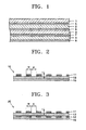
- FIG. 1 is a cross-sectional view of part of a conventional tempered glass filter of a plasma display apparatus.
- the conventional tempered glass filter includes an anti-reflective layer 1, a heat-treated tempered glass 2, an etching mesh film 3, and a near infrared-absorbing film 4, and adhesive layers 5, 6, 7, and 8 interposed between respective layers.
- the tempered glass filter has a thickness of about 3 mm so that it can endure external impacts, and thus, the weight of the filter is increased and its manufacturing cost increases.
- the conventional tempered glass filter has a very complex structure formed of many functional films, and thus the manufacturing process is complex and expensive.
- the conventional tempered glass filter cannot sufficiently improve a bright room contrast, and even when the bright room contrast can be improved, brightness is significantly reduced. Accordingly, there is a need to solve these problems.
- the present invention sets out to provide a filter which reduces the decrease in brightness, improves bright room contrast, and is more lightweight, and a display apparatus including the same.
- the present invention also sets out to provide a filter which can be easily manufactured at low cost, and a display apparatus including the same.
- a filter including: a base film; and a plurality of first color patterns extending in a predetermined direction and disposed at predetermined intervals in a stripe form on a surface of the base film.
- a width of a cross section of each of the first color patterns may be substantially identical to or smaller than an interval between adjacent first color patterns.
- the width of the cross section of each of the first color patterns may be in the range of 5 ⁇ m to 50 ⁇ m.
- the thickness of the cross section of each of the first color patterns may be in the range of 1 ⁇ m to 200 ⁇ m.
- a ratio of the thickness to the interval between adjacent first color patterns may be in the range of 0.025 to 50.
- the filter may further include an adhesive layer disposed on a rear surface of the base film.
- the filter may further includes a plurality of second color patterns extending in a predetermined direction and disposed at predetermined intervals in a stripe form on an opposite surface of the base film to the surface on which the first color patterns are disposed.
- the second color patterns may be disposed in substantially corresponding locations to the first color patterns.
- the misalignment of the first color pattern and the second color patterns may be in the range of 0% to 20 %, wherein 0% of the misalignment indicates exact overlapping of the first color pattern and the second color pattern.
- Widths of the first and second color patterns are substantially the same as intervals of the first and second color patterns on the base film.
- the width of a cross section of each of the first and second color patterns may be in the range of 5 ⁇ m to 60 ⁇ m.
- the thickness of a cross section of each of the first and second color patterns may be in the range of 1 ⁇ m to 200 ⁇ m.
- a ratio of the thickness to the width may be in the range of 0.025 to 60.
- the filter may further include an adhesive layer which fills intervals between a rear surface of the base film and the second color patterns.
- the base film includes dyes or pigment to adjust color and transmissivity.
- a display apparatus including: a display panel which displays an image; an operation circuit substrate which controls the display panel by supplying an operation signal and electrical power to the display panel; a chassis supporting the display panel and the operation circuit substrate; and the filter bonding to a front surface of the display panel.
- the display apparatus may be a plasma display panel which displays images through gas discharge.
- a first aspect of the invention provides a filter as set out in Claim 1. Preferred features of this aspect of the invention are set out in Claims 2 to 15. A second aspect of the invention provides a display apparatus as set out in Claim 16. Preferred features of this aspect of the invention are set out in Claim 17.
- FIG. 1 is a cross-sectional view of part of a conventional filter
- FIG. 2 is a schematic cross-sectional view of part of a filter according to an embodiment of the present invention.
- FIG. 3 is a schematic cross-sectional view of part of a filter according to another embodiment of the present invention.
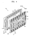
- FIG. 4 is an exploded perspective view of a display apparatus including the filter according to an embodiment of the present invention.
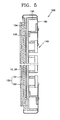
- FIG. 5 is a cross-sectional view of the display apparatus of FIG. 4 , taken along line V-V.
- FIG. 2 is a schematic cross-sectional view of part of a filter 10 according to an embodiment of the present invention.
- the filter 10 includes a plurality of color patterns 11 and a base film 13.
- the color patterns 11 are disposed at predetermined intervals in a stripe form on the base film 13.
- the color patterns 11 are formed of a material that has a high absorption rate with respect to visible light.
- the color patterns 11 may be black.
- the color patterns 11 are substantially disposed at constant intervals in order to obtain a uniform external light reflection decrease effect in the entire screen.
- w denotes the width of a cross section of the color patterns 11
- d denotes the interval between adjacent color patterns 11
- w ⁇ d ⁇ 95 w .
- the aperture rate is 50%.
- the transmissivity rate of the filter is lowered and thus the brightness of the display device is decreased.
- the distance (d) of the color patterns 11 may be 95 times or less greater than the width (w) of the cross section of the color patterns 11 so that the aperture rate is 95% or less.
- the aperture rate is more than 95%, the external light reflection decrease effect of the filter is substantially decreased and the bright room contrast improvement effect is substantially decreased.
- a cross section of each color pattern 11 may have a width (w) of 5 ⁇ m to 50 ⁇ m and a thickness (t) of 1 ⁇ m to 200 ⁇ m.
- the width (w) may be 0.025 to 50 times larger than the thickness (t).
- a display device to which the filter according to an embodiment of the present invention is applied may have a very narrow viewing angle.
- the thickness (t) of the color patterns 11 is less than 1 ⁇ m, the bright room contrast improvement effect of the filter may be substantially decreased.
- the base film 13 is formed of a material through which visible light can propagate.
- the base film 13 bonds the filter 10 directly to a front surface of a display apparatus.
- the base film 13 can be formed of any transparent material that is easily, tightly attached to glass or plastic in view of interface characteristics.
- the base film 13 can be formed of a flexible material for easy transportation and to simplify an attaching process and make transportation easy.
- the interface characteristics of the base film forming material may be less relevant.
- the base film 13 may be formed of polyethersulphone (PES), polyacrylate (PAR), polyetherimide (PEI), polyethyelenen napthalate (PEN), polyethyeleneterepthalate (PET), polyphenylene sulfide (PPS), polyallylate, polyimide, polycarbonate (PC), cellulose tri acetate (TAC), cellulose acetate propinonate (CAP), or the like.
- PES polyethersulphone
- PAR polyacrylate
- PEI polyetherimide
- PEN polyethyelenen napthalate
- PET polyethyeleneterepthalate
- PPS polyphenylene sulfide
- polyallylate polyimide
- PC polycarbonate
- TAC cellulose tri acetate
- CAP cellulose acetate propinonate
- the base film 13 can be colored with a predetermined color. Accordingly, the transmissivity of visible light with respect to the filter 10 can be adjusted by controlling coloring conditions of the base film 13. For example, when the base film 13 has a dark color, the transmissivity of visible light may decrease. In addition, the color of visible light which propagates in the forward direction from a display apparatus can be controlled. That is, the base film 13 can be colored such that a user is visibly satisfied, or colored to improve color purity of a display apparatus including the filter 10. Furthermore, the base film 13 has color patterns corresponding to respective sub pixels of a plasma display panel to which the filter 10 is applied. It will be appreciated that the base film 13 may be colored in various ways for a variety of color correction purposes.
- the base film 13 have a thickness of 50 ⁇ m to 500 ⁇ m, preferably 80 ⁇ m to 400 ⁇ m. When the base film 13 is thin, the effects of preventing scattering of pieces when the panel is destroyed may be decreased. On the other hand, when the base film 13 is thick, the efficiency of the laminating process may be decreased.
- an adhesive layer 15 can be disposed on a rear surface of the base film 13 in order to bind the filter 10 to a front surface of the display apparatus.
- the difference in the refraction rates of the adhesive layer 15 and the display panel may be adjusted to a predetermined value, such as 1.0% or less, to decrease a double image phenomenon.
- the adhesive layer 15 may include a thermoplastic or UV thermosetting resin.
- the adhesive layer 15 may include an acryl resin, pressure sensitive adhesive (PSA).
- PSA pressure sensitive adhesive
- the adhesive layer 15 can be formed by dip coating, air knife coating, roller coating, wire bar coating, or gravure coating.
- the adhesive layer 15 may further include a compound that absorbs near infrared light, such as a copper atom-containing resin, a copper compound or phosphor compound-containing resin, a copper compound or THIO derivative-containing resin, a tungsten-based compound-containing resin, or a cyanine-based compound-containing resin.
- a compound that absorbs near infrared light such as a copper atom-containing resin, a copper compound or phosphor compound-containing resin, a copper compound or THIO derivative-containing resin, a tungsten-based compound-containing resin, or a cyanine-based compound-containing resin.
- the adhesive layer 15 may further include a coloring agent, such as a dye or pigment, to block neon light for color correction.
- the coloring agent selectively absorbs light of the visible light region having a wavelength of 400 - 700 nm.
- a neon gas acting as a discharge gas generates unnecessary visible light with a wavelength of about 585 nm.
- a cyanine-based, squarylium-based, azomethine-based, xanthene-based, oxonol-based, or azo-based compound is used to absorb the unnecessary visible light.
- These coloring agents are included in the adhesive layer 15 in a dispersed micro particle form.
- FIG. 3 is a schematic cross-sectional view of part of a filter 20 according to another embodiment of the present invention.
- the filter 20 includes a plurality of first color patterns 11, a plurality of second color patterns 12, and a base film 13.
- the first color patterns 11 are disposed at predetermined intervals in a strip form on a surface of the base film 13.
- the second color patterns 12 are disposed at predetermined intervals in a strip form on another surface of the base film 13, that is, on an opposite surface of base film 13 to the surface on which the first color patterns 12 are disposed.
- the first color patterns 11 and the second color patterns 12 are formed of a material that has a high absorption rate with respect to visible light.
- the first color patterns 11 and the second color patterns 12 may be black.
- the first color patterns 11 and the second color patterns 12 may be substantially disposed at constant intervals in order to obtain a uniform external light reflection decrease effect in the entire screen.
- w denotes widths of the first color patterns 11 and the second color patterns 12
- d denotes the interval between adjacent first color patterns 11 and the interval between adjacent second color patterns 12
- w ⁇ d ⁇ 95 w denotes widths of the first color patterns 11 and the second color patterns 12
- the aperture rate is 50%.
- the transmissivity rate of the filter is lowered and thus the brightness of the display device is decreased.
- the distances (d) of the first color patterns 11 and the second color patterns 12 may be 95 times or less greater than the widths (w) of the first color patterns 11 and the second color patterns 12 so that the aperture rate is 95% or less.
- the aperture rate is more than 95%, the external light reflection decrease effect of the filter is substantially decreased and the bright room contrast improvement effect is substantially decreased:
- the first color patterns 11 may be disposed in substantially corresponding locations to the second color patterns 12 wherein the first color patterns 11 and the second color patterns 12 are disposed on opposite surfaces of the base film 13.
- the misalignment of the first color pattern and the second color patterns may be 20 % or less of widths of cross sections of the first color patterns 11 and the second color patterns 12. When the misalignment is 20% or more, the aperture rate is low and the external light reflection decrease effect is decreased.
- a cross section of each of the first color patterns 11 and the second color patterns 12 may have a width (w) of 5 ⁇ m to 60 ⁇ m and a thickness (t) of 1 to 200 ⁇ m.
- the width (w) may be 0.025 to 60 times larger than the thickness (t).
- a display device to which the filter according to an embodiment of the present invention is applied may have a very narrow viewing angle.
- the thickness (t) of each of the first color patterns 11 and the second color patterns 12 is less than 1 ⁇ m, the bright room contrast improvement effect of the filter may be substantially decreased.
- the base film 13 may be formed of a material through which visible light propagates, and directly binds the filter 20 to a front surface of the display apparatus, as described in the previous embodiment.
- an adhesive layer is used as described above, there is no need to consider the adhesive properties of the base film 13 with respect to the front surface of the display apparatus.
- the intervals between the second color patterns and the intervals between the outer surface of the adhesive layer 16 and the surfaces of the second color patterns 12 may be entirely filled, and other features are the same as described in the previous embodiment.
- Table 1 shows measurement results according to a comparative embodiment and the current embodiment of the present invention.
- the unit of brightness is cd/m 2 .
- the line width of a color pattern is 80 ⁇ m
- the thickness of a film is 175 ⁇ m
- the interval between color patterns is 80 ⁇ m
- the aperture rate is 50%.
- Table 1 Transmissivity Peak Brightness External Light Reflection Brightness Contrast Ratio Comparative Embodiment 39% 546 1.772 308:1 Current Embodiment 39% 546 1.370 398:1
- the filter according to the current embodiment of the present invention and the filter according to a comparative embodiment have the same transmissivity.
- the filter according to the current embodiment of the present invention shows lower external light reflection brightness and thus the bright room contrast can be improved by about 23%.
- FIG. 4 is a perspective view of a plasma display apparatus 100 including an filter according to an embodiment of the present invention
- FIG. 5 is a cross-sectional view of the display apparatus of FIG. 4 , taken along the line V-V.
- the filter according to the present invention is used in a plasma display apparatus.
- a display apparatus including a filter according to an embodiment of the present invention is not limited to being a plasma display apparatus.
- the plasma display apparatus 100 includes a plasma display panel 150, a chassis 130, and a circuit unit 140.
- the filter 10 or 20 is attached to a front surface of the plasma display panel 150.
- the plasma display panel 150 can bond to the chassis 130 through an adhesive, such as a double-side tape 154.
- a thermally conductive member 153 may be interposed between the chassis 130 and the plasma display panel 150 to dissipate heat which is generated when the plasma display panel 150 operates through the chassis 130.
- the plasma display panel 150 displays an image through gas discharge, and includes a front panel 151 and a rear panel 152 combined together.
- the filter 10 or 20 can be bound to the front surface of the plasma display panel 150 by an adhesive layer (not shown.)
- the filter 10 or 20 allows internal visible light generated in the plasma display panel 150 to propagate in a forward direction from the plasma display apparatus 100 and reflects or blocks external light, so that the bright room contrast of the plasma display panel 150 improves.
- substantially direct bonding of the filter 10 to the front surface of the plasma display panel 150 prevents the occurrence of double images.
- the filter 10 or 20 is more lightweight and its manufacturing costs and physical distribution costs are reduced.
- the chassis 130 is disposed at a rear side of the plasma display panel 150 to structurally support the plasma display panel 150.
- the chassis 130 may be formed of a metal having excellent rigidity, such as aluminum or iron, or plastic.
- a thermally conductive member 153 is interposed between the plasma display panel 150 and the chassis 130.
- the thermally conductive member 153 is surrounded by a plurality of pieces of double-sided tape 154 which fix the plasma display panel 150 and the chassis 130 together.
- a circuit unit 140 is disposed on a rear side of the chassis 130, and circuits which operate the plasma display panel 150 are arranged on the circuit unit 140.
- the circuit unit 140 carries an electrical signal to the plasma display panel 150 by signal carrying means.
- the signal carrying means can be flexible printed cable (FPC), tape carrier package (TCP), chip on film (COF), or the like.
- FPCs 161 used as signal carrying means are disposed at left and right sides of the chassis 130, and TCPs 160 used as signal carrying means are disposed at upper and lower sides of the chassis 130.
- the above described apparatus including a filter according to the present invention is a plasma display apparatus
- the filter can be attached to front surfaces of various other types of display apparatus.
- a filter according to the present invention and a plasma display apparatus including the same, formation of double images can be prevented because the filter is directly bound to a front surface of a display panel.
- the weight of the filter is decreased because the thickness of a base film used in the film is relatively thin.
- use of the filter contributes to improved bright room contrast.
Landscapes
- Physics & Mathematics (AREA)
- Engineering & Computer Science (AREA)
- Plasma & Fusion (AREA)
- General Physics & Mathematics (AREA)
- Optics & Photonics (AREA)
- Electromagnetism (AREA)
- Health & Medical Sciences (AREA)
- Toxicology (AREA)
- Devices For Indicating Variable Information By Combining Individual Elements (AREA)
- Optical Filters (AREA)
Applications Claiming Priority (1)
| Application Number | Priority Date | Filing Date | Title |
|---|---|---|---|
| KR1020070023174A KR20080082379A (ko) | 2007-03-08 | 2007-03-08 | 필터 및 이를 구비한 디스플레이 장치 |
Publications (2)
| Publication Number | Publication Date |
|---|---|
| EP1967871A2 true EP1967871A2 (de) | 2008-09-10 |
| EP1967871A3 EP1967871A3 (de) | 2009-07-29 |
Family
ID=39537917
Family Applications (1)
| Application Number | Title | Priority Date | Filing Date |
|---|---|---|---|
| EP08250788A Withdrawn EP1967871A3 (de) | 2007-03-08 | 2008-03-07 | Filter und Anzeigevorrichtung damit |
Country Status (5)
| Country | Link |
|---|---|
| US (1) | US20080220225A1 (de) |
| EP (1) | EP1967871A3 (de) |
| JP (1) | JP2008225433A (de) |
| KR (1) | KR20080082379A (de) |
| CN (1) | CN101261335A (de) |
Families Citing this family (4)
| Publication number | Priority date | Publication date | Assignee | Title |
|---|---|---|---|---|
| KR100937964B1 (ko) * | 2008-12-01 | 2010-01-21 | 삼성에스디아이 주식회사 | 디스플레이 장치 및 광학 필터 |
| CN103293580A (zh) * | 2011-12-31 | 2013-09-11 | 四川虹欧显示器件有限公司 | 滤光膜及包括其的显示屏 |
| KR102533255B1 (ko) * | 2016-06-01 | 2023-05-17 | 삼성디스플레이 주식회사 | 점착제 |
| CN113012565B (zh) * | 2019-12-18 | 2023-12-01 | 群创光电股份有限公司 | 可挠式显示装置 |
Family Cites Families (9)
| Publication number | Priority date | Publication date | Assignee | Title |
|---|---|---|---|---|
| US6255778B1 (en) * | 1997-10-13 | 2001-07-03 | Bridgestone Corporation | Plasma display panel having electromagnetic wave shielding material attached to front surface of display |
| US6086979A (en) * | 1997-11-11 | 2000-07-11 | Hitachi Chemical Company, Ltd. | Electromagnetically shielding bonding film, and shielding assembly and display device using such film |
| KR100654114B1 (ko) * | 1998-10-30 | 2006-12-05 | 스미또모 가가꾸 가부시끼가이샤 | 전자파 차단판 |
| US6714350B2 (en) * | 2001-10-15 | 2004-03-30 | Eastman Kodak Company | Double sided wire grid polarizer |
| KR100709985B1 (ko) * | 2005-01-04 | 2007-04-23 | 삼성코닝 주식회사 | 디스플레이 장치용 필터 및 이를 포함한 디스플레이 장치 |
| KR100666525B1 (ko) * | 2005-06-01 | 2007-01-09 | 에스케이씨 주식회사 | 플라즈마 디스플레이 판넬용 전면필터의 제조방법 |
| JP2008146075A (ja) * | 2006-12-08 | 2008-06-26 | Lg Electronics Inc | 外光遮断シート及びそれを用いたプラズマディスプレイ装置 |
| KR20080083519A (ko) * | 2007-03-12 | 2008-09-18 | 삼성에스디아이 주식회사 | 필터 및 이를 포함하는 플라즈마 디스플레이 장치 |
| KR100852515B1 (ko) * | 2007-04-06 | 2008-08-18 | 주식회사 엘지화학 | 디스플레이 장치의 필터 |
-
2007
- 2007-03-08 KR KR1020070023174A patent/KR20080082379A/ko not_active Ceased
- 2007-06-01 JP JP2007147193A patent/JP2008225433A/ja not_active Withdrawn
-
2008
- 2008-03-07 CN CNA200810083164XA patent/CN101261335A/zh active Pending
- 2008-03-07 US US12/073,629 patent/US20080220225A1/en not_active Abandoned
- 2008-03-07 EP EP08250788A patent/EP1967871A3/de not_active Withdrawn
Also Published As
| Publication number | Publication date |
|---|---|
| KR20080082379A (ko) | 2008-09-11 |
| CN101261335A (zh) | 2008-09-10 |
| US20080220225A1 (en) | 2008-09-11 |
| EP1967871A3 (de) | 2009-07-29 |
| JP2008225433A (ja) | 2008-09-25 |
Similar Documents
| Publication | Publication Date | Title |
|---|---|---|
| KR100896378B1 (ko) | 플라즈마 디스플레이 장치 | |
| KR101066546B1 (ko) | 그라데이션 장식구조를 갖는 디스플레이 필터 및 보호 케이스 | |
| JP2007264628A (ja) | フィルタ、それを備えたディスプレイ装置及びその製造方法 | |
| US20090126986A1 (en) | Electromagnetic Shielding Film For Display Device, Filter Having The Same, And Method Of Fabricating The Same | |
| US7687781B2 (en) | External light shielding film and optical filter for display apparatus having the same | |
| EP1967871A2 (de) | Filter und Anzeigevorrichtung damit | |
| US20080225423A1 (en) | Filter and plasma display apparatus including the same | |
| US20060038478A1 (en) | EMI shielding film improving color gamut and plasma display device using the same | |
| KR100615338B1 (ko) | 플라즈마 디스플레이 장치 | |
| EP1990660A2 (de) | Filter und Plasmaanzeigevorrichtung damit | |
| JP2006350345A (ja) | フィルム型フィルタ及びそれを備えるプラズマディスプレイ装置 | |
| EP2157597B1 (de) | Filter für eine Plasmaanzeigetafel und Plasmaanzeigevorrichtung mit dem Filter | |
| US20100053761A1 (en) | Hybrid optical film, display device having the same, and method of manufacturing the same | |
| KR100730137B1 (ko) | 플라즈마 디스플레이 장치 | |
| US20080129175A1 (en) | Film type filter and plasma dispay apparatus including the same | |
| EP2083439A1 (de) | Filter für eine Plasmaanzeigetafel und Plasmaanzeigevorrichtung mit dem Filter | |
| KR100787431B1 (ko) | 필름 필터 및 이를 구비하는 플라즈마 디스플레이 장치 | |
| KR100708745B1 (ko) | 필터 및 이를 구비한 플라즈마 디스플레이 장치 | |
| US20080297023A1 (en) | Filter for a plasma display apparatus | |
| KR100670321B1 (ko) | 플라즈마 디스플레이 장치 | |
| KR100795790B1 (ko) | Cef 필터 및 이를 구비한 플라즈마 디스플레이 장치 | |
| KR100795789B1 (ko) | Cef 필터 및 이를 구비한 플라즈마 디스플레이 장치 | |
| KR100795793B1 (ko) | Cef 필터 및 이를 구비한 플라즈마 디스플레이 장치 | |
| KR100708705B1 (ko) | 필름 필터 및 이를 구비하는 플라즈마 디스플레이 장치 | |
| JP2006309265A (ja) | 平面型表示装置 |
Legal Events
| Date | Code | Title | Description |
|---|---|---|---|
| PUAI | Public reference made under article 153(3) epc to a published international application that has entered the european phase |
Free format text: ORIGINAL CODE: 0009012 |
|
| 17P | Request for examination filed |
Effective date: 20080313 |
|
| AK | Designated contracting states |
Kind code of ref document: A2 Designated state(s): AT BE BG CH CY CZ DE DK EE ES FI FR GB GR HR HU IE IS IT LI LT LU LV MC MT NL NO PL PT RO SE SI SK TR |
|
| AX | Request for extension of the european patent |
Extension state: AL BA MK RS |
|
| PUAL | Search report despatched |
Free format text: ORIGINAL CODE: 0009013 |
|
| AK | Designated contracting states |
Kind code of ref document: A3 Designated state(s): AT BE BG CH CY CZ DE DK EE ES FI FR GB GR HR HU IE IS IT LI LT LU LV MC MT NL NO PL PT RO SE SI SK TR |
|
| AX | Request for extension of the european patent |
Extension state: AL BA MK RS |
|
| STAA | Information on the status of an ep patent application or granted ep patent |
Free format text: STATUS: THE APPLICATION HAS BEEN WITHDRAWN |
|
| 18W | Application withdrawn |
Effective date: 20091218 |