EP1968085A1 - Interrupteur à bouton-poussoir et appareil électronique équipé de celui-ci - Google Patents
Interrupteur à bouton-poussoir et appareil électronique équipé de celui-ci Download PDFInfo
- Publication number
- EP1968085A1 EP1968085A1 EP06757049A EP06757049A EP1968085A1 EP 1968085 A1 EP1968085 A1 EP 1968085A1 EP 06757049 A EP06757049 A EP 06757049A EP 06757049 A EP06757049 A EP 06757049A EP 1968085 A1 EP1968085 A1 EP 1968085A1
- Authority
- EP
- European Patent Office
- Prior art keywords
- layer
- electrically insulating
- heat conducting
- conducting layer
- substrate
- Prior art date
- Legal status (The legal status is an assumption and is not a legal conclusion. Google has not performed a legal analysis and makes no representation as to the accuracy of the status listed.)
- Withdrawn
Links
Images








Classifications
-
- H—ELECTRICITY
- H01—ELECTRIC ELEMENTS
- H01H—ELECTRIC SWITCHES; RELAYS; SELECTORS; EMERGENCY PROTECTIVE DEVICES
- H01H9/00—Details of switching devices, not covered by groups H01H1/00 - H01H7/00
- H01H9/52—Cooling of switch parts
-
- H—ELECTRICITY
- H01—ELECTRIC ELEMENTS
- H01H—ELECTRIC SWITCHES; RELAYS; SELECTORS; EMERGENCY PROTECTIVE DEVICES
- H01H13/00—Switches having rectilinearly-movable operating part or parts adapted for pushing or pulling in one direction only, e.g. push-button switch
- H01H13/70—Switches having rectilinearly-movable operating part or parts adapted for pushing or pulling in one direction only, e.g. push-button switch having a plurality of operating members associated with different sets of contacts, e.g. keyboard
- H01H13/702—Switches having rectilinearly-movable operating part or parts adapted for pushing or pulling in one direction only, e.g. push-button switch having a plurality of operating members associated with different sets of contacts, e.g. keyboard with contacts carried by or formed from layers in a multilayer structure, e.g. membrane switches
- H01H13/704—Switches having rectilinearly-movable operating part or parts adapted for pushing or pulling in one direction only, e.g. push-button switch having a plurality of operating members associated with different sets of contacts, e.g. keyboard with contacts carried by or formed from layers in a multilayer structure, e.g. membrane switches characterised by the layers, e.g. by their material or structure
-
- H—ELECTRICITY
- H01—ELECTRIC ELEMENTS
- H01H—ELECTRIC SWITCHES; RELAYS; SELECTORS; EMERGENCY PROTECTIVE DEVICES
- H01H2205/00—Movable contacts
- H01H2205/016—Separate bridge contact
- H01H2205/024—Means to facilitate positioning
- H01H2205/026—Adhesive sheet
-
- H—ELECTRICITY
- H01—ELECTRIC ELEMENTS
- H01H—ELECTRIC SWITCHES; RELAYS; SELECTORS; EMERGENCY PROTECTIVE DEVICES
- H01H2205/00—Movable contacts
- H01H2205/016—Separate bridge contact
- H01H2205/024—Means to facilitate positioning
- H01H2205/03—Apertured plate
-
- H—ELECTRICITY
- H01—ELECTRIC ELEMENTS
- H01H—ELECTRIC SWITCHES; RELAYS; SELECTORS; EMERGENCY PROTECTIVE DEVICES
- H01H2209/00—Layers
- H01H2209/002—Materials
-
- H—ELECTRICITY
- H01—ELECTRIC ELEMENTS
- H01H—ELECTRIC SWITCHES; RELAYS; SELECTORS; EMERGENCY PROTECTIVE DEVICES
- H01H2209/00—Layers
- H01H2209/014—Layers composed of different layers; Lubricant in between
-
- H—ELECTRICITY
- H01—ELECTRIC ELEMENTS
- H01H—ELECTRIC SWITCHES; RELAYS; SELECTORS; EMERGENCY PROTECTIVE DEVICES
- H01H2221/00—Actuators
- H01H2221/002—Actuators integral with membrane
-
- H—ELECTRICITY
- H01—ELECTRIC ELEMENTS
- H01H—ELECTRIC SWITCHES; RELAYS; SELECTORS; EMERGENCY PROTECTIVE DEVICES
- H01H2231/00—Applications
- H01H2231/022—Telephone handset
-
- H—ELECTRICITY
- H01—ELECTRIC ELEMENTS
- H01H—ELECTRIC SWITCHES; RELAYS; SELECTORS; EMERGENCY PROTECTIVE DEVICES
- H01H2239/00—Miscellaneous
- H01H2239/008—Static electricity considerations
-
- H—ELECTRICITY
- H01—ELECTRIC ELEMENTS
- H01H—ELECTRIC SWITCHES; RELAYS; SELECTORS; EMERGENCY PROTECTIVE DEVICES
- H01H2239/00—Miscellaneous
- H01H2239/072—High temperature considerations
Definitions
- the present invention relates to a push button switch and an electronic apparatus having the same, and more particularly to a push button switch improved in heat soak and heat radiation characteristics to be proper for portable electronic apparatuses, and an electronic apparatus having the improved push button switch.
- each of the portable electronic apparatuses includes in its chassis /body a high density mounted substrate having a plurality of electronic parts but improved in efficiency of heat radiation from the mounted electronic parts.
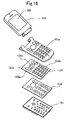
- FIGS. 15 - 17 One of the electronic apparatuses of such type is shown in FIGS. 15 - 17 as a mobile phone.
- this electronic apparatus 10 comprises a lower side body 101 including an operation input portion 102 and a voice input portion 103, an upper body 105 including an display panel 106 and a voice output portion 107, and a hinge portion 104 connecting the lower body 101 and the upper body 105 to be able to assume their fold-open and fold-closed positions.
- the lower side body 101 is constituted by an operational side chassis 101a and a backside chassis 101b. As shown in FIG.
- the electrically insulating sheet 123 is shown in FIG. 17 by a sectional view.
- the electrically insulating sheet 123 of embossed key and click type has a set of embossed key portions 123a respectively positioned below the key tops 122b.
- Each of the embossed key portions 123a is provided on its sphere concave side with a movable contact 126 made of metal spring material and having an arcuate section.
- the substrate 121 is provided on its upper side with stationary contacting parts 121a, 121b each facing to the movable contact 126.
- the substrate 121 is provided on its underside with a heat generating part 129 such as for example a known power amplifier or the like, while, each of the key tops 122b of the key sheet 122 is provided on its surface portion with a heat radiating layer, not shown clearly in the drawings, mainly made of aluminum and a decorative layer laminated on the surface of the heat radiating layer so as to facilitate heat radiation through the key top 122b.
- a heat radiating layer not shown clearly in the drawings, mainly made of aluminum and a decorative layer laminated on the surface of the heat radiating layer so as to facilitate heat radiation through the key top 122b.
- the electronic apparatus comprising the aforementioned push button switches, however, encounters the difficulties in increasing efficiency of heat soak of the chassis or body including the substrate 121 having the heat generating part 129 mounted thereon due to the fact that the respective heat radiating layers of the key tops 122b of the key sheet 122 are separate and independent from one another.
- the heat radiating layers are distant from the heat generating part 129 mounted on the substrate 121, and a certain number of layers having high thermal conductivity intervene between the heat radiating layers and the heat generating part 129. These also make it difficult to increase the efficiency of heat radiation through the heat radiating layers in order to decrease the temperature of the heat generating part 129 and other surrounding parts mounted in the vicinity of the heat generating part 129.
- the present invention has been made to solve such the drawbacks of the prior art. It is therefore an object of the present invention to provide an electronic apparatus capable of preventing the local heating of its chassis due to the high temperature rise of the heat generating part and other surrounding parts.
- the substrate can be efficiently heat soaked in every surface direction along the surface of the substrate by the heat conducting layer extending along the substrate.
- the heat conducting layer positioned in the vicinity of the surface of the substrate and extending along the surface of the substrate enables to broadly diffuse heat from a certain heat generating part on the substrate in the surface direction to increase efficiency of radiation of the heat.
- the heat conducting layer is a part or member forming part of the electrically insulating layer having thermal conductivity higher than that of the remaining part or member of the electrically insulating layer.
- the electrically insulating layer includes an insulating cover layer extending along the substrate and securely adhered onto the heat conducting layer. According to the present construction, if only the heat conducting layer is disposed within an area favorable for heat soak, the heat radiation becomes more effective and the heat conducting layer can be so laminated on the substrate as to be close to the substrate at the same time when the electrically insulating layer is attached to the substrate.
- the heat conducting layer may have an opening portion corresponding to the click portion of the electrically insulating layer. According to the present construction, the height of the click portion of the electrically insulating layer on the substrate can be reduced, and the push button switch can be reduced in volume and thickness and improved in click feeling.
- the inner edge of the opening portion of the heat conducting layer may be superimposed on the outer edge of the click portion of the electrically insulating layer or encircle the outer edge of the click portion of the electrically insulating layer.
- the electrically insulating layer have a white or glossy surface course.
- the white or glossy surface course of the electrically insulating layer can be an optical guide through which light emitted from a light source is guided to a certain illumination area. This enables to illuminate the illumination area with uniform intensity and color of the illumination.
- the electrically insulating layer may partly have a white or glossy portion as its surface course or may be formed in whole by white or glossy material.
- an electronic apparatus comprising any one of the aforementioned push button switches.
- the substrate with many electronic parts can be more efficiently heat soaked in an arbitrary direction along the surface of the substrate by the heat conducting layer extending along the substrate.
- the heat conducting layer positioned in the vicinity of the surface of the substrate and extending in a direction parallel to the surface of the substrate enables to broadly diffuse heat from the heat generating part and the like on the substrate in the surface direction of the substrate so as to increase efficiency of radiation of the heat. Consequently, it becomes possible to effectively suppress the temperature of the heat generating part and other surrounding parts and prevent the chassis of the electronic apparatus from being heated partly to high surface temperature.
- effect of heat soak of the substrate can be increased by sufficient heat radiation along the surface of the substrate through the heat conducting layer extending along the substrate.
- FIGS. 1-6 show a first embodiment of the electronic apparatus according to the present invention.
- the present embodiment is exemplified in a preferred electronic apparatus 1, as comprising a compact and thin type chassis 17 and a plurality of push button switches 10 each provided in the chassis 17 as shown in FIG. 3 .
- the electronic apparatus 1 in appearance has an exterior the same as or similar to that of the conventional mobile phone shown in FIG. 15 .
- the electronic apparatus 1 may be any one of other compact and thin portable/mobile electronic apparatuses such as for example a PDA (Personal Digital Assistant).
- each of the push button switches 10 comprises, on a printed circuit substrate 11, a first contacting part 11a and a second contacting part 11b operable to be brought into electrical conduction with the first contact 11a, and a flexible electrically insulating sheet 13 (i.e., an electrically insulating layer) covering the upper side surface of the printed circuit substrate 11.
- the electrically insulating sheet 13 has a click portion 13a in which the first contacting part 11 a and the second contacting part 11b are so disposed as to be brought into and out of electrical conduction therebetween in response to depression of the click portion 13a of the electrically insulating sheet 13.
- the click portion 13a is shaped into a projection portion having an approximately arcuate section and projecting from the flat sheet portion of the electrically insulating sheet 13 by a predetermined projection height toward the operational surface side of the electronic apparatus 1.
- the click portion 13a also has its approximately circular peripheral portion raised from the surface of the printed circuit substrate 11.
- the click portion 13a may not be projected or convexed on condition that the click portion 13a is out of operation (out of switch depression force).
- the click portion 13a may be flattened to be vertically in coincidence with the flat sheet portion of the electrically insulating sheet 13 under the state that the click portion 13a is out of operation (out of switch depression force).
- the flat click portion 13a may be depressed by the switch depression force to form a spherical concave portion so as to displace a movable contact provided on one side close to the printed circuit substrate 11 (i.e., inside of the click portion) toward the stationary contact, and resiliently return to its initial position with the click portion 13a when the switch depression force is released from the click portion 13a.
- the resilient return force of the click portion may be produced only by the electrically insulating sheet 13 or mainly produced by a conductive member forming the contact or other electrically conductive members engageable with the first and second contacting parts.
- the click portion of the electrically insulating sheet is therefore required only to be flexible to the degree sufficient to produce an elastic deformation and move the movable contact in response to the switch depression force.
- the peripheral portion of the click portion may be arbitrarily shaped in response to the shape of a depression member through which the switch depression force is transferred.
- the second contacting parts 11b on the printed circuit substrate 11 are separated from each other or collectively formed into an annular shape to have the first contact part 11 a put therebetween or therein in the direction along the surface of the printed circuit substrate 11 (right and left sides in FIG. 1 ; hereinafter referred to as "surface direction").
- These first and second contacting parts 11a and 11b are each electrically connected to an electronic control circuit, not shown in the drawing, provided on one side or/and the other side of the printed circuit substrate 11.
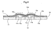
- the third contacting part 12 has a center portion 12c designed to function as a movable contact through which the first contact 11a and the second contact 11b can be brought into electrical conduction with each other when the third contacting part 12 is depressed by the switch depression force (i.e., the operational force for switching the push button switch) from one of the button portions 16a of the key sheet 16 through the corresponding click portion 13a of the electrically insulating sheet 13 and the center portion 12c is displaced to be close to the first contact 11a as shown in FIG. 4 .
- the switch depression force i.e., the operational force for switching the push button switch
- the undermost insulating layer 15a is composed of an electrically insulating resin material layer, e.g., a PET (polyethylene terephthalate) sheet and an adhesive or insulating adhesive layer not shown in the drawings.
- the undermost insulating layer 15b is composed of an electrically insulating resin material layer, e.g., a PET (polyethylene terephthalate) sheet.
- the insulating layers 15a, 15b are tacked to each other or united by adhesion or the like to form a tacked portion 15e, and cover and surround not only the lower and upper side surfaces of the heat conducting layer 14 but also the contour, i.e., the peripheral surface region 14e of the heat conducting layer 14.
- the peripheral edge portion of the electrically insulating sheet 13 is preferably covered and electrically insulated, but can be cut off to expose the peripheral surface region 14e of the heat conducting layer 14.
- One of the insulating layers 15a, 15b forming the insulating cover layer, e.g., the insulating layer 15b is larger in area than the heat conducting layer 14 and sufficient in area to cover the heat conducting layer 14.
- one of the insulating layers 15a, 15b may be the same in area as the other of the insulating layers 15a, 15b, e.g., the insulating layer 15a extending over the whole area of the electrically insulating sheet 13, or smaller in area than the insulating layer 15a.
- the heat conducting layer 14 is provided between the insulating layer 15a, i.e., the insulating retainer layer retaining the third contacting part 12 and securely adhered to the printed circuit substrate 11 and the insulating layer 15b, i.e., the insulating cover layer covering the heat conducting layer 14. And, the heat conducting layer 14 is on one side of the insulating layer 15a, i.e., the insulating retainer layer against the printed circuit substrate 11.
- the insulating layer 15a, the heat conducting layer 14 and the insulating layer 15b are laminated and securely integrally adhered to one another so as to collectively constitute the electrically insulating sheet 13, the undermost layer portion of which is securely mounted on the printed circuit substrate 11 by adhesion or the like.
- a plurality of light emitting elements such as for example a plurality of LEDs (Light Emitting Diodes) 18, while on the lower side of the printed circuit substrate 11 are mounted a heat generating part 19 such as a power amplifier or the like and many other electronic parts not shown in the drawing.
- the corresponding one of the engaging portions 16d just below the depressed button portion 16a downwardly moves one of the click portions 13a of the electrically insulating sheet 13 so as to depress the third contacting part 12 retained by the click portion 13a.
- the depressed third contacting part 12 is brought into deformation enough to bring the center portion 12c of the third contacting part 12 into contact with the first contact 11a as shown in FIG. 4 until the first contact 11a and the second contact 11b are electrically connected with each other through the third contacting part 12.
- the switching state of the push button switch 10 is changed from one to another/the other.
- the switching state is changed from the open and disconnected state to the closed and connected state at this time.
- the push button switch 10 is normal-open type, but can be changed to a normal close type.
- the switch depression force exerted on one of the button portions 16a of the key sheet 16 is released, and the corresponding one of the engaging portion 16d just below the depressed button portion 16a is upwardly moved by one of the click portion 13a of the electrically insulating sheet 13 as the click portion 13a of the electrically insulating sheet 13 and the third contacting part 12 return to their respective initial states and home positions.
- the third contacting part 12 brings its center portion 12c out of contact with the first contact 11a as shown in FIG. 2 and resiliently returns into the initial state to have an initial curvature and arcuate section until the first contact 11a and the second contact 11b are electrically disconnected from each other.
- the switching state of the push button switch 10 is changed back to one from another/the other. For example, the switching state is changed at this time to the open and disconnected state from the closed and connected state.
- the heat generating part 19 such as the power amplifier or the like on the printed circuit substrate 11 tends to generate heat by which the chassis 17 and the parts in the chassis 17 are raised in temperature around the heat generating part 19.
- the heat generated from the parts on the printed circuit substrate 11 is effectively transmitted in the surface direction (i.e., extending direction) of the heat conducting layer 14 through the heat conducting layer 14. Because of the existence of the heat conducting layer 14, the heat is diffused effectively in the surface direction of the printed circuit substrate 11, and the printed circuit substrate 11 including a large number of electronic parts is efficiently heat soaked.
- the heat generated from the heat generating part 19 is broadly diffused in the surface direction of the printed circuit substrate 11 by the reason that the heat conducting layer 14 extends along the printed circuit substrate 11 to be close to the printed circuit substrate 11. This makes it possible to increase efficiency of heat radiation from the heat generating part 19 and other surrounding parts. Consequently, it is possible to assuredly prevent the heat generating part 19 and other surrounding parts in the electronic apparatus 1 from being highly raised in temperature to the degree that the user feels partly uncomfortable in surface temperature of the chassis 17.
- the heat conducting layer 14 is made of a graphite sheet
- the graphite sheet can be thinned down to 100 micrometer thick or less. This enables to remarkably reduce the thickness of the electrically insulating sheet 13 and the thickness of the electronic apparatus 1.
- the thinned click portion 13a of the electrically insulating sheet 13 makes it possible to improve the click feeling during the switch depression operation by the main reason that the third contacting part 12 having elasticity and an arcuate section is adhered on the inside of the click portion 13a. It is therefore possible to produce a durable and tactile push button switch 10 superiorly improved in operational feeling (such as the click feeling).
- the electrically insulating sheet 13 includes the uppermost insulating layer 15b positioned on one side of the heat conducting layer 14 against the printed circuit substrate 11, and the undermost insulating layer 15a positioned on the other side of the heat conducting layer 14 with the printed circuit substrate 11. And, the undermost insulating layer 15a and the uppermost insulating layer 15b are tacked to each other or united so as to cover and surround the peripheral surface region 14e of the heat conducting layer 14. It is therefore possible to produce the highly heat-conductive electrically insulating sheet 13 having the heat conducting layer 14 inserted between the insulating layers 15a, 15b.
- the heat conducting layer 14 it is possible to automatically dispose the heat conducting layer 14 to be close to the printed circuit substrate 11 only by mounting the electrically insulating sheet 13 on the printed circuit substrate 11, since the electrically insulating sheet 13 is constituted by the insulating layers 15a, 15b each extending along the printed circuit substrate 11 and the heat conducting layer 14 securely adhered to at least one of the insulating layers 15a, 15b.
- the number of assembly processes of the present embodiment can therefore be reduced.
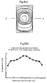
- FIGS. 5 in combination show a simulation result representative of the temperature distribution on the operational surface of the chassis 17 and calculated based on the positions of the heat generating part 19 and amount of heat generated from each of the heat generating part 19 and the like in the electronic apparatus 1 according to the present embodiment.
- FIG. 5(a) is explanatory view showing a temperature distribution image on the whole operational surface with a plurality of isothermal lines
- FIG. 5(b) is a graph showing a sectioned distribution profile of the surface temperature taken along a section line X-X in FIG. 5(a) .
- the chassis 17 has a thickness of 0.9 mm and a thermal conductivity of 0.3W/(m ⁇ k)
- the printed circuit substrate 11 has a thickness of 0.5 mm and a thermal conductivity of 35W/(m ⁇ k)
- the key sheet 16 has a thickness of 0.5 mm (corresponding to a height of 1 mm from the lower end of the support projection portion 16c) and a thermal conductivity of 0.2W/(m ⁇ k)
- the heat generating part 19 has a thickness of 1.0 mm and a thermal conductivity of 1W/(m ⁇ k)
- the electrically insulating sheet 13 including the graphite heat conducting layer 14 has a thickness of 0.1 mm and a thermal conductivity (in the surface direction) of 700W/(m ⁇ k).
- the electrically insulating sheet 13 covers the area within which the plurality of button portions 16a are arranged, but does not exceed over the whole area of the printed circuit substrate 11.
- the chassis 17 is efficiently heat soaked in the coverage of the electrically insulating sheet 13 using the graphite sheet, and the temperature of the operational surface of the chassis 17 lies within an approximately constant temperature range in the area where the button portions 16a are arranged.
- the graph in FIG. 5(b) indicates a tolerable temperature rise on the operational surface within the range of several degrees in comparison with the temperature on the periphery (i.e., both side ends of the graphed line in this figure) of the chassis 17 difficult to be affected by the heat generated in the chassis.
- FIGS. 6 in combination show another simulation result representing for comparison purpose the temperature distribution on the operational surface of the chassis of the electronic apparatus in which the heat conducting layer 14 is removed from the construction of the aforementioned embodiment.
- FIG. 6(a) is an explanatory view showing a temperature distribution image on the whole operational surface with a plurality of isothermal lines
- FIG. 6(b) is a graph showing a sectioned distribution profile of the surface temperature taken along a section line X-X in FIG. 6(a) .
- the surface temperature of the chassis becomes higher as the surface position nears the heat generating part 19 as shown in FIG. 6(a) . It is therefore apparent that the chassis is not efficiently heat soaked in the coverage of the electrically insulating sheet.
- the graph of FIG. 6(b) indicates an intolerable surface temperature rise at the position close to the heat generating part 19, and the temperature rise is approximately twice as large as the tolerable temperature rise of the aforementioned embodiment. It is apparent that the surface temperature of the chassis is partly remarkably raised in comparison with the temperature on the periphery (i.e., both side ends of the graphed line in this figure) of the chassis difficult to be affected by the heat generated in the chassis.
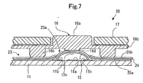
- FIGS. 7-9 show a second embodiment of the electronic apparatus according to the present invention.
- each of the push button switches 20 comprises, on the printed circuit substrate 11, the first contacting part 11a and the second contacting part 11b operable to be brought into electrical conduction with the first contact 11a, and a flexible electrically insulating sheet 23 (i.e., an electrically insulating layer) covering the upper side surface of the printed circuit substrate 11.
- the insulating sheet 23 has a click portion 23 a on the inside of which the first contacting part 11a and the second contacting part 11b are so disposed as to be brought into and out of electrical conduction therebetween in response to depression of the click portion 23a of the electrically insulating sheet 23.
- the printed circuit substrate 11 and the push button switches 20 are housed in the chassis 17 of the electronic apparatus 1. In the chassis 17 is additionally provided a key sheet 16.
- the second contacting parts 11b on the printed circuit substrate 11 are separated from each other or collectively formed into an annular shape to have the first contact part 11 a put therebetween or therein in the surface direction of the printed circuit substrate 11.
- the second contacting parts 11b positioned on both sides of the first contact 11a in FIG. 1 are held in contact with the third contacting part 12.
- the electrically insulating sheet 23 includes a heat conducting layer 24 and lower and upper insulating layers 25a, 25b (i.e., insulating cover layers) each extending along the printed circuit substrate 11.
- the heat conducting layer 24 has a thermal conductivity higher than those of the printed circuit substrate 11 and the insulating layers 25a, 25b of the electrically insulating sheet 23, and is for example constituted by a graphite sheet or a highly heat-conductive metal sheet.
- Each of the insulating layers 25a, 25b is composed of an electrically insulating resin material layer, e.g., a PET sheet.
- the undermost insulating layer 25a (i.e., lower insulating cover layer) of the electrically insulating sheet 23 forms an insulating retainer layer retaining the third contacting part 12 and securely adhered onto the printed circuit substrate 11, while on the other hand the uppermost insulating layer 25b (i.e., upper insulating cover layer) of the electrically insulating sheet 23 forms an insulating cover layer securely adhered onto the heat conducting layer 24 so as to cover the heat conducting layer 24.
- the electrically insulating sheet 23 may include an undermost insulating layer 25a formed with an opening corresponding to the click portion 23a in the same manner as the heat conducting layer 24. And, the opening inner edge 25e of the undermost insulating layer 25a may be overlapped with the opening inner edge 24e of the heat conducting layer 24. In this case, the uppermost insulating layer 25b of the electrically insulating sheet 23 forms an insulating retainer layer retaining the third contacting part 12 and fixedly connected to the printed circuit substrate 11 through the heat conducting layer 24 and the undermost insulating layer 25a.
- the undermost insulating layer 25a of the electrically insulating sheet 23 forms an insulating cover layer securely adhered onto the heat conducting layer 24 to cover and protect the heat conducting layer 24.
- the electrically insulating sheet 23 still has a thin portion singly composed of the insulating layer 25b within the area where the electrically insulating sheet 23 and the center portion 12c, i.e., the movable contact are overlapped, and that the click portion 23a of the electrically insulating sheet 23 is sufficiently flexible.
- the insulating layer 25a, the heat conducting layer 24 and the insulating layer 25b are laminated and securely integrally adhered to one another so as to collectively constitute the electrically insulating sheet 23, the undermost layer portion of which is securely mounted on the printed circuit substrate 11 by adhesion or the like.
- the undermost insulating layer 15a is composed of an electrically insulating resin material layer, e.g., a PET (polyethylene terephthalate) sheet and an adhesive or insulating adhesive layer not shown in the drawings.
- the third contacting part 12 is securely retained by the undermost insulating adhesive layer not shown in the drawings.
- the third contacting part 12 is positioned above or on the first and second contacting parts 11a, 11b of the printed circuit substrate 11 with the lower edge portion of the third contacting part 12 being held in contact with the second contact 11b on each side of the first contact 11a.
- either one of the insulating layers 25a, 25b and the heat conducting layer 24 are formed with their respective openings corresponding to the click portion 23a of the electrically insulating sheet 23.
- the electrically insulating sheet 23 has a thin portion singly composed of the insulating layer 25a or 25b within the area where the click portion 23a of the electrically insulating sheet 23 is held in contact with the engaging portion 16d of the key sheet 16. This enables to reduce the height of the click portion 23a on the printed circuit substrate 11 to practically reduce the size and thickness of the electronic apparatus 1. This also improves the click feeling of the button portions 16a by means of the flexible third contract 12 having plate spring feature.
- the click feeling means an operational feeling sensed by the user in the case that the reaction force from the button portion 16a is rapidly reduced when the stroke of the button portion 16a exceeds over a predetermined certain stroke to the degree that the user senses the stroke end of the button portion 16a.
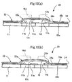
- FIG. 10 and FIG. 11 in combination show a third embodiment of the electronic apparatus according to the present invention.
- the electronic apparatus according to the present embodiment is a compact and thin portable electronic apparatus equipped with a plurality of push button switches 30 in the chassis in the same manner as in the aforementioned first embodiment.
- This electronic apparatus in appearance has an exterior the same as or similar to that of the conventional mobile phone shown in FIG. 15 .
- the constituent elements the same as those in the aforementioned first embodiment bear their respective reference numerals the same as those shown in FIGS. 1 to 4 , and are omitted in detailed description thereof.
- each of the push button switches 30 comprises, on the printed circuit substrate 11, the first contacting part 11a and the second contacting part 11b operable to be brought into electrical conduction with the first contact 11a, and a flexible electrically insulating sheet 33 (i.e., an electrically insulating layer) covering the upper side surface of the printed circuit substrate 11.
- the electrically insulating sheet 33 has a click portion 33a on the inside of which the first contacting part 11a and the second contacting part 11b are so disposed as to be brought into and out of electrical conduction therebetween in response to depression of the click portion 33a of the electrically insulating sheet 33.
- the printed circuit substrate 11 and the push button switch 30 are housed in the chassis 17 of the electronic apparatus 1 with a key sheet 16 additionally provided in the chassis 17.
- the electrically insulating sheet 33 includes a heat conducting layer 34 and lower and upper insulating layers 35a, 35b (i.e., insulating cover layers) each extending along the printed circuit substrate 11.
- the heat conducting layer 34 has a thermal conductivity higher than those of the printed circuit substrate 11 and the insulating layers 35a, 35b of the electrically insulating sheet 33, and is for example constituted by a graphite sheet or a highly heat-conductive metal sheet.
- Each of the insulating layers 35a, 35b is composed of an electrically insulating resin material layer, e.g., a PET sheet.
- the insulating layers 35a, 35b of the electrically insulating sheet 33 are disposed on both sides of the heat conducting layer 34 to oppose to each other, and securely adhered to each other around the periphery of the click portion 33a and within the opening inner edge 34e of the heat conducting layer 34.
- the third contacting part 12 is securely retained by at least one of the insulating layers 35a, 35b. For example, as shown in FIG.
- the lowermost insulating layer 35a (i.e., the lower insulating cover layer) of the electrically insulating sheet 33 forms an insulating retainer layer securely retaining the third contacting part 12 and securely adhered onto the printed circuit substrate 11, while on the other hand the uppermost insulating layer 35b (i.e., upper insulating cover layer) of the electrically insulating sheet 33 forms an insulating cover layer securely adhered onto the heat conducting layer 34 so as to cover the heat conducting layer 34.
- FIG. 10(b) shows a modified form of the push button switch 30, in which the uppermost insulating layer 35b of the electrically insulating sheet 33 forms an insulating retainer layer retaining the third contacting part 12 and fixedly connected to the printed circuit substrate 11 through the heat conducting layer 34 and the undermost insulating layer 35a.
- the undermost insulating layer 35a forms an insulating caver layer covering the lower side of the heat conducting layer 34 (i.e., the same side as the substrate).
- the electrically insulating sheet 33 has a thin portion thinner than the other portion thereof within the area where the electrically insulating sheet 33 and the center portion 12c, i.e., the movable contact are overlapped, and that the click portion 33a of the electrically insulating sheet 33 becomes sufficiently flexible.
- the electrically insulating sheet 33 has a thin portion within the area where the click portion 33a of the electrically insulating sheet 33 is held in contact with the engaging portion 16d of the key sheet 16. This enables to reduce the height of the click portion 33a on the printed circuit substrate 11 to practically reduce the size and thickness of the electronic apparatus 1. This also makes it possible to improve the click feeling of the button portions 16a by means of the flexible third contract 12 having plate spring feature.
- FIG. 12 and FIG. 13 in combination show a fourth embodiment of the electronic apparatus according to the present invention.
- each of the push button switches 40 comprises, on the printed circuit substrate 11, the first contacting part 11a and the second contacting part 11b operable to be brought into electrical conduction with the first contact 11a, and a flexible electrically insulating sheet 43 (i.e., an electrically insulating layer) covering the upper side surface of the printed circuit substrate 11.
- the electrically insulating sheet 43 has a click portion 43a on the inside of which the first contacting part 11a and the second contacting part 11b are so disposed as to be brought into and out of electrical conduction therebetween in response to depression of the click portion 43a of the electrically insulating sheet 43.
- the printed circuit substrate 11 and the push button switch 40 are housed in the chassis 17 of the electronic apparatus 1 with a key sheet 16 additionally provided in the chassis 17.
- the center portion 12c of the third contacting part 12 is adapted to function as a movable contact through which the first contact 11a and the second contact 11b can be brought into electrical conduction with each other when the third contacting part 12 is depressed by the switch depression force from one of the button portions 16a of the key sheet 16 through the corresponding click portion 43a of the electrically insulating sheet 43 and the center portion 12c is displaced onto the first contact 11a as shown in FIGS. 13(a) and 13(b) .
- the center portion 12c of the third contacting part 12 is further brought out of contact and electrical conduction with the first contact 11a and resiliently returns to the home position distant from the first contact 11a as shown in FIGS. 12(a) and 12(b) when the switch depression force from one of the button portions 16a of the key sheet 16 is released.
- the uppermost insulating layer 45b of the electrically insulating sheet 43 forms an insulating retainer layer retaining the third contacting part 12 and fixedly connected to the printed circuit substrate 11 through the heat conducting layer 44 and the undermost insulating layer 45a, while, on the other hand, the heat conducting layer 44 and the undermost insulating layer 45a of the electrically insulating sheet 43 have their respective opening portions within the area over which the switch depression force from the engaging portion 16d may be exerted.
- the insulating layers 45a, 45b and the heat conducting layer 44 are laminated and securely integrally adhered to one another so as to collectively constitute the electrically insulating sheet 43, the undermost layer portion of which is securely mounted on the printed circuit substrate 11 by adhesion or the like.
- the third contacting part 12 is securely retained by the undermost insulating adhesive layer not shown in the drawings, and the third contacting part 12 is positioned above or on the first and second contacting parts 11a, 11b of the printed circuit substrate 11 with the lower edge portion of the third contacting part 12 being held in contact with the second contact 11b on each side of the first contact 11a.
- each of the push button switches 50 comprises, on a printed circuit substrate 51, a first contacting part 51a and a second contacting part 51b operable to be brought into electrical conduction with the first contacting part 51a, and a flexible electrically insulating sheet 53 (i.e., an electrically insulating layer) covering the upper side surface of the printed circuit substrate 51.
- the electrically insulating sheet 53 has a click portion 53a in which the first contacting part 51a and the second contacting part 51b are so disposed as to be brought into and out of electrical conduction therebetween in response to depression of the click portion 53a of the electrically insulating sheet 53.
- the printed circuit substrate 51 and the push button switch 50 are housed in the chassis 17 of the electronic apparatus 1 with the key sheet 16 additionally provided in the chassis 17.
- the key sheet 16 is equipped with a plurality of button portions 16a (i.e., depression member) each operable to depress the click portion 53a of the electrically insulating sheet 53 and a flexible viscoelastic, e.g., rubber elastic sheet 16b on which the button portions 16a are mounted.
- the rubber elastic sheet 16b is provided and integrally formed on its underside with a plurality of support projection portion 16c projecting toward the electrically insulating sheet 53 and a plurality of engaging portions 16d (i.e., depression member) each engageable to the click portion 53a of the electrically insulating sheet 53.
- the center portion 12c of the third contacting part 12 is brought out of contact and electrical conduction with the first contact 51a, and resiliently returns to the home position distant from the first contact 51a.
- the electrically insulating sheet 53 includes a heat conducting layer 54 and lower and upper insulating layers 55a, 55b (i.e., insulating cover layers) each extending along the printed circuit substrate 51.
- the heat conducting layer 54 has a thermal conductivity higher than those of the printed circuit substrate 51 and the insulating layers 55a, 55b of the electrically insulating sheet 53, and is for example constituted by a graphite sheet or a highly heat-conductive metal sheet or the like.
- Each of the insulating layers 55a, 55b is composed of an electrically insulating resin material layer, e.g., a PET sheet.
- the undermost insulating layer 55a (i.e., the lower insulating cover layer) of the electrically insulating sheet 53 forms an insulating retainer layer retaining the third contacting part 12 and securely adhered onto the printed circuit substrate 51, while, on the other hand, the uppermost insulating layer 55b (i.e., the upper insulating cover layer) of the electrically insulating sheet 53 forms an insulating cover layer securely adhered onto the heat conducting layer 54 so as to cover and protect the heat conducting layer 54.
- the insulating layer 55a, the heat conducting layer 54 and the insulating layer 55b are laminated and securely integrally adhered to one another so as to collectively constitute the electrically insulating sheet 53, the undermost layer portion of which is securely mounted on the printed circuit substrate 51 by adhesion or the like.
- the third contacting part 12 on the inside of the click portion 53a of the electrically insulating sheet 53 is positioned and retained by the click portion 53a to be above or on the first and second contacting parts 51a, 51b with the lower edge portion of the third contacting part 12 being held in contact with the second contact 51b on each side of the first contact 51a.
- the heat conducting layer 54 has electrical conductivity and electrically connected through an electrical connection layer 58, made of an electrically conductive adhesive layer or the like, with a ground pattern 51c that is an electrically conductive land portion provided on the printed circuit substrate 51.
- an electrical connection layer 58 made of an electrically conductive adhesive layer or the like
- a ground pattern 51c that is an electrically conductive land portion provided on the printed circuit substrate 51.
Landscapes
- Push-Button Switches (AREA)
Applications Claiming Priority (2)
| Application Number | Priority Date | Filing Date | Title |
|---|---|---|---|
| PCT/JP2005/023881 WO2007074512A1 (fr) | 2005-12-27 | 2005-12-27 | Interrupteur à bouton-poussoir |
| PCT/JP2006/311309 WO2007074547A1 (fr) | 2005-12-27 | 2006-06-06 | Interrupteur à bouton-poussoir et appareil électronique équipé de celui-ci |
Publications (2)
| Publication Number | Publication Date |
|---|---|
| EP1968085A1 true EP1968085A1 (fr) | 2008-09-10 |
| EP1968085A4 EP1968085A4 (fr) | 2009-06-17 |
Family
ID=38217749
Family Applications (1)
| Application Number | Title | Priority Date | Filing Date |
|---|---|---|---|
| EP06757049A Withdrawn EP1968085A4 (fr) | 2005-12-27 | 2006-06-06 | Interrupteur à bouton-poussoir et appareil électronique équipé de celui-ci |
Country Status (5)
| Country | Link |
|---|---|
| US (1) | US8071902B2 (fr) |
| EP (1) | EP1968085A4 (fr) |
| JP (1) | JPWO2007074512A1 (fr) |
| CN (1) | CN101346791A (fr) |
| WO (2) | WO2007074512A1 (fr) |
Families Citing this family (10)
| Publication number | Priority date | Publication date | Assignee | Title |
|---|---|---|---|---|
| US7978467B2 (en) * | 2007-02-05 | 2011-07-12 | Panasonic Corporation | Key sheet, press switch and electronic device provided with the press switch |
| US8111522B2 (en) * | 2008-04-29 | 2012-02-07 | Apple Inc. | Switch structures for use on printed circuit boards |
| US20110049391A1 (en) * | 2009-09-01 | 2011-03-03 | Cheng-Pu Yang | Storage Container Having Sterilizing Function by Using Ultraviolet Rays |
| US8362371B2 (en) * | 2009-09-28 | 2013-01-29 | Research In Motion Limited | Key assembly for an electronic device having one-piece keycaps and multi-touch preventing supports |
| US8274005B2 (en) * | 2010-02-26 | 2012-09-25 | Research In Motion Limited | Keypad assembly |
| US8502097B2 (en) | 2010-12-22 | 2013-08-06 | Research In Motion Limited | Bridge style push-button with anchoring |
| USD698324S1 (en) * | 2012-01-19 | 2014-01-28 | Samsung Electronics Co., Ltd. | TV receiver |
| US20150129406A1 (en) * | 2013-11-13 | 2015-05-14 | Changshu Sunrex Technology Co., Ltd. | Keyboard device |
| CN107957760A (zh) * | 2017-11-20 | 2018-04-24 | 安徽省未来博学信息技术有限公司 | 电子设备耐高温主板 |
| EP4228451B1 (fr) * | 2020-10-16 | 2025-08-27 | JT International SA | Dispositif de génération d'aérosol doté d'un couvercle flexible |
Family Cites Families (14)
| Publication number | Priority date | Publication date | Assignee | Title |
|---|---|---|---|---|
| JPS6387730A (ja) * | 1986-09-30 | 1988-04-19 | Nec Corp | 電子部品の実装構造 |
| JPS6387730U (fr) * | 1986-11-28 | 1988-06-08 | ||
| JPH0589743A (ja) * | 1991-05-13 | 1993-04-09 | Tokyo Shimoda Kogyo Kk | 照光式メンブレンスイツチ |
| JPH11232963A (ja) * | 1998-02-13 | 1999-08-27 | Matsushita Electric Ind Co Ltd | パネルスイッチ用可動接点体およびそれを用いたパネルスイッチ |
| JP2000311050A (ja) * | 1999-04-28 | 2000-11-07 | Matsushita Electric Ind Co Ltd | キーボード装置 |
| JP3938846B2 (ja) * | 2000-03-16 | 2007-06-27 | アルプス電気株式会社 | 板バネ付シート、及びこの板バネ付シートを用いたスイッチ装置 |
| JP4101586B2 (ja) * | 2002-08-19 | 2008-06-18 | セイコープレシジョン株式会社 | 照光スイッチ |
| JP4102696B2 (ja) * | 2003-04-10 | 2008-06-18 | 埼玉日本電気株式会社 | 電子機器の入力装置の放熱構造及び該構造を備えてなる携帯電話機器 |
| JP2004310965A (ja) * | 2003-04-10 | 2004-11-04 | Sony Corp | ディスクドライブ装置 |
| JP3808073B2 (ja) * | 2003-12-05 | 2006-08-09 | シチズン電子株式会社 | キーシートモジュール |
| JP2005332432A (ja) * | 2004-05-18 | 2005-12-02 | Matsushita Electric Ind Co Ltd | 光ピックアップ及び光ディスク装置 |
| JP4801537B2 (ja) * | 2005-10-13 | 2011-10-26 | ポリマテック株式会社 | キーシート |
| JP4843419B2 (ja) * | 2005-10-13 | 2011-12-21 | ポリマテック株式会社 | キーシート |
| US7978467B2 (en) * | 2007-02-05 | 2011-07-12 | Panasonic Corporation | Key sheet, press switch and electronic device provided with the press switch |
-
2005
- 2005-12-27 JP JP2007551826A patent/JPWO2007074512A1/ja active Pending
- 2005-12-27 WO PCT/JP2005/023881 patent/WO2007074512A1/fr not_active Ceased
-
2006
- 2006-06-06 WO PCT/JP2006/311309 patent/WO2007074547A1/fr not_active Ceased
- 2006-06-06 US US12/158,163 patent/US8071902B2/en not_active Expired - Fee Related
- 2006-06-06 CN CNA2006800490377A patent/CN101346791A/zh active Pending
- 2006-06-06 EP EP06757049A patent/EP1968085A4/fr not_active Withdrawn
Also Published As
| Publication number | Publication date |
|---|---|
| WO2007074512A1 (fr) | 2007-07-05 |
| US8071902B2 (en) | 2011-12-06 |
| WO2007074547A1 (fr) | 2007-07-05 |
| JPWO2007074512A1 (ja) | 2009-06-04 |
| US20090090607A1 (en) | 2009-04-09 |
| CN101346791A (zh) | 2009-01-14 |
| EP1968085A4 (fr) | 2009-06-17 |
Similar Documents
| Publication | Publication Date | Title |
|---|---|---|
| KR100988099B1 (ko) | 도광 시트 및 이것을 이용한 가동 접점체와 스위치 | |
| US7978467B2 (en) | Key sheet, press switch and electronic device provided with the press switch | |
| US9029723B2 (en) | Keypad apparatus and methods | |
| US7705259B2 (en) | Thin key sheet and thin key unit incorporating the thin key sheet | |
| EP3021199B1 (fr) | Clavier à étui cuir et commutateur tactile | |
| US7465889B2 (en) | Pushbutton switch cover sheet and method of manufacturing the same | |
| EP1968085A1 (fr) | Interrupteur à bouton-poussoir et appareil électronique équipé de celui-ci | |
| US9142370B2 (en) | Illuminated keyboard | |
| JP2007523456A (ja) | スイッチ | |
| US10020139B2 (en) | Key structure | |
| JP2009026729A (ja) | 導光機能付き可動接点体とそれを用いた入力装置 | |
| JP5136934B2 (ja) | フレキシブルプリント配線板、入力モジュール及び携帯機器 | |
| EP2472544B1 (fr) | Appareil de clavier et procédé de fabrication | |
| JP2010034008A (ja) | 導光シートスイッチユニット | |
| JP2003303530A (ja) | ドームスイッチ | |
| US20180143698A1 (en) | Keyboard | |
| JP4801676B2 (ja) | 押圧式スイッチ及びこれを備えた電子機器 | |
| JP7658070B2 (ja) | シートキー及び電子機器 | |
| JP2004247160A (ja) | 押釦スイッチ用部材 | |
| JP5619369B2 (ja) | シートスイッチ | |
| JP2010192275A (ja) | 導光シートスイッチ | |
| JP2023078491A (ja) | プッシュスイッチ | |
| JP2002117743A (ja) | 自照式シート部材 | |
| WO2008078143A1 (fr) | Ensemble clavier | |
| JP2023078492A (ja) | プッシュスイッチ |
Legal Events
| Date | Code | Title | Description |
|---|---|---|---|
| PUAI | Public reference made under article 153(3) epc to a published international application that has entered the european phase |
Free format text: ORIGINAL CODE: 0009012 |
|
| 17P | Request for examination filed |
Effective date: 20080530 |
|
| AK | Designated contracting states |
Kind code of ref document: A1 Designated state(s): DE FR GB |
|
| RAP1 | Party data changed (applicant data changed or rights of an application transferred) |
Owner name: PANASONIC CORPORATION |
|
| RBV | Designated contracting states (corrected) |
Designated state(s): DE FR GB |
|
| A4 | Supplementary search report drawn up and despatched |
Effective date: 20090520 |
|
| RIC1 | Information provided on ipc code assigned before grant |
Ipc: H01H 13/70 20060101ALI20090514BHEP Ipc: H01H 13/704 20060101ALI20090514BHEP Ipc: H01H 13/04 20060101AFI20070821BHEP |
|
| 17Q | First examination report despatched |
Effective date: 20090831 |
|
| DAX | Request for extension of the european patent (deleted) | ||
| STAA | Information on the status of an ep patent application or granted ep patent |
Free format text: STATUS: THE APPLICATION IS DEEMED TO BE WITHDRAWN |
|
| 18D | Application deemed to be withdrawn |
Effective date: 20130103 |