EP1969691B1 - Detecteur de charge pour un gradateur - Google Patents
Detecteur de charge pour un gradateur Download PDFInfo
- Publication number
- EP1969691B1 EP1969691B1 EP06828000A EP06828000A EP1969691B1 EP 1969691 B1 EP1969691 B1 EP 1969691B1 EP 06828000 A EP06828000 A EP 06828000A EP 06828000 A EP06828000 A EP 06828000A EP 1969691 B1 EP1969691 B1 EP 1969691B1
- Authority
- EP
- European Patent Office
- Prior art keywords
- signal
- voltage
- circuit
- ringing
- load
- Prior art date
- Legal status (The legal status is an assumption and is not a legal conclusion. Google has not performed a legal analysis and makes no representation as to the accuracy of the status listed.)
- Not-in-force
Links
- 230000001939 inductive effect Effects 0.000 claims abstract description 51
- 238000001514 detection method Methods 0.000 claims abstract description 21
- 238000000034 method Methods 0.000 claims description 24
- 230000008859 change Effects 0.000 claims description 10
- 230000000694 effects Effects 0.000 claims description 4
- 238000001914 filtration Methods 0.000 claims description 2
- 230000006870 function Effects 0.000 description 17
- 239000003990 capacitor Substances 0.000 description 11
- 230000007704 transition Effects 0.000 description 10
- 238000012421 spiking Methods 0.000 description 9
- 238000010586 diagram Methods 0.000 description 5
- 230000005611 electricity Effects 0.000 description 4
- 230000000630 rising effect Effects 0.000 description 4
- 230000004913 activation Effects 0.000 description 3
- 238000005516 engineering process Methods 0.000 description 3
- 230000004044 response Effects 0.000 description 3
- XEEYBQQBJWHFJM-UHFFFAOYSA-N Iron Chemical group [Fe] XEEYBQQBJWHFJM-UHFFFAOYSA-N 0.000 description 2
- 230000000903 blocking effect Effects 0.000 description 2
- 230000008878 coupling Effects 0.000 description 2
- 238000010168 coupling process Methods 0.000 description 2
- 238000005859 coupling reaction Methods 0.000 description 2
- 230000010355 oscillation Effects 0.000 description 2
- 230000001960 triggered effect Effects 0.000 description 2
- 230000009471 action Effects 0.000 description 1
- 230000003044 adaptive effect Effects 0.000 description 1
- 230000006399 behavior Effects 0.000 description 1
- 238000010276 construction Methods 0.000 description 1
- 238000009795 derivation Methods 0.000 description 1
- 230000005669 field effect Effects 0.000 description 1
- 230000001976 improved effect Effects 0.000 description 1
- 238000009434 installation Methods 0.000 description 1
- 238000004519 manufacturing process Methods 0.000 description 1
- 230000007246 mechanism Effects 0.000 description 1
- 229910044991 metal oxide Inorganic materials 0.000 description 1
- 150000004706 metal oxides Chemical class 0.000 description 1
- 230000004048 modification Effects 0.000 description 1
- 238000012986 modification Methods 0.000 description 1
- 229910052754 neon Inorganic materials 0.000 description 1
- GKAOGPIIYCISHV-UHFFFAOYSA-N neon atom Chemical compound [Ne] GKAOGPIIYCISHV-UHFFFAOYSA-N 0.000 description 1
- 230000003071 parasitic effect Effects 0.000 description 1
- 230000008569 process Effects 0.000 description 1
- 230000000717 retained effect Effects 0.000 description 1
- 239000004065 semiconductor Substances 0.000 description 1
Images
Classifications
-
- H—ELECTRICITY
- H05—ELECTRIC TECHNIQUES NOT OTHERWISE PROVIDED FOR
- H05B—ELECTRIC HEATING; ELECTRIC LIGHT SOURCES NOT OTHERWISE PROVIDED FOR; CIRCUIT ARRANGEMENTS FOR ELECTRIC LIGHT SOURCES, IN GENERAL
- H05B39/00—Circuit arrangements or apparatus for operating incandescent light sources
- H05B39/04—Controlling
- H05B39/041—Controlling the light-intensity of the source
- H05B39/044—Controlling the light-intensity of the source continuously
- H05B39/048—Controlling the light-intensity of the source continuously with reverse phase control
-
- H—ELECTRICITY
- H02—GENERATION; CONVERSION OR DISTRIBUTION OF ELECTRIC POWER
- H02M—APPARATUS FOR CONVERSION BETWEEN AC AND AC, BETWEEN AC AND DC, OR BETWEEN DC AND DC, AND FOR USE WITH MAINS OR SIMILAR POWER SUPPLY SYSTEMS; CONVERSION OF DC OR AC INPUT POWER INTO SURGE OUTPUT POWER; CONTROL OR REGULATION THEREOF
- H02M5/00—Conversion of AC power input into AC power output, e.g. for change of voltage, for change of frequency, for change of number of phases
- H02M5/02—Conversion of AC power input into AC power output, e.g. for change of voltage, for change of frequency, for change of number of phases without intermediate conversion into DC
- H02M5/04—Conversion of AC power input into AC power output, e.g. for change of voltage, for change of frequency, for change of number of phases without intermediate conversion into DC by static converters
- H02M5/22—Conversion of AC power input into AC power output, e.g. for change of voltage, for change of frequency, for change of number of phases without intermediate conversion into DC by static converters using discharge tubes with control electrode or semiconductor devices with control electrode
- H02M5/275—Conversion of AC power input into AC power output, e.g. for change of voltage, for change of frequency, for change of number of phases without intermediate conversion into DC by static converters using discharge tubes with control electrode or semiconductor devices with control electrode using devices of a triode or transistor type requiring continuous application of a control signal
- H02M5/293—Conversion of AC power input into AC power output, e.g. for change of voltage, for change of frequency, for change of number of phases without intermediate conversion into DC by static converters using discharge tubes with control electrode or semiconductor devices with control electrode using devices of a triode or transistor type requiring continuous application of a control signal using semiconductor devices only
-
- H—ELECTRICITY
- H03—ELECTRONIC CIRCUITRY
- H03K—PULSE TECHNIQUE
- H03K17/00—Electronic switching or gating, i.e. not by contact-making and –breaking
- H03K17/08—Modifications for protecting switching circuit against overcurrent or overvoltage
- H03K17/082—Modifications for protecting switching circuit against overcurrent or overvoltage by feedback from the output to the control circuit
- H03K17/0822—Modifications for protecting switching circuit against overcurrent or overvoltage by feedback from the output to the control circuit in field-effect transistor switches
-
- H—ELECTRICITY
- H03—ELECTRONIC CIRCUITRY
- H03K—PULSE TECHNIQUE
- H03K17/00—Electronic switching or gating, i.e. not by contact-making and –breaking
- H03K17/16—Modifications for eliminating interference voltages or currents
- H03K17/161—Modifications for eliminating interference voltages or currents in field-effect transistor switches
- H03K17/165—Modifications for eliminating interference voltages or currents in field-effect transistor switches by feedback from the output circuit to the control circuit
-
- Y—GENERAL TAGGING OF NEW TECHNOLOGICAL DEVELOPMENTS; GENERAL TAGGING OF CROSS-SECTIONAL TECHNOLOGIES SPANNING OVER SEVERAL SECTIONS OF THE IPC; TECHNICAL SUBJECTS COVERED BY FORMER USPC CROSS-REFERENCE ART COLLECTIONS [XRACs] AND DIGESTS
- Y02—TECHNOLOGIES OR APPLICATIONS FOR MITIGATION OR ADAPTATION AGAINST CLIMATE CHANGE
- Y02B—CLIMATE CHANGE MITIGATION TECHNOLOGIES RELATED TO BUILDINGS, e.g. HOUSING, HOUSE APPLIANCES OR RELATED END-USER APPLICATIONS
- Y02B20/00—Energy efficient lighting technologies, e.g. halogen lamps or gas discharge lamps
Definitions
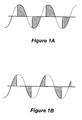
- the dimmer circuit In trailing edge technology, the dimmer circuit "chops out “or blocks conduction of electricity by the load in the back part of each half cycle.
- the method further comprises only detecting the peak value of the voltage ringing signal during a brief period at each half cycle of the voltage signal applied to the load so as to minimise the effect of electrical noise.
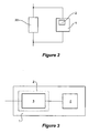
- load type detector 2 is provided by an inductive load detector 3, as shown in Figure 3 .
- universal dimmer 1 also has a mode control circuit 4, for changing the mode of operation of universal dimmer 1.
- mode control circuit 4 changes the operating mode of universal dimmer 1 from trailing edge to leading edge, as is known to the person skilled in the art.
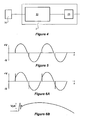
- Figure 6A now depicts the voltage across the dimmer at start-up at low conduction angle in trailing edge mode, when the dimmer 1 is connected to an inductive load.
- the dimmer voltage rises from near zero volts to momentarily exceed the instantaneous line voltage.
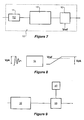
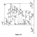
- resistors R18, R19 & R20 are selected to ensure that Q7 conduction status follows that of Q6, while Q8 assumes the opposite conduction status.
- Q7 provides a level shifting function, while Q8 provides an inversion function.
- Filter input resistor R2 provides high frequency "noise" rejection function.
- Output resistor R3, in conjunction with existing latch circuit input resistor R5 and transistor Q2, are used to form a rudimentary comparator function to determine the required detector output voltage level to trigger the latch.
Landscapes
- Engineering & Computer Science (AREA)
- Power Engineering (AREA)
- Circuit Arrangement For Electric Light Sources In General (AREA)
- Dc-Dc Converters (AREA)
Abstract
Claims (15)
- Circuit (3) pour détecter la présence d'une charge inductive (30), caractérisé en ce que ce circuit comprend :un détecteur d'ondulation de tension (10) pour détecter un signal d'ondulation de tension de part et d'autre de la charge inductive (30) comprenant :un filtre (11) pour extraire le signal d'ondulation de tension, ce filtre éliminant par filtrage une fréquence de tension secteur dans une forme d'onde de part et d'autre de la charge inductive ; etun détecteur de crêtes (12) pour détecter des crêtes dans le signal d'ondulation de tension ; etun générateur de signal pour générer un signal indiquant la présence de la charge inductive (30) lors de la détection par le détecteur d'ondulation de tension (10) dudit signal d'ondulation de tension.
- Circuit selon la revendication 1, dans lequel le filtre (11) est un filtre passe-haut.
- Circuit selon la revendication 1 ou 2, dans lequel le détecteur de crêtes (12) détecte l'amplitude d'ondulation des crêtes dans le signal d'ondulation de tension et génère un signal c.c. correspondant à l'amplitude d'ondulation détectée.
- Circuit selon la revendication 3, comprenant en outre un accumulateur c.c. pour accumuler le signal c.c. dans le temps afin de fournir un signal c.c. accumulé.
- Circuit selon la revendication 4, comprenant en outre un comparateur (13) pour comparer le signal c.c. accumulé avec une tension de référence et pour produire une sortie lorsque le signal c.c. accumulé dépasse la tension de référence.
- Circuit selon la revendication 5, comprenant en outre un indicateur de charge inductive pour générer un signal indiquant la présence de la charge inductive (30) lorsque la sortie du comparateur indique que le signal c.c. accumulé dépasse la tension de référence.
- Circuit selon l'une quelconque des revendications 1 à 6, comprenant en outre un générateur de signal pour générer un signal à un circuit de changement de mode pour changer un mode de fonctionnement d'un circuit gradateur d'un fonctionnement dans le mode flanc arrière à un fonctionnement dans le mode flanc avant lors de la détection du signal d'ondulation de tension.
- Circuit gradateur comprenant le circuit selon l'une quelconque des revendications 1 à 7.
- Procédé pour détecter la présence d'une charge inductive, caractérisé en ce que ce procédé comprend :la détection d'un signal d'ondulation de tension de part et d'autre de la charge, cette détection du signal d'ondulation de tension comprenant :le filtrage de la forme d'onde de part et d'autre de la charge inductive en utilisant un filtre haute fréquence pour éliminer par filtrage une fréquence de tension secteur et extraire le signal d'ondulation de tension ; etla détection de crêtes dans le signal d'ondulation de tension ; etla génération d'un signal indiquant la présence de la charge inductive lors de la détection dudit signal d'ondulation de tension.
- Procédé selon la revendication 9, comprenant en outre la détection de l'amplitude d'ondulation des crêtes dans le signal d'ondulation de tension et la génération d'un signal c.c. correspondant à l'amplitude d'ondulation détectée.
- Procédé selon la revendication 10, comprenant en outre la détection de l'amplitude d'ondulation des crêtes dans le signal d'ondulation de tension seulement pendant une brève période à chaque demi-cycle du signal de tension appliqué sur la charge afin de réduire au minimum l'effet du bruit électrique.
- Procédé selon l'une quelconque des revendications 10 ou 11, comprenant en outre l'accumulation du signal c.c. dans le temps pour fournir un signal c.c. accumulé.
- Procédé selon la revendication 12, comprenant en outre la comparaison du signal c.c. accumulé avec une tension de référence et la génération d'une sortie lorsque le signal c.c. accumulé dépasse la tension de référence.
- Procédé selon la revendication 13, dans lequel la sortie est un signal indiquant la présence de la charge inductive.
- Procédé selon l'une quelconque des revendications 9 à 14, comprenant en outre un signal pour changer un mode de fonctionnement d'un circuit gradateur d'un fonctionnement dans le mode flanc arrière à un fonctionnement dans le mode flanc avant lors de la détection du signal d'ondulation de tension.
Applications Claiming Priority (3)
| Application Number | Priority Date | Filing Date | Title |
|---|---|---|---|
| AU2005906949A AU2005906949A0 (en) | 2005-12-12 | Load detector for a dimmer | |
| AU2005906990A AU2005906990A0 (en) | 2005-12-12 | A universal dimmer | |
| PCT/AU2006/001882 WO2007068041A1 (fr) | 2005-12-12 | 2006-12-12 | Detecteur de charge pour un gradateur |
Publications (3)
| Publication Number | Publication Date |
|---|---|
| EP1969691A1 EP1969691A1 (fr) | 2008-09-17 |
| EP1969691A4 EP1969691A4 (fr) | 2010-03-03 |
| EP1969691B1 true EP1969691B1 (fr) | 2012-06-27 |
Family
ID=38162470
Family Applications (2)
| Application Number | Title | Priority Date | Filing Date |
|---|---|---|---|
| EP06817612A Not-in-force EP1961278B1 (fr) | 2005-12-12 | 2006-12-12 | Gradateur universel |
| EP06828000A Not-in-force EP1969691B1 (fr) | 2005-12-12 | 2006-12-12 | Detecteur de charge pour un gradateur |
Family Applications Before (1)
| Application Number | Title | Priority Date | Filing Date |
|---|---|---|---|
| EP06817612A Not-in-force EP1961278B1 (fr) | 2005-12-12 | 2006-12-12 | Gradateur universel |
Country Status (8)
| Country | Link |
|---|---|
| US (2) | US8085160B2 (fr) |
| EP (2) | EP1961278B1 (fr) |
| AU (1) | AU2006324377B2 (fr) |
| DK (2) | DK1961278T3 (fr) |
| MY (2) | MY163668A (fr) |
| NZ (2) | NZ568937A (fr) |
| TW (2) | TW200738068A (fr) |
| WO (2) | WO2007068040A1 (fr) |
Families Citing this family (24)
| Publication number | Priority date | Publication date | Assignee | Title |
|---|---|---|---|---|
| US20080246414A1 (en) * | 2007-04-05 | 2008-10-09 | Jian Xu | Inductive load sensor for dimmer circuit |
| EP2015616B1 (fr) | 2007-07-13 | 2010-09-08 | AB Plast S.r.l. | Procédé de reconnaissance de charge pour variateur et dispositif pour la mise en oeuvre de ce procédé |
| AU2008301235B2 (en) | 2007-09-19 | 2012-11-15 | Clipsal Australia Pty Ltd | Dimmer circuit with overcurrent detection |
| JP5444343B2 (ja) | 2008-07-17 | 2014-03-19 | アイシス イノヴェイション リミテッド | ユーティリティ計測器 |
| US8222832B2 (en) | 2009-07-14 | 2012-07-17 | Iwatt Inc. | Adaptive dimmer detection and control for LED lamp |
| US8698408B2 (en) * | 2009-11-25 | 2014-04-15 | Lutron Electronics Co., Inc. | Two-wire dimmer switch for low-power loads |
| WO2012168828A2 (fr) | 2011-06-10 | 2012-12-13 | Koninklijke Philips Electronics N.V. | Source de lumière led |
| EP2600698B1 (fr) * | 2011-11-30 | 2016-01-20 | Hager Controls SAS | Dispositif variateur de l'intensité de la lumière dans des charges lumineuses |
| WO2013148221A1 (fr) | 2012-03-28 | 2013-10-03 | Lutron Electronics Co., Inc. | Procédé et appareil de réglage de phase d'une charge |
| US9084324B2 (en) | 2013-02-26 | 2015-07-14 | Lutron Electronics Co., Inc. | Load control device having automatic setup for controlling capacitive and inductive loads |
| CN104035348B (zh) * | 2014-05-29 | 2017-01-04 | 东莞高仪电子科技有限公司 | 数位万用型调光器 |
| DE102015214633B3 (de) * | 2015-07-31 | 2016-09-22 | Siemens Schweiz Ag | Dimmvorrichtung und Verfahren zur Leistungssteuerung einer wechselstrombetriebenen Beleuchtungsvorrichtung |
| DE102015214631B3 (de) * | 2015-07-31 | 2016-11-03 | Siemens Schweiz Ag | Dimmvorrichtung und Verfahren zur Leistungssteuerung einer Leuchteinrichtung |
| US10231297B2 (en) | 2015-11-24 | 2019-03-12 | Philips Lighting Holding B.V. | Lighting apparatus control switch and method |
| FR3045270B1 (fr) * | 2015-12-14 | 2019-11-22 | Delta Dore | Procede et dispositif de gestion du fonctionnement d'un dispositif d'eclairage. |
| US10845397B2 (en) * | 2017-01-30 | 2020-11-24 | Wirepath Home Systems, Llc | Systems and methods for detecting load coupling and for detecting a load type |
| US9992849B1 (en) | 2017-08-15 | 2018-06-05 | Crestron Electronics, Inc. | Overvoltage detection in a dimmer |
| US10080273B1 (en) | 2017-11-14 | 2018-09-18 | Crestron Electronics, Inc. | Automatic load detection in a dimmer |
| US10517164B1 (en) | 2019-05-09 | 2019-12-24 | RAB Lighting Inc. | Universal phase control dimmer for wireless lighting control |
| US11664741B2 (en) | 2019-07-25 | 2023-05-30 | Susan Rhodes | System and method for AC power control |
| CN110531283B (zh) * | 2019-09-10 | 2021-10-22 | 温州力沃电器有限公司 | 一种调光开关的负载检测方法 |
| US11470697B2 (en) * | 2020-09-15 | 2022-10-11 | Boca Flasher, Inc. | Autosensing dimmer for light-emitting diodes |
| CN112684238B (zh) * | 2021-01-08 | 2024-05-24 | 四川湖山电器股份有限公司 | 一种开关功率管负载电流实时监测电路及监测系统 |
| CN114447900B (zh) * | 2022-02-28 | 2024-02-09 | 河南嘉晨智能控制股份有限公司 | 功率器件主动抑制尖峰电压的方法 |
Family Cites Families (19)
| Publication number | Priority date | Publication date | Assignee | Title |
|---|---|---|---|---|
| US4466071A (en) * | 1981-09-28 | 1984-08-14 | Texas A&M University System | High impedance fault detection apparatus and method |
| US4720667A (en) * | 1986-06-20 | 1988-01-19 | Lee Fred C | Zero-current switching quasi-resonant converters operating in a full-wave mode |
| US4922195A (en) * | 1988-12-19 | 1990-05-01 | Westinghouse Electric Corp. | Extraneous frequency detector |
| US5144205A (en) * | 1989-05-18 | 1992-09-01 | Lutron Electronics Co., Inc. | Compact fluorescent lamp dimming system |
| US5239255A (en) * | 1991-02-20 | 1993-08-24 | Bayview Technology Group | Phase-controlled power modulation system |
| DE4310723A1 (de) * | 1993-04-01 | 1994-10-06 | Abb Patent Gmbh | Verfahren zur Steuerung des Wechselstroms in einem Lastkreis und Vorrichtung zur Durchführung des Verfahrens |
| US5717338A (en) * | 1995-11-07 | 1998-02-10 | Sencore, Inc. | Method and apparatus for testing television yokes and flyback transformers |
| DE19754866A1 (de) * | 1997-12-10 | 1999-06-17 | Siemens Ag | Universaldimmer und Verfahren zum Dimmen |
| FR2802360B1 (fr) * | 1999-12-14 | 2002-03-01 | Legrand Sa | Procede et dispositif d'alimentation electrique d'une charge par un variateur a au moins un interrupteur commande |
| JP2002082726A (ja) * | 2000-06-27 | 2002-03-22 | Toshiba Lighting & Technology Corp | 位相制御装置、調光器および調光照明システム |
| DE10113690A1 (de) * | 2001-03-21 | 2002-10-02 | Eltako Gmbh Schaltgeraete | Dimmer |
| US6606259B2 (en) * | 2001-08-23 | 2003-08-12 | Lambda Electonics, Inc. | Clamped-inductance power converter apparatus with transient current limiting capability and operating methods therefor |
| DE10156686A1 (de) * | 2001-11-17 | 2003-05-28 | Merten Gmbh & Co Kg | Dimmer mit Lastart-Erkennung |
| FR2846484B1 (fr) * | 2002-10-24 | 2005-01-14 | Legrand Sa | Procede et appareil de commande de la puissance moyenne d'alimentation d'une charge en courant alternatif |
| FR2856236B1 (fr) * | 2003-06-16 | 2005-08-05 | Hager Electro Sas | Procede et dispositif d'auto-adaptation d'un variateur a une charge |
| EP1752022A1 (fr) * | 2004-05-19 | 2007-02-14 | Polybrite International, Inc. | Circuit de gradation pour del comprenant un moyen permettant de maintenir le courant dans un triac |
| US7532956B1 (en) * | 2004-08-24 | 2009-05-12 | Pelaez Jr Pedro | Distributed power and protection system |
| US7180250B1 (en) * | 2005-01-25 | 2007-02-20 | Henry Michael Gannon | Triac-based, low voltage AC dimmer |
| US7791326B2 (en) * | 2007-12-28 | 2010-09-07 | Texas Instruments Incorporated | AC-powered, microprocessor-based, dimming LED power supply |
-
2006
- 2006-12-12 TW TW095146400A patent/TW200738068A/zh unknown
- 2006-12-12 US US12/096,923 patent/US8085160B2/en not_active Expired - Fee Related
- 2006-12-12 EP EP06817612A patent/EP1961278B1/fr not_active Not-in-force
- 2006-12-12 AU AU2006324377A patent/AU2006324377B2/en not_active Ceased
- 2006-12-12 DK DK06817612.2T patent/DK1961278T3/da active
- 2006-12-12 WO PCT/AU2006/001881 patent/WO2007068040A1/fr not_active Ceased
- 2006-12-12 NZ NZ568937A patent/NZ568937A/en not_active IP Right Cessation
- 2006-12-12 WO PCT/AU2006/001882 patent/WO2007068041A1/fr not_active Ceased
- 2006-12-12 MY MYPI20082027A patent/MY163668A/en unknown
- 2006-12-12 TW TW095146402A patent/TW200735718A/zh unknown
- 2006-12-12 US US12/096,913 patent/US20090096384A1/en not_active Abandoned
- 2006-12-12 NZ NZ568872A patent/NZ568872A/en not_active IP Right Cessation
- 2006-12-12 EP EP06828000A patent/EP1969691B1/fr not_active Not-in-force
- 2006-12-12 MY MYPI20082029 patent/MY150924A/en unknown
- 2006-12-12 DK DK06828000.7T patent/DK1969691T3/da active
Also Published As
| Publication number | Publication date |
|---|---|
| NZ568872A (en) | 2011-04-29 |
| EP1961278A1 (fr) | 2008-08-27 |
| EP1969691A4 (fr) | 2010-03-03 |
| MY150924A (en) | 2014-03-14 |
| EP1961278B1 (fr) | 2012-07-25 |
| WO2007068041A1 (fr) | 2007-06-21 |
| DK1961278T3 (da) | 2012-08-20 |
| TW200738068A (en) | 2007-10-01 |
| DK1969691T3 (da) | 2012-07-23 |
| US20090096384A1 (en) | 2009-04-16 |
| AU2006324376A1 (en) | 2007-06-21 |
| HK1120703A1 (en) | 2009-04-03 |
| WO2007068040A1 (fr) | 2007-06-21 |
| AU2006324377A1 (en) | 2007-06-21 |
| AU2006324377B2 (en) | 2011-04-07 |
| HK1130369A1 (en) | 2009-12-24 |
| US20090096625A1 (en) | 2009-04-16 |
| MY163668A (en) | 2017-10-13 |
| US8085160B2 (en) | 2011-12-27 |
| EP1969691A1 (fr) | 2008-09-17 |
| NZ568937A (en) | 2011-07-29 |
| TW200735718A (en) | 2007-09-16 |
| EP1961278A4 (fr) | 2010-03-03 |
Similar Documents
| Publication | Publication Date | Title |
|---|---|---|
| EP1969691B1 (fr) | Detecteur de charge pour un gradateur | |
| US20130208382A1 (en) | Dimmer Circuit with Improved Inductive Load Imbalance Protection | |
| CN101682965B (zh) | 用于调光电路的灯泡类型检测器及电阻与短路检测 | |
| CA1265577A (fr) | Dispositif de commande electrique et excitateur connexe | |
| EP3146802B1 (fr) | Circuit gradateur à commande de phase ayant de la protection contre les courts-circuits | |
| EP1727403B1 (fr) | Protection basse tension contre les surintensités pour un système commutateur semi-conducteur | |
| CN1610475A (zh) | 对换流器的开关晶体管采用保护电路的电子镇流器 | |
| JP2004523871A (ja) | 電力変換器における故障状態による非常事態に対する保護装置 | |
| CA2205323C (fr) | Sectionneur de securite pour alimentation asymetrique de lampe | |
| AU2006324376B2 (en) | A universal dimmer | |
| CN101371622B (zh) | 通用调节器 | |
| HK1120703B (en) | A universal dimmer | |
| CN208459804U (zh) | 一种控制电路以及食品处理机 | |
| EP0392733A2 (fr) | Dispositif de commutation électrique à l'état solide | |
| HK1130369B (en) | Load detector for a dimmer | |
| US12052806B2 (en) | Rectifying arrangement of a driver for an LED lighting unit | |
| US7888879B2 (en) | Circuit arrangement and method for operating at least one electric lamp | |
| US7872426B2 (en) | Ballast protecting device | |
| WO1989010679A1 (fr) | Circuit elctronique a ballast pour lampe a decharge | |
| AU2008201337A1 (en) | Electronic control systems and methods | |
| HK1144167A1 (en) | A method for detecting an overcurrent condition in a dimmer circuit, a detecting circuit and a dimmer circuit | |
| HK1144170B (en) | Improved start-up detection in a dimmer circuit |
Legal Events
| Date | Code | Title | Description |
|---|---|---|---|
| PUAI | Public reference made under article 153(3) epc to a published international application that has entered the european phase |
Free format text: ORIGINAL CODE: 0009012 |
|
| 17P | Request for examination filed |
Effective date: 20080630 |
|
| AK | Designated contracting states |
Kind code of ref document: A1 Designated state(s): AT BE BG CH CY CZ DE DK EE ES FI FR GB GR HU IE IS IT LI LT LU LV MC NL PL PT RO SE SI SK TR |
|
| A4 | Supplementary search report drawn up and despatched |
Effective date: 20100128 |
|
| RIC1 | Information provided on ipc code assigned before grant |
Ipc: G05F 1/455 20060101ALI20100122BHEP Ipc: H05B 39/04 20060101ALI20100122BHEP Ipc: H03K 17/082 20060101ALI20100122BHEP Ipc: H05B 41/392 20060101AFI20100122BHEP Ipc: H02M 5/293 20060101ALI20100122BHEP |
|
| 17Q | First examination report despatched |
Effective date: 20100414 |
|
| GRAP | Despatch of communication of intention to grant a patent |
Free format text: ORIGINAL CODE: EPIDOSNIGR1 |
|
| DAX | Request for extension of the european patent (deleted) | ||
| GRAS | Grant fee paid |
Free format text: ORIGINAL CODE: EPIDOSNIGR3 |
|
| GRAA | (expected) grant |
Free format text: ORIGINAL CODE: 0009210 |
|
| AK | Designated contracting states |
Kind code of ref document: B1 Designated state(s): AT BE BG CH CY CZ DE DK EE ES FI FR GB GR HU IE IS IT LI LT LU LV MC NL PL PT RO SE SI SK TR |
|
| REG | Reference to a national code |
Ref country code: GB Ref legal event code: FG4D |
|
| REG | Reference to a national code |
Ref country code: CH Ref legal event code: EP |
|
| REG | Reference to a national code |
Ref country code: AT Ref legal event code: REF Ref document number: 564742 Country of ref document: AT Kind code of ref document: T Effective date: 20120715 |
|
| REG | Reference to a national code |
Ref country code: IE Ref legal event code: FG4D |
|
| REG | Reference to a national code |
Ref country code: DK Ref legal event code: T3 |
|
| REG | Reference to a national code |
Ref country code: DE Ref legal event code: R096 Ref document number: 602006030474 Country of ref document: DE Effective date: 20120823 |
|
| PG25 | Lapsed in a contracting state [announced via postgrant information from national office to epo] |
Ref country code: SE Free format text: LAPSE BECAUSE OF FAILURE TO SUBMIT A TRANSLATION OF THE DESCRIPTION OR TO PAY THE FEE WITHIN THE PRESCRIBED TIME-LIMIT Effective date: 20120627 Ref country code: LT Free format text: LAPSE BECAUSE OF FAILURE TO SUBMIT A TRANSLATION OF THE DESCRIPTION OR TO PAY THE FEE WITHIN THE PRESCRIBED TIME-LIMIT Effective date: 20120627 |
|
| REG | Reference to a national code |
Ref country code: NL Ref legal event code: VDEP Effective date: 20120627 |
|
| REG | Reference to a national code |
Ref country code: AT Ref legal event code: MK05 Ref document number: 564742 Country of ref document: AT Kind code of ref document: T Effective date: 20120627 |
|
| REG | Reference to a national code |
Ref country code: LT Ref legal event code: MG4D Effective date: 20120627 |
|
| PG25 | Lapsed in a contracting state [announced via postgrant information from national office to epo] |
Ref country code: GR Free format text: LAPSE BECAUSE OF FAILURE TO SUBMIT A TRANSLATION OF THE DESCRIPTION OR TO PAY THE FEE WITHIN THE PRESCRIBED TIME-LIMIT Effective date: 20120928 Ref country code: SI Free format text: LAPSE BECAUSE OF FAILURE TO SUBMIT A TRANSLATION OF THE DESCRIPTION OR TO PAY THE FEE WITHIN THE PRESCRIBED TIME-LIMIT Effective date: 20120627 Ref country code: LV Free format text: LAPSE BECAUSE OF FAILURE TO SUBMIT A TRANSLATION OF THE DESCRIPTION OR TO PAY THE FEE WITHIN THE PRESCRIBED TIME-LIMIT Effective date: 20120627 |
|
| PG25 | Lapsed in a contracting state [announced via postgrant information from national office to epo] |
Ref country code: AT Free format text: LAPSE BECAUSE OF FAILURE TO SUBMIT A TRANSLATION OF THE DESCRIPTION OR TO PAY THE FEE WITHIN THE PRESCRIBED TIME-LIMIT Effective date: 20120627 Ref country code: EE Free format text: LAPSE BECAUSE OF FAILURE TO SUBMIT A TRANSLATION OF THE DESCRIPTION OR TO PAY THE FEE WITHIN THE PRESCRIBED TIME-LIMIT Effective date: 20120627 Ref country code: CY Free format text: LAPSE BECAUSE OF FAILURE TO SUBMIT A TRANSLATION OF THE DESCRIPTION OR TO PAY THE FEE WITHIN THE PRESCRIBED TIME-LIMIT Effective date: 20120627 Ref country code: SK Free format text: LAPSE BECAUSE OF FAILURE TO SUBMIT A TRANSLATION OF THE DESCRIPTION OR TO PAY THE FEE WITHIN THE PRESCRIBED TIME-LIMIT Effective date: 20120627 Ref country code: BE Free format text: LAPSE BECAUSE OF FAILURE TO SUBMIT A TRANSLATION OF THE DESCRIPTION OR TO PAY THE FEE WITHIN THE PRESCRIBED TIME-LIMIT Effective date: 20120627 Ref country code: RO Free format text: LAPSE BECAUSE OF FAILURE TO SUBMIT A TRANSLATION OF THE DESCRIPTION OR TO PAY THE FEE WITHIN THE PRESCRIBED TIME-LIMIT Effective date: 20120627 Ref country code: CZ Free format text: LAPSE BECAUSE OF FAILURE TO SUBMIT A TRANSLATION OF THE DESCRIPTION OR TO PAY THE FEE WITHIN THE PRESCRIBED TIME-LIMIT Effective date: 20120627 Ref country code: IS Free format text: LAPSE BECAUSE OF FAILURE TO SUBMIT A TRANSLATION OF THE DESCRIPTION OR TO PAY THE FEE WITHIN THE PRESCRIBED TIME-LIMIT Effective date: 20121027 |
|
| PG25 | Lapsed in a contracting state [announced via postgrant information from national office to epo] |
Ref country code: IT Free format text: LAPSE BECAUSE OF FAILURE TO SUBMIT A TRANSLATION OF THE DESCRIPTION OR TO PAY THE FEE WITHIN THE PRESCRIBED TIME-LIMIT Effective date: 20120627 Ref country code: PT Free format text: LAPSE BECAUSE OF FAILURE TO SUBMIT A TRANSLATION OF THE DESCRIPTION OR TO PAY THE FEE WITHIN THE PRESCRIBED TIME-LIMIT Effective date: 20121029 Ref country code: PL Free format text: LAPSE BECAUSE OF FAILURE TO SUBMIT A TRANSLATION OF THE DESCRIPTION OR TO PAY THE FEE WITHIN THE PRESCRIBED TIME-LIMIT Effective date: 20120627 |
|
| PG25 | Lapsed in a contracting state [announced via postgrant information from national office to epo] |
Ref country code: NL Free format text: LAPSE BECAUSE OF FAILURE TO SUBMIT A TRANSLATION OF THE DESCRIPTION OR TO PAY THE FEE WITHIN THE PRESCRIBED TIME-LIMIT Effective date: 20120627 |
|
| PG25 | Lapsed in a contracting state [announced via postgrant information from national office to epo] |
Ref country code: ES Free format text: LAPSE BECAUSE OF FAILURE TO SUBMIT A TRANSLATION OF THE DESCRIPTION OR TO PAY THE FEE WITHIN THE PRESCRIBED TIME-LIMIT Effective date: 20121008 |
|
| PLBE | No opposition filed within time limit |
Free format text: ORIGINAL CODE: 0009261 |
|
| STAA | Information on the status of an ep patent application or granted ep patent |
Free format text: STATUS: NO OPPOSITION FILED WITHIN TIME LIMIT |
|
| 26N | No opposition filed |
Effective date: 20130328 |
|
| REG | Reference to a national code |
Ref country code: DE Ref legal event code: R097 Ref document number: 602006030474 Country of ref document: DE Effective date: 20130328 |
|
| PG25 | Lapsed in a contracting state [announced via postgrant information from national office to epo] |
Ref country code: MC Free format text: LAPSE BECAUSE OF NON-PAYMENT OF DUE FEES Effective date: 20121231 Ref country code: BG Free format text: LAPSE BECAUSE OF FAILURE TO SUBMIT A TRANSLATION OF THE DESCRIPTION OR TO PAY THE FEE WITHIN THE PRESCRIBED TIME-LIMIT Effective date: 20120927 |
|
| REG | Reference to a national code |
Ref country code: CH Ref legal event code: PL |
|
| REG | Reference to a national code |
Ref country code: IE Ref legal event code: MM4A |
|
| PG25 | Lapsed in a contracting state [announced via postgrant information from national office to epo] |
Ref country code: IE Free format text: LAPSE BECAUSE OF NON-PAYMENT OF DUE FEES Effective date: 20121212 Ref country code: LI Free format text: LAPSE BECAUSE OF NON-PAYMENT OF DUE FEES Effective date: 20121231 Ref country code: CH Free format text: LAPSE BECAUSE OF NON-PAYMENT OF DUE FEES Effective date: 20121231 |
|
| PG25 | Lapsed in a contracting state [announced via postgrant information from national office to epo] |
Ref country code: TR Free format text: LAPSE BECAUSE OF FAILURE TO SUBMIT A TRANSLATION OF THE DESCRIPTION OR TO PAY THE FEE WITHIN THE PRESCRIBED TIME-LIMIT Effective date: 20120627 |
|
| PG25 | Lapsed in a contracting state [announced via postgrant information from national office to epo] |
Ref country code: LU Free format text: LAPSE BECAUSE OF NON-PAYMENT OF DUE FEES Effective date: 20121212 |
|
| PG25 | Lapsed in a contracting state [announced via postgrant information from national office to epo] |
Ref country code: HU Free format text: LAPSE BECAUSE OF FAILURE TO SUBMIT A TRANSLATION OF THE DESCRIPTION OR TO PAY THE FEE WITHIN THE PRESCRIBED TIME-LIMIT Effective date: 20061212 |
|
| REG | Reference to a national code |
Ref country code: FR Ref legal event code: PLFP Year of fee payment: 10 |
|
| REG | Reference to a national code |
Ref country code: FR Ref legal event code: PLFP Year of fee payment: 11 |
|
| PGFP | Annual fee paid to national office [announced via postgrant information from national office to epo] |
Ref country code: GB Payment date: 20161207 Year of fee payment: 11 Ref country code: FR Payment date: 20161111 Year of fee payment: 11 Ref country code: DK Payment date: 20161212 Year of fee payment: 11 Ref country code: FI Payment date: 20161212 Year of fee payment: 11 Ref country code: DE Payment date: 20161206 Year of fee payment: 11 |
|
| REG | Reference to a national code |
Ref country code: DE Ref legal event code: R119 Ref document number: 602006030474 Country of ref document: DE |
|
| REG | Reference to a national code |
Ref country code: DK Ref legal event code: EBP Effective date: 20171231 |
|
| PG25 | Lapsed in a contracting state [announced via postgrant information from national office to epo] |
Ref country code: FI Free format text: LAPSE BECAUSE OF NON-PAYMENT OF DUE FEES Effective date: 20171212 |
|
| GBPC | Gb: european patent ceased through non-payment of renewal fee |
Effective date: 20171212 |
|
| REG | Reference to a national code |
Ref country code: FR Ref legal event code: ST Effective date: 20180831 |
|
| PG25 | Lapsed in a contracting state [announced via postgrant information from national office to epo] |
Ref country code: DE Free format text: LAPSE BECAUSE OF NON-PAYMENT OF DUE FEES Effective date: 20180703 Ref country code: FR Free format text: LAPSE BECAUSE OF NON-PAYMENT OF DUE FEES Effective date: 20180102 |
|
| PG25 | Lapsed in a contracting state [announced via postgrant information from national office to epo] |
Ref country code: GB Free format text: LAPSE BECAUSE OF NON-PAYMENT OF DUE FEES Effective date: 20171212 |
|
| PG25 | Lapsed in a contracting state [announced via postgrant information from national office to epo] |
Ref country code: DK Free format text: LAPSE BECAUSE OF NON-PAYMENT OF DUE FEES Effective date: 20171231 |