EP1970720B1 - Elément semi-conducteur et procédé destiné à tester celui-ci - Google Patents
Elément semi-conducteur et procédé destiné à tester celui-ci Download PDFInfo
- Publication number
- EP1970720B1 EP1970720B1 EP08004059A EP08004059A EP1970720B1 EP 1970720 B1 EP1970720 B1 EP 1970720B1 EP 08004059 A EP08004059 A EP 08004059A EP 08004059 A EP08004059 A EP 08004059A EP 1970720 B1 EP1970720 B1 EP 1970720B1
- Authority
- EP
- European Patent Office
- Prior art keywords
- sensor element
- test signal
- operating mode
- signal
- semiconductor component
- Prior art date
- Legal status (The legal status is an assumption and is not a legal conclusion. Google has not performed a legal analysis and makes no representation as to the accuracy of the status listed.)
- Active
Links
Images

Classifications
-
- G—PHYSICS
- G01—MEASURING; TESTING
- G01R—MEASURING ELECTRIC VARIABLES; MEASURING MAGNETIC VARIABLES
- G01R35/00—Testing or calibrating of apparatus covered by the other groups of this subclass
-
- G—PHYSICS
- G01—MEASURING; TESTING
- G01R—MEASURING ELECTRIC VARIABLES; MEASURING MAGNETIC VARIABLES
- G01R31/00—Arrangements for testing electric properties; Arrangements for locating electric faults; Arrangements for electrical testing characterised by what is being tested not provided for elsewhere
- G01R31/28—Testing of electronic circuits, e.g. by signal tracer
- G01R31/282—Testing of electronic circuits specially adapted for particular applications not provided for elsewhere
- G01R31/2829—Testing of circuits in sensor or actuator systems
-
- G—PHYSICS
- G01—MEASURING; TESTING
- G01R—MEASURING ELECTRIC VARIABLES; MEASURING MAGNETIC VARIABLES
- G01R31/00—Arrangements for testing electric properties; Arrangements for locating electric faults; Arrangements for electrical testing characterised by what is being tested not provided for elsewhere
- G01R31/28—Testing of electronic circuits, e.g. by signal tracer
- G01R31/2851—Testing of integrated circuits [IC]
- G01R31/2884—Testing of integrated circuits [IC] using dedicated test connectors, test elements or test circuits on the IC under test
-
- G—PHYSICS
- G01—MEASURING; TESTING
- G01R—MEASURING ELECTRIC VARIABLES; MEASURING MAGNETIC VARIABLES
- G01R33/00—Arrangements or instruments for measuring magnetic variables
- G01R33/02—Measuring direction or magnitude of magnetic fields or magnetic flux
- G01R33/06—Measuring direction or magnitude of magnetic fields or magnetic flux using galvano-magnetic devices
- G01R33/07—Hall effect devices
Definitions
- the invention relates to a semiconductor component, which has on a semiconductor chip at least one sensor element for measuring a physical quantity and an evaluation device. Moreover, the invention relates to a method for testing such a semiconductor device.
- Such a semiconductor component which has a magnetic field sensor as sensor element, is made of DE 10 2005 028 461 A1 known.
- the semiconductor device In order for the semiconductor device to be inspected during fabrication without having to generate a well-defined magnetic field on the semiconductor device, the semiconductor device has taps for applying a sense current to the sensor element and taps for measuring a voltage generated due to the sense current in the sensor element , This makes it possible to determine the electrical resistance of the sensor element and thus to test the sensor element in a simple manner. Since with the aid of the test signal generated by the test current to the sensor element and the evaluation element downstream of the sensor element is stimulated, the complete signal path, so the magnetic field sensor with evaluation circuit can be completely checked electrically.
- a disadvantage of the semiconductor device is that no standard test devices can be used for testing the semiconductor device. These have namely ferromagnetic parts over which uncontrolled a magnetic field could be introduced into the magnetic field sensor, which could cause a measurement signal to the magnetic field sensor. This measurement signal is superimposed on the voltage generated by the measurement current and thereby causes the measurement result.
- ferromagnetic parts over which uncontrolled a magnetic field could be introduced into the magnetic field sensor, which could cause a measurement signal to the magnetic field sensor. This measurement signal is superimposed on the voltage generated by the measurement current and thereby causes the measurement result.
- the magnetic shield requires a considerable amount of equipment.
- the semiconductor component can be switched over between a first and a second operating mode, wherein in the first operating mode the sensor element is sensitive to the physical variable to be measured and a measuring signal output of the sensor element is connected to an input terminal of the evaluating device, wherein in the second operating mode the sensor element for the insensitive to measuring physical size and / or the signal path between the measuring signal output and the input terminal is interrupted, wherein on the semiconductor chip, a test signal source for generating a test signal of the sensor element simulating test signal is arranged, and wherein the test signal source in the second mode with the input terminal of the evaluation connected or connectable.
- the semiconductor component can then be tested in the second operating mode without having to observe or adjust a specific value of the physical quantity for the measurement of which the sensor element is provided in the vicinity of the semiconductor component.
- Complex and complicated measures for shielding the sensor element against the physical variable to be measured can also be saved since the sensor element is insensitive to the physical variable in the second operating mode.
- the electrical signal path between the sensor element and the evaluation device can be interrupted, for example, by means of at least one switching element.
- the operating voltage or the operating current of the sensor element in the second operating mode can be switched off.
- both measures can be combined.
- the evaluation device can be tested by using the test signal source instead of the sensor measurement signal to feed a test signal into the evaluation device and to measure an output signal generated by the evaluation device on the basis of the test signal and optionally compared with a predetermined reference signal.
- the evaluation can be checked with the help of standard in a semiconductor factory test equipment inexpensive and fast.
- An evaluation device is understood to be the complete electrical circuit of the semiconductor component, with the exception of the sensor element. If appropriate, the functional test of the sensor element can take place in an earlier production stage of the semiconductor component, in particular if the semiconductor chip of the sensor element is arranged on a wafer in combination with other semiconductor chips. A corresponding test method for the sensor element is in DE 10 2005 028 461 A1 described.
- the test signal source has a data memory in which at least one parameter assigned to the sensor element is stored, and if the test signal source is designed such that it generates the test signal as a function of the at least one parameter.
- the sensitivity that the sensor element has in the first operating mode with respect to the physical variable to be measured can be stored as a parameter in the data memory. This makes it possible to replicate the sensor signal with the help of the test signal very accurately and thus to test the evaluation even more precise.
- the test signal source on an adjusting device for the test signal, wherein a control input of the adjusting device for setting the test signal is connected directly or indirectly via a drive means with an external terminal of the semiconductor device.
- the adjusting device is connected to a serial interface, to which command codes for setting the test signal can be transmitted via the external connection.
- the data connection between the text device connected to the external connection and the test signal source is then largely insensitive to EMC radiation.
- serial interface for switching the operating mode of the semiconductor component is connected to an operating mode switching device. As a result, an additional external connection for switching over the operating mode can be saved on the semiconductor component.
- the sensor element is a magnetic field sensor, in particular a Hall sensor element.
- the sensor element is a pressure sensor or an optical sensor.
- a method is advantageous for testing a semiconductor component having on a semiconductor chip at least one sensor element for measuring a physical quantity and an evaluation device connected to the sensor element via a signal path, wherein the signal path between the sensor element and the evaluation device is blocked during a functional test of the evaluation device is interrupted, wherein a test signal simulating the measurement signal of the sensor element is provided and fed to the evaluation device instead of the measurement signal, and wherein at least one of the test signal dependent output signal of the evaluation device is measured.
- the measured output signal can then optionally be compared with a reference signal, wherein the semiconductor device is classified as functional as a function of the result of this comparison and released for measurements of physical size or discarded as non-functional. Since the signal path between the sensor element and the evaluation device is blocked or interrupted during a functional test, the remaining circuit of the semiconductor component separated from the sensor element can easily be checked during manufacture by means of a standard test device.
- a current flow can be generated in the sensor element and the electrical resistance of the sensor element can be measured.
- the sensor element can be checked for function, without having to be generated on the sensor element, a certain value of the physical quantity, for the measurement of which the sensor element is provided.
- the operating mode switching device can be connected to an electrical connection contact, which is preferably arranged on the semiconductor chip and / or on a component housing which surrounds it, wherein the operating mode is achieved by applying an external electrical potential to the connection contact and / or by supplying an electrical current the connection contact is switchable.
- an electrical connection contact which is preferably arranged on the semiconductor chip and / or on a component housing which surrounds it, wherein the operating mode is achieved by applying an external electrical potential to the connection contact and / or by supplying an electrical current the connection contact is switchable.
- a supply voltage required for the operation of the semiconductor component to be applied to the semiconductor chip via the electrical contact, and for the operating mode to be switched as a function of the level of the supply voltage applied to the connection contact.
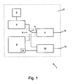
- An in Fig. 1 1 as a whole has a semiconductor component arranged in a component housing semiconductor chip 2 into which a magnetic field-sensitive sensor element 3, namely a Hall plate, and an evaluation device 4 are integrated therefor.
- a power source 5 is integrated, which is connected for feeding a Hall plate current in the sensor element 3 with this.
- the semiconductor component 1 has an operating switching device 6, by means of which it can be brought into a first and a second operating mode.
- a measurement signal output dependent on the magnetic flux density passing through the sensor element 3 is applied to a measuring signal output of the sensor element 3.
- the operation switching device 6 has a switching element 7, which connects the measuring signal output to an input terminal 11 of the evaluation device 4 in the first mode.
- the input terminal 11 is connected to a terminal 12, not shown in detail in the drawing, which is externally accessible to the component housing.
- the switching element 7 is switched such that the signal path between the measuring signal output of the sensor element 3 and the input terminal 11 of the evaluation device 4 is interrupted.
- the input terminal 11 is connected via the switching element 7 to a test signal output of a test signal source 8.
- the test signal source 8 is integrated in the semiconductor chip 2.
- the test signal is generated by means of an external test signal source and applied to the input terminal 11 of the evaluation device 4 via connection contacts provided on the semiconductor component.
- the test signal source 8 has a non-volatile data memory 9, in which a parameter for the sensitivity of the sensor element 3 is stored.
- the characteristic quantity is determined by measurement in the production of the semiconductor wafer from which the semiconductor chip of the sensor element 3 is produced.
- the semiconductor wafer has taps for connecting a measuring current source with the help of the measuring current source, an electric current is generated and fed via the taps in the sensor element 3.
- the voltage drop caused by the current flow in the sensor element 3 is measured, and from the current and the voltage drop, the electrical resistance of the sensor element is determined.
- This is stored in the data memory 9, which may be a PROM, for example.
- the test signal source 8 has an adjusting device not shown in the drawing, by means of which the amplitude of the test signal is adjustable.
- the adjusting device is connected via a serial interface 10 to an external terminal 13 of the semiconductor device 1.
- nominal values for a magnetic flux density to be simulated can be transmitted to the setting device by means of a test device connected to the external connection 13.
- the amplitude of the test signal is adjusted such that the test signal corresponds to the measurement signal of the sensor element 3, which would be present at the input terminal 11 of the evaluation device, if the semiconductor device 1 would be operated in the first mode and the sensor element 3 in a magnetic field, the magnetic Flux density corresponds to the setpoint.
- the test signal source 8 therefore, the measurement signal of the sensor element 3 can be reproduced exactly.
- the interface 10 is connected to an operating mode switching device 6 for this purpose.
- the sensor element 3 is insensitive to magnetic fields in the second operating mode.
- the operating switching device 6 has a first switching element 7a via which the current source 5 is connected to a Hall plate current connection of the sensor element 3.
- the first switching element 7a is connected such that the sensor element 3 is traversed by a Hall plate current.
- the second mode of operation the flow of current to the Hall plate power connections is interrupted.
- the operating switching device 6 further has a second switching element 7b, which is arranged in the signal path between the test signal output of the test signal source and the input terminal 11 of the evaluation device 4.
- a second switching element 7b which is arranged in the signal path between the test signal output of the test signal source and the input terminal 11 of the evaluation device 4.
- the signal path between the test signal output and the input terminal 11 of the evaluation device 4 is interrupted, and in the second operating mode the test signal output is connected to the input terminal 11 of the evaluation device 4.
Landscapes
- Physics & Mathematics (AREA)
- General Physics & Mathematics (AREA)
- Engineering & Computer Science (AREA)
- General Engineering & Computer Science (AREA)
- Electromagnetism (AREA)
- Computer Hardware Design (AREA)
- Microelectronics & Electronic Packaging (AREA)
- Condensed Matter Physics & Semiconductors (AREA)
- Hall/Mr Elements (AREA)
- Measuring Magnetic Variables (AREA)
- Semiconductor Integrated Circuits (AREA)
- Testing Or Calibration Of Command Recording Devices (AREA)
Claims (7)
- Composant semi-conducteur (1) présentant sur une microplaquette semi-conductrice (2), au moins un élément capteur (3) pour mesurer une grandeur physique et un dispositif d'analyse (4), dans lequel le composant semi-conducteur (1) est commutable entre un premier et un deuxième mode de fonctionnement qui est à chaque fois configuré de manière que dans le premier mode de fonctionnement, l'élément capteur (3) est relié au moyen d'une source de courant (5) et sensible à la grandeur physique à mesurer et de manière à ce qu'une sortie de signal de mesure de l'élément capteur (3) étant reliée à une connexion d'entrée (11) du dispositif d'analyse (4)
caractérisé en ce qu'une caractéristique que l'élément capteur présente par rapport à la grandeur à mesurer est sauvegardée dans une mémoire de données (9) et en ce que dans le deuxième mode de fonctionnement, l'élément capteur (3) est insensible à la grandeur physique à mesurer, la liaison entre la source de courant (5) et/ou le chemin du signal entre la sortie du signal de mesure de l'élément capteur (3) et la connexion d'entrée (11) étant interrompue et caractérisé par une source de signal test (8) prévue sur la microplaquette semi-conductrice (2) pour la génération d'un signal test simulé dépendant de la caractéristique mise en mémoire du signal de mesure de l'élément capteur (3) et en ce que le signal test et la source de signal (8) sont reliés à la connexion d'entrée (11) du dispositif d'analyse (4) dans le deuxième mode de fonctionnement pour récréer le signal du capteur à l'aide du signal test. - Composant semi-conducteur (1) selon la revendication 1 caractérisé en ce que la source de signal test (8) présente une station de réglage pour le signal test, et en ce que l'entrée de commande de la station de réglage est reliée directement ou indirectement à travers un dispositif d'excitation comportant une connexion externe du composant semi-conducteur pour le réglage du signal de test.
- Composant semi-conducteur (1) selon la revendication 1 ou la revendication 2 caractérisé en ce que la station de réglage est reliée à une sous-station série (10) à qui par une connexion externe peut être transmis des codes de commande pour le réglage du signal de test.
- Composant semi-conducteur (1) selon l'une des revendications 1 à 3 caractérisé en ce que la sous-station série (10) est reliée à un dispositif de commutation (6) pour commuter le mode de fonctionnement du composant semi-conducteur (1).
- Composant semi-conducteur (1) selon l'une des revendications 1 à 4 caractérisé en ce que l'élément capteur (3) est un capteur de champ magnétique, en particulier un capteur à effet Hall.
- Procédé pour tester un composant semi-conducteur (1) qui présente sur une microplaquette semi-conductrice (2) au moins un élément capteur (3) pour la mesure d'une grandeur physique et un dispositif d'analyse (4) relié à l'élément de capteur (3) par un chemin de signal
caractérisé en ce que
dans un premier mode de fonctionnement, une caractéristique que l'élément capteur présente par rapport à la grandeur à mesurer, est sauvegardée dans une mémoire, et en ce que dans un deuxième mode de fonctionnement, le chemin du signal est bloqué ou interrompu entre l'élément capteur (3) et le dispositif d'analyse (4) pendant une fonction de test du dispositif d'analyse (4), en ce que l'on génère un signal de test simulant le signal de mesure de l'élément capteur (3) dépendant de la caractéristique mise en mémoire, en ce que le signal test alimente le dispositif d'analyse (4) à la place du signal de mesure et en ce que l'on mesure au moins un signal de sortie du dispositif d'analyse (4) dépendant du signal test. - Procédé selon la revendication 6 caractérisé en ce que pour tester l'élément capteur (3), on génère un courant dans l'élément capteur (3) et on mesure la résistance électrique de l'élément capteur (3).
Applications Claiming Priority (1)
| Application Number | Priority Date | Filing Date | Title |
|---|---|---|---|
| DE102007012214A DE102007012214A1 (de) | 2007-03-12 | 2007-03-12 | Halbleiterbauelement und Verfahren zum Testen eines solchen |
Publications (3)
| Publication Number | Publication Date |
|---|---|
| EP1970720A2 EP1970720A2 (fr) | 2008-09-17 |
| EP1970720A3 EP1970720A3 (fr) | 2010-07-28 |
| EP1970720B1 true EP1970720B1 (fr) | 2011-09-21 |
Family
ID=39495975
Family Applications (1)
| Application Number | Title | Priority Date | Filing Date |
|---|---|---|---|
| EP08004059A Active EP1970720B1 (fr) | 2007-03-12 | 2008-03-05 | Elément semi-conducteur et procédé destiné à tester celui-ci |
Country Status (4)
| Country | Link |
|---|---|
| US (1) | US8378672B2 (fr) |
| EP (1) | EP1970720B1 (fr) |
| AT (1) | ATE525661T1 (fr) |
| DE (1) | DE102007012214A1 (fr) |
Cited By (1)
| Publication number | Priority date | Publication date | Assignee | Title |
|---|---|---|---|---|
| DE102023132611B3 (de) | 2023-11-22 | 2025-01-16 | Tdk-Micronas Gmbh | Elektronisches Bauelement und Verfahren zum Betreiben eines solchen |
Families Citing this family (12)
| Publication number | Priority date | Publication date | Assignee | Title |
|---|---|---|---|---|
| US8216317B2 (en) | 2008-03-31 | 2012-07-10 | Stryker Spine | Spinal implant apparatus and methods |
| EP2163861A1 (fr) * | 2008-09-12 | 2010-03-17 | Siemens Aktiengesellschaft | Appareil de mesure de processus |
| EP2211147B1 (fr) * | 2009-01-23 | 2012-11-28 | Micronas GmbH | Procédé de contrôle du fonctionnement d'une circuit électrique |
| US8425529B2 (en) | 2010-09-30 | 2013-04-23 | Stryker Spine | Instrument for inserting surgical implant with guiding rail |
| US8603175B2 (en) | 2010-09-30 | 2013-12-10 | Stryker Spine | Method of inserting surgical implant with guiding rail |
| US8858637B2 (en) | 2010-09-30 | 2014-10-14 | Stryker Spine | Surgical implant with guiding rail |
| TWI439711B (zh) * | 2011-10-03 | 2014-06-01 | Star Techn Inc | 切換矩陣器及其半導體元件特性之測試系統 |
| DE102011084283A1 (de) * | 2011-10-11 | 2013-04-11 | Robert Bosch Gmbh | Sensoreinheit und Verfahren zur Bandendeprogrammierung einer Sensoreinheit |
| US20140070831A1 (en) * | 2012-08-27 | 2014-03-13 | Advantest Corporation | System and method of protecting probes by using an intelligent current sensing switch |
| CN105093155B (zh) * | 2015-08-25 | 2018-01-16 | 清华大学 | 微机电系统mems磁通门磁强计测试系统及其控制方法 |
| BE1026732B1 (de) * | 2018-10-26 | 2020-06-03 | Phoenix Contact Gmbh & Co | Messgerät |
| US11500010B2 (en) * | 2020-01-17 | 2022-11-15 | Texas Instruments Incorporated | Integrated circuit with current limit testing circuitry |
Family Cites Families (8)
| Publication number | Priority date | Publication date | Assignee | Title |
|---|---|---|---|---|
| DE4226224C2 (de) * | 1992-08-07 | 1994-05-26 | Texas Instruments Deutschland | Auf die Einwirkung einer Kraft ansprechender Sensor |
| DE19539458C2 (de) * | 1995-10-24 | 2001-03-15 | Bosch Gmbh Robert | Sensor mit Testeingang |
| DE19606826A1 (de) * | 1996-02-23 | 1997-08-28 | Knorr Bremse Electronic Gmbh | Verfahren und Vorrichtung zur Überprüfung eines Sensors |
| DE19858868C2 (de) * | 1998-12-19 | 2003-06-18 | Micronas Gmbh | Hallsensor |
| JP3835354B2 (ja) * | 2001-10-29 | 2006-10-18 | ヤマハ株式会社 | 磁気センサ |
| EP1637898A1 (fr) * | 2004-09-16 | 2006-03-22 | Liaisons Electroniques-Mecaniques Lem S.A. | Capteur de champs magnétique à calibration continue |
| DE102005028461A1 (de) | 2005-06-17 | 2006-12-28 | Micronas Gmbh | Verfahren zum Testen eines Wafers, insbesondere Hall-Magnetfeld-Sensors und Wafer bzw. Hallsensor |
| GB0620307D0 (en) * | 2006-10-16 | 2006-11-22 | Ami Semiconductor Belgium Bvba | Auto-calibration of magnetic sensor |
-
2007
- 2007-03-12 DE DE102007012214A patent/DE102007012214A1/de not_active Withdrawn
-
2008
- 2008-03-05 EP EP08004059A patent/EP1970720B1/fr active Active
- 2008-03-05 AT AT08004059T patent/ATE525661T1/de active
- 2008-03-12 US US12/046,833 patent/US8378672B2/en active Active
Cited By (1)
| Publication number | Priority date | Publication date | Assignee | Title |
|---|---|---|---|---|
| DE102023132611B3 (de) | 2023-11-22 | 2025-01-16 | Tdk-Micronas Gmbh | Elektronisches Bauelement und Verfahren zum Betreiben eines solchen |
Also Published As
| Publication number | Publication date |
|---|---|
| DE102007012214A1 (de) | 2008-09-18 |
| EP1970720A2 (fr) | 2008-09-17 |
| EP1970720A3 (fr) | 2010-07-28 |
| US20080224694A1 (en) | 2008-09-18 |
| ATE525661T1 (de) | 2011-10-15 |
| US8378672B2 (en) | 2013-02-19 |
Similar Documents
| Publication | Publication Date | Title |
|---|---|---|
| EP1970720B1 (fr) | Elément semi-conducteur et procédé destiné à tester celui-ci | |
| DE69733789T2 (de) | Hochauflösendes Stromversorgungsprüfsystem | |
| DE102008050018A1 (de) | Integrierte Magnetsensorschaltung mit Testleiter | |
| DE102018119727A1 (de) | Prüfen von MOS-Leistungsschaltern | |
| DE10146204A1 (de) | Schaltungsanordnung zur Spannungsversorgung eines Zweidrahtsensors | |
| DE19917261C5 (de) | Elektromagnetische Durchflußmesseranordnung | |
| EP2623940B1 (fr) | Vérification d'un agencement d'appareil de mesure, agencement d'appareil de mesure correspondant et agencement de vérification | |
| DE10011179A1 (de) | Verfahren zur Ermittlung der Temperatur eines Halbleiter-Chips und Halbleiterchip mit Temperaturmessanordnung | |
| DE112014002911T5 (de) | LED-Treiber mit umfassendem Fehlerschutz | |
| DE102017111410A1 (de) | Messungen in Schaltvorrichtungen | |
| WO2020200644A1 (fr) | Dispositif d'amplification pour l'amplification de courants faibles | |
| EP0250620A1 (fr) | Procédé et dispositif pour tester électriquement des circuits imprimés | |
| DE10355116A1 (de) | Ein- und Ausgangsschaltung eines integrierten Schaltkreises, Verfahren zum Testen eines integrierten Schaltkreises sowie integrierter Schaltkreis mit einer solchen Ein- und Ausgangsschaltung | |
| DE102023208995A1 (de) | Stromgesteuertes Spannungsreglertesten | |
| DE19527487C1 (de) | Schaltungsanordnung zum Prüfen der Funktionsfähigkeit einer Stromüberwachungsschaltung für einen Leistungstransistor | |
| DE102014014309A1 (de) | Verfahren zum Testen eines Signalpfades | |
| WO2020233937A1 (fr) | Dispositif et procédé de commande de courant d'un actionneur | |
| DE102007007339B4 (de) | Verfahren und Vorrichtung zum Lokalisieren von Fehlern auf elektronischen Leiterplatten | |
| DE102004049084A1 (de) | Sensorschnittstelle mit integrierter Strommessung | |
| EP0705439B1 (fr) | Procede et dispositif permettant de tester un circuit integre brase sur une platine | |
| DE10341836B4 (de) | Testvorrichtung zum Testen von elektrischen Schaltungen sowie Verfahren zum parallelen Testen von elektrischen Schaltungen | |
| EP3586164A1 (fr) | Dispositif de détection muni d'un capteur pour effectuer une détection d'environnement au moyen d'ondes sonores | |
| DE102013210002A1 (de) | Verfahren und Vorrichtung zum Erkennen eines Fehlers in einer Brückenschaltung | |
| DE102018122314B3 (de) | Anordnung zur Bestimmung eines Gesamtstroms in einer Leitung | |
| EP3652860B1 (fr) | Convertisseur de niveau et procédé de conversion de valeurs de niveau dans des dispositifs de commande de véhicule |
Legal Events
| Date | Code | Title | Description |
|---|---|---|---|
| PUAI | Public reference made under article 153(3) epc to a published international application that has entered the european phase |
Free format text: ORIGINAL CODE: 0009012 |
|
| AK | Designated contracting states |
Kind code of ref document: A2 Designated state(s): AT BE BG CH CY CZ DE DK EE ES FI FR GB GR HR HU IE IS IT LI LT LU LV MC MT NL NO PL PT RO SE SI SK TR |
|
| AX | Request for extension of the european patent |
Extension state: AL BA MK RS |
|
| PUAL | Search report despatched |
Free format text: ORIGINAL CODE: 0009013 |
|
| AK | Designated contracting states |
Kind code of ref document: A3 Designated state(s): AT BE BG CH CY CZ DE DK EE ES FI FR GB GR HR HU IE IS IT LI LT LU LV MC MT NL NO PL PT RO SE SI SK TR |
|
| AX | Request for extension of the european patent |
Extension state: AL BA MK RS |
|
| 17P | Request for examination filed |
Effective date: 20110202 |
|
| AKX | Designation fees paid |
Designated state(s): AT BE BG CH CY CZ DE DK EE ES FI FR GB GR HR HU IE IS IT LI LT LU LV MC MT NL NO PL PT RO SE SI SK TR |
|
| GRAP | Despatch of communication of intention to grant a patent |
Free format text: ORIGINAL CODE: EPIDOSNIGR1 |
|
| RIC1 | Information provided on ipc code assigned before grant |
Ipc: G01R 35/00 20060101ALI20110426BHEP Ipc: G01R 33/00 20060101ALI20110426BHEP Ipc: G01R 31/28 20060101AFI20110426BHEP |
|
| GRAS | Grant fee paid |
Free format text: ORIGINAL CODE: EPIDOSNIGR3 |
|
| GRAA | (expected) grant |
Free format text: ORIGINAL CODE: 0009210 |
|
| AK | Designated contracting states |
Kind code of ref document: B1 Designated state(s): AT BE BG CH CY CZ DE DK EE ES FI FR GB GR HR HU IE IS IT LI LT LU LV MC MT NL NO PL PT RO SE SI SK TR |
|
| REG | Reference to a national code |
Ref country code: GB Ref legal event code: FG4D Free format text: NOT ENGLISH |
|
| REG | Reference to a national code |
Ref country code: CH Ref legal event code: EP |
|
| REG | Reference to a national code |
Ref country code: IE Ref legal event code: FG4D Free format text: LANGUAGE OF EP DOCUMENT: GERMAN |
|
| REG | Reference to a national code |
Ref country code: DE Ref legal event code: R096 Ref document number: 502008004923 Country of ref document: DE Effective date: 20111215 |
|
| REG | Reference to a national code |
Ref country code: NL Ref legal event code: VDEP Effective date: 20110921 |
|
| PG25 | Lapsed in a contracting state [announced via postgrant information from national office to epo] |
Ref country code: FI Free format text: LAPSE BECAUSE OF FAILURE TO SUBMIT A TRANSLATION OF THE DESCRIPTION OR TO PAY THE FEE WITHIN THE PRESCRIBED TIME-LIMIT Effective date: 20110921 Ref country code: LT Free format text: LAPSE BECAUSE OF FAILURE TO SUBMIT A TRANSLATION OF THE DESCRIPTION OR TO PAY THE FEE WITHIN THE PRESCRIBED TIME-LIMIT Effective date: 20110921 Ref country code: NO Free format text: LAPSE BECAUSE OF FAILURE TO SUBMIT A TRANSLATION OF THE DESCRIPTION OR TO PAY THE FEE WITHIN THE PRESCRIBED TIME-LIMIT Effective date: 20111221 Ref country code: SE Free format text: LAPSE BECAUSE OF FAILURE TO SUBMIT A TRANSLATION OF THE DESCRIPTION OR TO PAY THE FEE WITHIN THE PRESCRIBED TIME-LIMIT Effective date: 20110921 Ref country code: HR Free format text: LAPSE BECAUSE OF FAILURE TO SUBMIT A TRANSLATION OF THE DESCRIPTION OR TO PAY THE FEE WITHIN THE PRESCRIBED TIME-LIMIT Effective date: 20110921 |
|
| LTIE | Lt: invalidation of european patent or patent extension |
Effective date: 20110921 |
|
| PG25 | Lapsed in a contracting state [announced via postgrant information from national office to epo] |
Ref country code: LV Free format text: LAPSE BECAUSE OF FAILURE TO SUBMIT A TRANSLATION OF THE DESCRIPTION OR TO PAY THE FEE WITHIN THE PRESCRIBED TIME-LIMIT Effective date: 20110921 Ref country code: CY Free format text: LAPSE BECAUSE OF FAILURE TO SUBMIT A TRANSLATION OF THE DESCRIPTION OR TO PAY THE FEE WITHIN THE PRESCRIBED TIME-LIMIT Effective date: 20110921 Ref country code: GR Free format text: LAPSE BECAUSE OF FAILURE TO SUBMIT A TRANSLATION OF THE DESCRIPTION OR TO PAY THE FEE WITHIN THE PRESCRIBED TIME-LIMIT Effective date: 20111222 Ref country code: SI Free format text: LAPSE BECAUSE OF FAILURE TO SUBMIT A TRANSLATION OF THE DESCRIPTION OR TO PAY THE FEE WITHIN THE PRESCRIBED TIME-LIMIT Effective date: 20110921 |
|
| REG | Reference to a national code |
Ref country code: IE Ref legal event code: FD4D |
|
| PG25 | Lapsed in a contracting state [announced via postgrant information from national office to epo] |
Ref country code: IE Free format text: LAPSE BECAUSE OF FAILURE TO SUBMIT A TRANSLATION OF THE DESCRIPTION OR TO PAY THE FEE WITHIN THE PRESCRIBED TIME-LIMIT Effective date: 20110921 Ref country code: CZ Free format text: LAPSE BECAUSE OF FAILURE TO SUBMIT A TRANSLATION OF THE DESCRIPTION OR TO PAY THE FEE WITHIN THE PRESCRIBED TIME-LIMIT Effective date: 20110921 Ref country code: IS Free format text: LAPSE BECAUSE OF FAILURE TO SUBMIT A TRANSLATION OF THE DESCRIPTION OR TO PAY THE FEE WITHIN THE PRESCRIBED TIME-LIMIT Effective date: 20120121 Ref country code: SK Free format text: LAPSE BECAUSE OF FAILURE TO SUBMIT A TRANSLATION OF THE DESCRIPTION OR TO PAY THE FEE WITHIN THE PRESCRIBED TIME-LIMIT Effective date: 20110921 |
|
| PG25 | Lapsed in a contracting state [announced via postgrant information from national office to epo] |
Ref country code: IT Free format text: LAPSE BECAUSE OF FAILURE TO SUBMIT A TRANSLATION OF THE DESCRIPTION OR TO PAY THE FEE WITHIN THE PRESCRIBED TIME-LIMIT Effective date: 20110921 Ref country code: PT Free format text: LAPSE BECAUSE OF FAILURE TO SUBMIT A TRANSLATION OF THE DESCRIPTION OR TO PAY THE FEE WITHIN THE PRESCRIBED TIME-LIMIT Effective date: 20120123 Ref country code: EE Free format text: LAPSE BECAUSE OF FAILURE TO SUBMIT A TRANSLATION OF THE DESCRIPTION OR TO PAY THE FEE WITHIN THE PRESCRIBED TIME-LIMIT Effective date: 20110921 Ref country code: RO Free format text: LAPSE BECAUSE OF FAILURE TO SUBMIT A TRANSLATION OF THE DESCRIPTION OR TO PAY THE FEE WITHIN THE PRESCRIBED TIME-LIMIT Effective date: 20110921 Ref country code: PL Free format text: LAPSE BECAUSE OF FAILURE TO SUBMIT A TRANSLATION OF THE DESCRIPTION OR TO PAY THE FEE WITHIN THE PRESCRIBED TIME-LIMIT Effective date: 20110921 Ref country code: NL Free format text: LAPSE BECAUSE OF FAILURE TO SUBMIT A TRANSLATION OF THE DESCRIPTION OR TO PAY THE FEE WITHIN THE PRESCRIBED TIME-LIMIT Effective date: 20110921 |
|
| PLBE | No opposition filed within time limit |
Free format text: ORIGINAL CODE: 0009261 |
|
| STAA | Information on the status of an ep patent application or granted ep patent |
Free format text: STATUS: NO OPPOSITION FILED WITHIN TIME LIMIT |
|
| PG25 | Lapsed in a contracting state [announced via postgrant information from national office to epo] |
Ref country code: DK Free format text: LAPSE BECAUSE OF FAILURE TO SUBMIT A TRANSLATION OF THE DESCRIPTION OR TO PAY THE FEE WITHIN THE PRESCRIBED TIME-LIMIT Effective date: 20110921 |
|
| 26N | No opposition filed |
Effective date: 20120622 |
|
| BERE | Be: lapsed |
Owner name: MICRONAS G.M.B.H. Effective date: 20120331 |
|
| REG | Reference to a national code |
Ref country code: DE Ref legal event code: R097 Ref document number: 502008004923 Country of ref document: DE Effective date: 20120622 |
|
| PG25 | Lapsed in a contracting state [announced via postgrant information from national office to epo] |
Ref country code: MC Free format text: LAPSE BECAUSE OF NON-PAYMENT OF DUE FEES Effective date: 20120331 |
|
| REG | Reference to a national code |
Ref country code: CH Ref legal event code: PL |
|
| PG25 | Lapsed in a contracting state [announced via postgrant information from national office to epo] |
Ref country code: LI Free format text: LAPSE BECAUSE OF NON-PAYMENT OF DUE FEES Effective date: 20120331 Ref country code: BE Free format text: LAPSE BECAUSE OF NON-PAYMENT OF DUE FEES Effective date: 20120331 Ref country code: CH Free format text: LAPSE BECAUSE OF NON-PAYMENT OF DUE FEES Effective date: 20120331 |
|
| PG25 | Lapsed in a contracting state [announced via postgrant information from national office to epo] |
Ref country code: ES Free format text: LAPSE BECAUSE OF FAILURE TO SUBMIT A TRANSLATION OF THE DESCRIPTION OR TO PAY THE FEE WITHIN THE PRESCRIBED TIME-LIMIT Effective date: 20120101 |
|
| PG25 | Lapsed in a contracting state [announced via postgrant information from national office to epo] |
Ref country code: BG Free format text: LAPSE BECAUSE OF FAILURE TO SUBMIT A TRANSLATION OF THE DESCRIPTION OR TO PAY THE FEE WITHIN THE PRESCRIBED TIME-LIMIT Effective date: 20111221 |
|
| PG25 | Lapsed in a contracting state [announced via postgrant information from national office to epo] |
Ref country code: MT Free format text: LAPSE BECAUSE OF FAILURE TO SUBMIT A TRANSLATION OF THE DESCRIPTION OR TO PAY THE FEE WITHIN THE PRESCRIBED TIME-LIMIT Effective date: 20110921 |
|
| PG25 | Lapsed in a contracting state [announced via postgrant information from national office to epo] |
Ref country code: TR Free format text: LAPSE BECAUSE OF FAILURE TO SUBMIT A TRANSLATION OF THE DESCRIPTION OR TO PAY THE FEE WITHIN THE PRESCRIBED TIME-LIMIT Effective date: 20110921 |
|
| REG | Reference to a national code |
Ref country code: AT Ref legal event code: MM01 Ref document number: 525661 Country of ref document: AT Kind code of ref document: T Effective date: 20130305 |
|
| PG25 | Lapsed in a contracting state [announced via postgrant information from national office to epo] |
Ref country code: LU Free format text: LAPSE BECAUSE OF NON-PAYMENT OF DUE FEES Effective date: 20120305 |
|
| PG25 | Lapsed in a contracting state [announced via postgrant information from national office to epo] |
Ref country code: HU Free format text: LAPSE BECAUSE OF FAILURE TO SUBMIT A TRANSLATION OF THE DESCRIPTION OR TO PAY THE FEE WITHIN THE PRESCRIBED TIME-LIMIT Effective date: 20080305 |
|
| PG25 | Lapsed in a contracting state [announced via postgrant information from national office to epo] |
Ref country code: AT Free format text: LAPSE BECAUSE OF NON-PAYMENT OF DUE FEES Effective date: 20130305 |
|
| REG | Reference to a national code |
Ref country code: FR Ref legal event code: PLFP Year of fee payment: 9 |
|
| REG | Reference to a national code |
Ref country code: DE Ref legal event code: R082 Ref document number: 502008004923 Country of ref document: DE Representative=s name: KOCH-MUELLER PATENTANWALTSGESELLSCHAFT MBH, DE Ref country code: DE Ref legal event code: R081 Ref document number: 502008004923 Country of ref document: DE Owner name: TDK-MICRONAS GMBH, DE Free format text: FORMER OWNER: MICRONAS GMBH, 79108 FREIBURG, DE |
|
| REG | Reference to a national code |
Ref country code: FR Ref legal event code: PLFP Year of fee payment: 10 |
|
| REG | Reference to a national code |
Ref country code: FR Ref legal event code: PLFP Year of fee payment: 11 |
|
| REG | Reference to a national code |
Ref country code: FR Ref legal event code: CD Owner name: TDK-MICRONAS GMBH, DE Effective date: 20180717 |
|
| PGFP | Annual fee paid to national office [announced via postgrant information from national office to epo] |
Ref country code: GB Payment date: 20200323 Year of fee payment: 13 |
|
| PGFP | Annual fee paid to national office [announced via postgrant information from national office to epo] |
Ref country code: FR Payment date: 20200319 Year of fee payment: 13 |
|
| GBPC | Gb: european patent ceased through non-payment of renewal fee |
Effective date: 20210305 |
|
| PG25 | Lapsed in a contracting state [announced via postgrant information from national office to epo] |
Ref country code: FR Free format text: LAPSE BECAUSE OF NON-PAYMENT OF DUE FEES Effective date: 20210331 Ref country code: GB Free format text: LAPSE BECAUSE OF NON-PAYMENT OF DUE FEES Effective date: 20210305 |
|
| PGFP | Annual fee paid to national office [announced via postgrant information from national office to epo] |
Ref country code: DE Payment date: 20260319 Year of fee payment: 19 |