EP1973287A1 - System zur Demodulation von Phasenumtastungssignalen - Google Patents
System zur Demodulation von Phasenumtastungssignalen Download PDFInfo
- Publication number
- EP1973287A1 EP1973287A1 EP07380075A EP07380075A EP1973287A1 EP 1973287 A1 EP1973287 A1 EP 1973287A1 EP 07380075 A EP07380075 A EP 07380075A EP 07380075 A EP07380075 A EP 07380075A EP 1973287 A1 EP1973287 A1 EP 1973287A1
- Authority
- EP
- European Patent Office
- Prior art keywords
- signals
- outputs
- signal
- argument
- output
- Prior art date
- Legal status (The legal status is an assumption and is not a legal conclusion. Google has not performed a legal analysis and makes no representation as to the accuracy of the status listed.)
- Withdrawn
Links
- 230000010363 phase shift Effects 0.000 title claims abstract description 10
- 230000008859 change Effects 0.000 claims description 9
- 238000001914 filtration Methods 0.000 claims description 3
- 230000004044 response Effects 0.000 description 7
- 238000006243 chemical reaction Methods 0.000 description 6
- 238000002955 isolation Methods 0.000 description 6
- 238000010586 diagram Methods 0.000 description 5
- 238000000034 method Methods 0.000 description 5
- 230000001427 coherent effect Effects 0.000 description 3
- 230000008901 benefit Effects 0.000 description 2
- 230000000694 effects Effects 0.000 description 2
- 230000036039 immunity Effects 0.000 description 2
- 230000008569 process Effects 0.000 description 2
- 101100171060 Caenorhabditis elegans div-1 gene Proteins 0.000 description 1
- 239000000654 additive Substances 0.000 description 1
- 230000000996 additive effect Effects 0.000 description 1
- 230000003321 amplification Effects 0.000 description 1
- 238000004458 analytical method Methods 0.000 description 1
- 230000007274 generation of a signal involved in cell-cell signaling Effects 0.000 description 1
- 238000002347 injection Methods 0.000 description 1
- 239000007924 injection Substances 0.000 description 1
- 230000007257 malfunction Effects 0.000 description 1
- 238000003199 nucleic acid amplification method Methods 0.000 description 1
- 238000012805 post-processing Methods 0.000 description 1
- 238000007781 pre-processing Methods 0.000 description 1
- 230000008929 regeneration Effects 0.000 description 1
- 238000011069 regeneration method Methods 0.000 description 1
- 230000007704 transition Effects 0.000 description 1
Images


Classifications
-
- H—ELECTRICITY
- H04—ELECTRIC COMMUNICATION TECHNIQUE
- H04L—TRANSMISSION OF DIGITAL INFORMATION, e.g. TELEGRAPHIC COMMUNICATION
- H04L27/00—Modulated-carrier systems
- H04L27/18—Phase-modulated carrier systems, i.e. using phase-shift keying
- H04L27/22—Demodulator circuits; Receiver circuits
-
- H—ELECTRICITY
- H04—ELECTRIC COMMUNICATION TECHNIQUE
- H04L—TRANSMISSION OF DIGITAL INFORMATION, e.g. TELEGRAPHIC COMMUNICATION
- H04L27/00—Modulated-carrier systems
- H04L27/18—Phase-modulated carrier systems, i.e. using phase-shift keying
- H04L27/22—Demodulator circuits; Receiver circuits
- H04L27/233—Demodulator circuits; Receiver circuits using non-coherent demodulation
Definitions
- This invention generally relates to a system for demodulation of phase shift keying signals (PSK), whether they are digital Binary PSK signals (BPSK), Quadrature PSK signals (QPSK) or M-ary PSK signals (MPSK).
- PSK phase shift keying signals
- BPSK digital Binary PSK signals
- QPSK Quadrature PSK signals
- MPSK M-ary PSK signals
- the invention particularly relates to a system for demodulation of PSK signals which takes advantage from the effects that the locking of resonant circuits by superharmonic injection produce, together with the interference phenomena, and more particularly it relates to a demodulation system which is designed to avoid mutual locking between said resonant circuits.
- the general application fields of the invention are digital communications, particularly wireless digital communications.
- PSK sinusoidal signal
- FSK Frequency Shift Keying
- ASK Amplitude Shift Keying
- the simplest PSK signal is the Binary PSK signal (BPSK).
- BPSK signals can be easily obtained by multiplying the carrier by +1 (0° phase state) or by -1 (180° phase state). From the receiver point of view, it is impossible to know if the phase of an incoming BPSK signal corresponds to 0° state or to 180° state. This is due to the fact that the actual propagation path from the emitter to the receiver is usually unknown. To avoid this indetermination, the information to be transmitted is coded as transitions between phase states, instead of being coded as fixed phase values.
- the usual procedure for demodulating BPSK signals is that of coherent demodulation.
- the demodulation process consists of multiplying the received signal by a reference signal at the same frequency as the original carrier.
- WO-A-03079624 was proposed to overcome the by then state of the art, and the invention there described presents the advantages of coherent demodulation (input signal tracking and demodulation process which is independent of the modulating signal bit period), but without the requirement for the explicit use of a frequency and phase locking loop (PLL or Costas loop).
- PLL frequency and phase locking loop
- the system proposed in WO-A-03079624 is a converter of digital phase modulation (PSK) signals into digital amplitude (ASK) signals.
- PSK digital phase modulation
- ASK digital amplitude
- ASK modulation is the simplest modulation scheme, both from the signal generation point of view and its demodulation, however, it is not very efficient with regards to noise immunity.
- the information contained in an ASK signal is transmitted by modifying the amplitude between two pre-established values.
- Demodulation of these signal is very simple as it only requires an envelope detector, for example, a diode and lowpass filter, followed by amplification and/or signal regeneration as necessary ( Fig. 1 ).
- envelope detector for example, a diode and lowpass filter
- signal regeneration as necessary ( Fig. 1 ).
- the simplicity of ASK signal demodulation makes it useful to have signal converters available with a more efficient modulation with respect to noise, for example, FSK or BPSK and ASK signals.
- the invention proposed by WO-A-03079624 concerns to a system and method for the conversion of digital phase modulated (PSK) signals into digital amplitude modulation (ASK) signals by using a power divider with an input injected with a PSK signal, the outputs of which are connected to at least two argument/frequency dividers having each one a natural tuneable resonant frequency, the output signals of which have a phase difference depending on the phase changes of the input signal, which for example is of 0° or 180° in the case of BPSK conversion or of 90°, 180° and 270° in the case of QPSK conversion.
- the argument/frequency dividers outputs are connected to the inputs of at least a power combiner, the output of which is the sum of the at least two argument/frequency dividers output signals.
- a BPSK to ASK converter see Fig. 2
- additive interference takes place in the combiner, and when this difference is, for example, 180°, a subtractive interference occurs, so that the result is an ASK signal.
- the proposed system is extrapolable to phase modulation with a greater number of symbols, not only to the mentioned QPSK signals but also to M-PSK modulation.
- the present invention concerns to a system for demodulation of phase shift keying signals, or PSK signals, of the type which comprises some elements in common with said proposal of WO-A-03079624 , which are:
- the system proposed by the present invention differs from the proposed by WO-A-03079624 in that alternatively to using a power combiner in said output stage, it has an output stage which is adapted to isolate said argument/frequency dividers outputs in order to avoid mutual locking between said argument/frequency dividers, for which it comprises at least M-1 devices acting at least as analogue multipliers providing at their outputs M-1 signals each of them containing at least harmonic components of one of the M-1 base-band signals which were used to modulate said PSK signal.
- Suitable filters are also included in said output stage to recover said base band signal, or signals, as well as possible, and so complete the demodulation of said PSK signal without the need of using additional circuits.
- Those filters can be part of said device, or devices, which act as analogue multipliers, or be external to them and connected to their outputs.
- Those devices which act at least as analogue multipliers are preferably those which are commonly denominated "mixers" which properties referred to isolation between their inputs to avoid said mutual locking of the ILOs connected thereto are much better than those of a power combiner, as any person skilled in the art knows.
- the system proposed comprises several of those mixers connected interspersed between different electrical paths between the input (or inputs) and the output (or outputs) of the system or demodulator proposed, being said paths responsible of electrically space out said ILOs outputs, and thereby contribute to said isolation and avoidance of said mutual locking.
- Figures 1 and 2 deal with the state of the art and have already been described in the background section and also in WO-A-03079624 , which, as already said above, is wholly included herein by reference.
- the present invention concerns to a system for demodulation of phase shift keying signals, or PSK signals, whether they are BPSK, QPSK or any MPSK signals.
- Figs. 3 and 7 refers to embodiments of the system proposed by the present invention for demodulating BPSK signals, and correspond to the simplest possible arrangements to simplify the description and explanation of the invention, but they completely extrapolable to MP ⁇ SK -demodulators, by using the same elements only increased in number and connected properly.
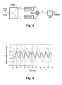
- FIG. 3 The diagram shown in Fig. 3 comprises the following sections:
- Fig. 4 shows the time domain waveforms of the injected BPSK signal (continuous line), argument/frequency dividers output signals O 2 (dotted line) and O 1 (dashed line) around one of the times at which the input phase changes. Note that the phase change in 180° of BPSK signal induces a phase change in 90° in O 2 signal and -90° in O 1 signal. Consequently, O 2 and O 1 signals, originally in counter phase, become in phase after the phase change of the BPSK signal injected at the Input terminal of the arrangement, or demodulator, shown in Fig. 3 .
- Said argument/frequency dividers Div1, Div2 are substantially identical, producing architectural symmetry and determining that their output signals O 1 , O 2 are equal in both power and frequency
- the characteristic part of the present invention is that alternative to just summing said argument/frequency dividers output signals O 1 and O 2 by using a power combiner (as in WO-A-03079624 ), a different kind of output stage is proposed which assures that mutual locking between said argument/frequency dividers Div 1 , Div 2 is not produced, and also than a complete demodulation of the PSK signal is accomplished.
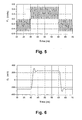
- said output stage comprises one device MixF 1 acting at least as analogue multipliers, which has two inputs connected each one to each of said argument/frequency dividers outputs, in order to at least multiply said argument/frequency dividers output signals O 1 , O 2 , for providing a signal F 1 which contains at least harmonic components of the base-band signal used to modulate said BPSK signal, and which is represented by Fig. 5 .
- Said F 1 signal is ideally the analogue product of O 2 and O 1 .
- the arrangement there illustrated also comprises a low pass filter LPF 1 for filtering said signal F 1 represented in Fig. 5 , in order to provide at its output a signal E 1 which contains substantially only said harmonic components of the base-band signal.
- Said E 1 signal is represented by Fig. 6 , and is the signal finally provided by the demodulator represented in Fig. 3 , at its Output terminal.
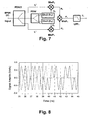
- Fig. 7 illustrates a further arrangement representative of another embodiment of the present invention. It comprises all the elements of Fig. 3 arrangement, but it offers additional isolation to the argument/frequency dividers outputs.
- an additional power divider PDIV2 with an input to be injected with the same BPSK signal injected to said power divider PDIV, and with two outputs, from which corresponding output signals i' 1 , i' 2 , equal to said power divider output signals i 1 , i 2 , are obtained, one per output.
- the output stage of the arrangement of Fig. 7 comprises two additional devices MixP 1 , MixP 2 equal to said device MixF 1 .
- each of said two additional devices MixP 1 , MixP 2 has one of their inputs connected to one of the outputs of the argument/frequency dividers Div 1 , Div 2 , and the other input connected to one of the outputs of said additional power divider PDIV2 in order to at least multiply, each of said additional devices MixP 1 , MixP 2 , one of said argument/frequency dividers output signals O 1 , O 2 per one of said additional power divider output signals i' 1 , i' 2 , providing two output signals P 1 , P 2 as a result of said multiplications.
- Fig. 8 shows the time domain waveforms of signals P 2 (dotted line) and P 1 (dashed line), which are ideally just the product between the BPSK signal injected at the Input terminal and signals O 2 and O 1 , respectively.
- the demodulator shown in Fig. 7 has also one of said devices MixF 1 whose two inputs are connected, respectively, to said two additional devices outputs, in order to at least multiply said output signals P 1 , P 2 coming there from, for providing said signal F 1 which contains at least said harmonic components of the base-band signal used to modulate the BPSK injected signal, and which is represented by Fig. 9 .
- Said F 1 signal is ideally the analogue product of P 2 and P 1 .
- the arrangement there illustrated also comprises a low pass filter LPF 1 for filtering said signal F 1 represented in Fig. 9 , in order to provide at its output a signal E 1 which contains substantially only said harmonic components of the base-band signal.
- Said E 1 signal is represented by Fig. 10 , and is the signal finally provided by the demodulator represented in Fig. 7 , at its Output terminal.
- circuit there represented could further include additional filters at said additional devices outputs, in order to properly filter said signals P 1 , P 2 prior to be multiplied by MixF 1 .
- the low pass filters LPF 1 has been represented as an independent block external to said device MixF 1 , for other embodiments (not shown) it could be part of it, acting therefore said device MixF 1 as a multiplier and also as a low pass filter.
- said device MixF 1 and said additional device MixP 1 are what are commonly known by mixers.
- any of the two arrangements described just above would be injected, at their Input terminal, with a signal with quadrature phase shift keying, or QPSK, modulation, the system would perform a demodulation of it to finally obtain three signals, at their Output terminals, each of them containing at least harmonic components of the three base-band signals which were used to modulate said QPSK signal.
- QPSK quadrature phase shift keying
Landscapes
- Engineering & Computer Science (AREA)
- Computer Networks & Wireless Communication (AREA)
- Signal Processing (AREA)
- Digital Transmission Methods That Use Modulated Carrier Waves (AREA)
Priority Applications (1)
| Application Number | Priority Date | Filing Date | Title |
|---|---|---|---|
| EP07380075A EP1973287A1 (de) | 2007-03-19 | 2007-03-19 | System zur Demodulation von Phasenumtastungssignalen |
Applications Claiming Priority (1)
| Application Number | Priority Date | Filing Date | Title |
|---|---|---|---|
| EP07380075A EP1973287A1 (de) | 2007-03-19 | 2007-03-19 | System zur Demodulation von Phasenumtastungssignalen |
Publications (1)
| Publication Number | Publication Date |
|---|---|
| EP1973287A1 true EP1973287A1 (de) | 2008-09-24 |
Family
ID=38235161
Family Applications (1)
| Application Number | Title | Priority Date | Filing Date |
|---|---|---|---|
| EP07380075A Withdrawn EP1973287A1 (de) | 2007-03-19 | 2007-03-19 | System zur Demodulation von Phasenumtastungssignalen |
Country Status (1)
| Country | Link |
|---|---|
| EP (1) | EP1973287A1 (de) |
Cited By (1)
| Publication number | Priority date | Publication date | Assignee | Title |
|---|---|---|---|---|
| DE102012107079A1 (de) * | 2012-08-02 | 2014-02-06 | Endress + Hauser Conducta Gesellschaft für Mess- und Regeltechnik mbH + Co. KG | Verfahren und elektronische Schaltung zum Demodulieren eines Trägersignals |
Citations (1)
| Publication number | Priority date | Publication date | Assignee | Title |
|---|---|---|---|---|
| US20060023809A1 (en) * | 2002-03-15 | 2006-02-02 | Lopez Villegas Jose M | System for demodulation of phase shift keying signals |
-
2007
- 2007-03-19 EP EP07380075A patent/EP1973287A1/de not_active Withdrawn
Patent Citations (1)
| Publication number | Priority date | Publication date | Assignee | Title |
|---|---|---|---|---|
| US20060023809A1 (en) * | 2002-03-15 | 2006-02-02 | Lopez Villegas Jose M | System for demodulation of phase shift keying signals |
Cited By (1)
| Publication number | Priority date | Publication date | Assignee | Title |
|---|---|---|---|---|
| DE102012107079A1 (de) * | 2012-08-02 | 2014-02-06 | Endress + Hauser Conducta Gesellschaft für Mess- und Regeltechnik mbH + Co. KG | Verfahren und elektronische Schaltung zum Demodulieren eines Trägersignals |
Similar Documents
| Publication | Publication Date | Title |
|---|---|---|
| US7095274B2 (en) | System for demodulation of phase shift keying signals | |
| EP1696623B1 (de) | Verfahren und Vorrichtung zur kohärenten Demodulation von BPSK (binäre Phasensprungmodulation)-Signalen | |
| EP0417528B1 (de) | Breitband-Basisband 90 Phasenschieberschaltung und ein FSK-Radioempfänger, der diese enthält | |
| JPS5831065B2 (ja) | Fsk復調装置 | |
| EP3472989B1 (de) | Verfahren zur modulation und demodulation von psk-signalen und demodulator dafür | |
| EP0412291B1 (de) | Quadraturempfänger für FSK-Signale mit Frequenzverschiebungskompensation | |
| US4528526A (en) | PSK modulator with noncollapsable output for use with a PLL power amplifier | |
| CN107171995B (zh) | Gmsk信号生成装置及方法、信号检测装置及方法 | |
| Rich et al. | Cochannel FM interference suppression using adaptive notch filters | |
| EP0484914A2 (de) | Demodulator und Verfahren zur Demodulation MSK-modulierter, digitaler Signale | |
| EP1973287A1 (de) | System zur Demodulation von Phasenumtastungssignalen | |
| US4744094A (en) | BPSK demodulator with D type flip/flop | |
| JPH0542863B2 (de) | ||
| US4882552A (en) | Coherent frequency exchange keying modulator | |
| JPS6211347A (ja) | 4相psk復調装置 | |
| US4097813A (en) | Carrier wave recovery circuit | |
| US4455680A (en) | Method and apparatus for receiving and tracking phase modulated signals | |
| US6985541B1 (en) | FM demodulator for a low IF receiver | |
| US3971999A (en) | Coherent phase demodulator for phase shift keyed suppressed carrier signals | |
| Feher et al. | A new symbol timing recovery technique for burst modem applications | |
| Gibson et al. | Analog Communications | |
| GB2318229A (en) | Costas loop carrier recovery circuit | |
| KR950003667B1 (ko) | 비.에프.에스.케이(BFSK) 복조방식을 이용한 엠.에스.케이(MSK;minimum shift keying)의 변복조 장치 | |
| CA1066371A (en) | Demodulator for frequency-shift keying system | |
| KR100285756B1 (ko) | 무선전송장비에서캐리어트래킹장치 |
Legal Events
| Date | Code | Title | Description |
|---|---|---|---|
| PUAI | Public reference made under article 153(3) epc to a published international application that has entered the european phase |
Free format text: ORIGINAL CODE: 0009012 |
|
| AK | Designated contracting states |
Kind code of ref document: A1 Designated state(s): AT BE BG CH CY CZ DE DK EE ES FI FR GB GR HU IE IS IT LI LT LU LV MC MT NL PL PT RO SE SI SK TR |
|
| AX | Request for extension of the european patent |
Extension state: AL BA HR MK RS |
|
| STAA | Information on the status of an ep patent application or granted ep patent |
Free format text: STATUS: THE APPLICATION HAS BEEN WITHDRAWN |
|
| 18W | Application withdrawn |
Effective date: 20081016 |