EP1976016A2 - Halbleitervorrichtung - Google Patents
Halbleitervorrichtung Download PDFInfo
- Publication number
- EP1976016A2 EP1976016A2 EP20080153474 EP08153474A EP1976016A2 EP 1976016 A2 EP1976016 A2 EP 1976016A2 EP 20080153474 EP20080153474 EP 20080153474 EP 08153474 A EP08153474 A EP 08153474A EP 1976016 A2 EP1976016 A2 EP 1976016A2
- Authority
- EP
- European Patent Office
- Prior art keywords
- layer
- compound semiconductor
- semiconductor device
- gan
- undoped
- Prior art date
- Legal status (The legal status is an assumption and is not a legal conclusion. Google has not performed a legal analysis and makes no representation as to the accuracy of the status listed.)
- Granted
Links
Images


Classifications
-
- H—ELECTRICITY
- H10—SEMICONDUCTOR DEVICES; ELECTRIC SOLID-STATE DEVICES NOT OTHERWISE PROVIDED FOR
- H10D—INORGANIC ELECTRIC SEMICONDUCTOR DEVICES
- H10D30/00—Field-effect transistors [FET]
- H10D30/40—FETs having zero-dimensional [0D], one-dimensional [1D] or two-dimensional [2D] charge carrier gas channels
- H10D30/47—FETs having zero-dimensional [0D], one-dimensional [1D] or two-dimensional [2D] charge carrier gas channels having two-dimensional [2D] charge carrier gas channels, e.g. nanoribbon FETs or high electron mobility transistors [HEMT]
- H10D30/471—High electron mobility transistors [HEMT] or high hole mobility transistors [HHMT]
- H10D30/473—High electron mobility transistors [HEMT] or high hole mobility transistors [HHMT] having confinement of carriers by multiple heterojunctions, e.g. quantum well HEMT
- H10D30/4732—High electron mobility transistors [HEMT] or high hole mobility transistors [HHMT] having confinement of carriers by multiple heterojunctions, e.g. quantum well HEMT using Group III-V semiconductor material
-
- H—ELECTRICITY
- H10—SEMICONDUCTOR DEVICES; ELECTRIC SOLID-STATE DEVICES NOT OTHERWISE PROVIDED FOR
- H10D—INORGANIC ELECTRIC SEMICONDUCTOR DEVICES
- H10D30/00—Field-effect transistors [FET]
- H10D30/01—Manufacture or treatment
- H10D30/015—Manufacture or treatment of FETs having heterojunction interface channels or heterojunction gate electrodes, e.g. HEMT
-
- H—ELECTRICITY
- H10—SEMICONDUCTOR DEVICES; ELECTRIC SOLID-STATE DEVICES NOT OTHERWISE PROVIDED FOR
- H10D—INORGANIC ELECTRIC SEMICONDUCTOR DEVICES
- H10D62/00—Semiconductor bodies, or regions thereof, of devices having potential barriers
- H10D62/80—Semiconductor bodies, or regions thereof, of devices having potential barriers characterised by the materials
- H10D62/85—Semiconductor bodies, or regions thereof, of devices having potential barriers characterised by the materials being Group III-V materials, e.g. GaAs
- H10D62/8503—Nitride Group III-V materials, e.g. AlN or GaN
Definitions
- the present invention relates to a compound semiconductor device and, more particularly, a compound semiconductor device having a gallium nitride based compound semiconductor layer as an active layer.
- An electronic device such as a GaN based semiconductor device, in which a GaN layer and an AlGaN layer are grown sequentially over a substrate and the GaN layer is used as a channel layer, has been actively developed.
- a sapphire substrate, a SiC substrate, a GaN substrate, a silicon substrate and the like are used as a substrate on which the GaN layer is deposited.
- the GaN layer has an energy bandgap of 3.4 eV that is larger than that of 1.4 eV of the GaAs layer, and is expected to operate in a higher voltage and withstand a higher voltage.
- Japanese Patent Application Publication 2006-114653- A discloses the GaN High Electron Mobility Transistor (HEMT) as a high withstand-voltage GaN electronic device.
- HEMT GaN High Electron Mobility Transistor
- the GaN-HEMT used as an amplifier has a load line characteristic so as to provide high load impedance, and hence can operate very efficiently.
- the GaN-HEMT exhibits a high power density, and hence a chip size of the GaN-HEMT can be reduced, and a power loss in the amplifier can be reduced. Thus, a cost for managing a small amplifier, which provides large load impedance and easiness of impedance matching, can be reduced.
- GaN-HEMT is being developed intensively for a communication system at a higher frequency in a milimeter-wavelength band.
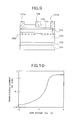
- the conventional GaN-HEMT has a structure shown in FIG. 9 , for example.
- an AlN layer 102, a GaN layer 103, an n-type AlGaN layer 104, and an n-type GaN layer 105 are formed sequentially on a SiC substrate 101.
- the AlN layer 102 and a lower portion of the GaN layer 103 form a buffer layer.
- Ohmic-contacts of a source electrode 107s and a drain electrode 107d which are disposed at a distance are formed on the n-type AlGaN layer 104. Also, Schottky-contact of a gate electrode 108 which is disposed at distances between the source electrode 107s and the drain electrode 107d is formed on the n-type GaN layer 105.
- a silicon nitride layer 106 is formed as a protection insulating film on the n-type GaN layer 105 and between the source electrode 107s and the drain electrode 107d.
- a compound semiconductor device having a transistor structure, including a substrate, a first layer formed over the substrate and comprising GaN, a second layer formed over the first layer and comprising InN whose lattice constant is larger than the first layer, a third layer formed over the second layer and comprising GaN whose energy bandgap is smaller than the second layer, and a channel region layer formed over the third layer.
- the gate length of the gate electrode 108 is about 0.8 ⁇ m in the conventional technique.
- An embodiment a transistor structure comprises a substrate, a first layer formed on the substrate and containing GaN, a second layer formed over the first layer and comprising InN whose lattice constant is larger than the first layer, a third layer formed over the second layer and comprising GaN whose energy bandgap is smaller than the second layer, and a channel region layer formed on the third layer.
- the second layer which is formed below the channel region layer prevents movement of carriers accelerated in a channel region toward the underlying substrate.
- it can be made easy to turn off the current flowing between the drain-source regions by a threshold of a gate voltage. Also, even when a temperature is raised, a movement of the carriers toward the buffer can be suppressed.
- FIGS. 1A to 1C are sectional views showing a compound semiconductor device according to a first embodiment of the present invention and steps of forming the same.
- an AlN layer 2 of 0.3 ⁇ m thickness and an undoped GaN layer 3 of 2.5 ⁇ m thickness are formed as a buffer layer on a single crystal SiC substrate 1.
- a composition ratio y1 in the Al y1 Ga 1-y1 N layer 6 and the Al y1 Ga 1-y1 N layer 7 is set to 0.33, for example.
- Respective layers from the AlN layer 2 to the n-type GaN layer 8 are formed successively by the metal organic vapor-phase epitaxy (MOVPE) method while selecting the material gas respectively.
- MOVPE metal organic vapor-phase epitaxy
- trimethylaluminum, trimethylgallium, and trimethylindium are used as the material of aluminum (Al), as the material of gallium (Ga), and as the material of indium (In) respectively.
- ammonia (NH 3 ) is used as the material of nitrogen (N).
- silicon (Si) is doped in the Al y1 Ga 1-y1 N layer 7 at a concentration of 4 ⁇ 10 18 cm -3 , for example.
- Si is doped in the n-type GaN layer 8 at a concentration of 5x10 18 cm -3 , for example.
- Si is an n-type dopant and, for example, silane is used as the material.
- a silicon nitride (SiN) film 9 serving as a protection insulating film is formed on the n-type GaN layer 8 by the plasma CVD method to have a thickness of about 40 nm, for example.
- the silicon nitride film 9 is patterned by the photolithography method.
- a source opening portion 9s and a drain opening portion 9d are formed in a source region and a drain region respectively.
- the n-type GaN layer 8 is etched by the dry etching through the source opening portion 9s and the drain opening portion 9d.
- the Al y1 Ga 1-y1 N layer 7 is exposed from the source opening portion 9s and the drain opening portion 9d.
- a gas used in the dry etching for example, chlorine (Cl 2 ) is used.
- a photoresist (not shown) is coated on the silicon nitride film 9 and then exposed/developed.
- windows (not shown) are formed on the source opening portion 9s and the drain opening portion 9d respectively.
- a Ti layer of about 30 nm thickness and an Al layer of about 200 nm thickness are formed sequentially on the photoresist and in the windows by the evaporation method.
- the photoresist is removed.
- the Ti layer and the Al layer being left in the source opening portion 9s and the drain opening portion 9d respectively are used as a source electrode 10s and a drain electrode 10d.
- the Ti layer and the Al layer are annealed at 600 °C, for example.
- the source electrode 10s and the drain electrode 10d consisting of these metal layers form ohmic-contacts to the n-type AlGaN layer 7.
- the silicon nitride film 9 is patterned by the photolithography method.
- a gate opening portion 9g is formed in a predetermined position between the source electrode 10s and the drain electrode 10d at intervals from these electrodes 10s and 10d.
- a photoresist (not shown) is coated on the silicon nitride film 9 and is exposed/developed.
- a window (not shown) is formed in a region containing the gate opening portion 9g.
- a nickel (Ni) layer of about 30 nm and a gold (Au) layer of about 400 nm are formed sequentially on the photoresist and the window by the evaporation method.
- the photoresist is removed.
- the Ni layer and the Au layer left in the gate opening portion 9g are used as a gate electrode 11.
- the gate electrode 11 forms Schottky-contact to the n-type GaN layer 8.
- a length in the direction from the source electrode 10s to the drain electrode 10d i.e., a gate length is about 80 nm, for example, and a length perpendicular to the gate length, i.e., a unit gate width is about 50 ⁇ m, for example.
- an element isolation recess is formed by etching the periphery of the element by using a mask.
- high-concentration carriers are generated due to the piezo polarization at a heterojunction interface between the undoped GaN layer 5 and the undoped Al y1 Ga 1-y1 N layer 6, and thus a two-dimensional electron gas (2DEG) is generated.
- 2DEG two-dimensional electron gas
- channel regions are generated in lower and upper interfaces between the undoped GaN layer 5 and the underlying undoped In x1 Al 1-x1 N layer 4 and the overlying undoped Al y1 Ga 1-y1 N layer 6 respectively.
- a concentration of the two-dimensional electron gas is increased.
- the undoped In x1 Al 1-x1 N layer 4 has an energy bandgap larger than the overlying undoped GaN layer 5 and acts as the carrier barrier layer. Also, the energy band of the area near the substrate 1 rises in the undoped In x1 Al 1-x1 N layer 4.
- the electrons being accelerated in the channel region of the undoped GaN layer 5 and having a high energy cannot diffuse into the buffer layer, so that it becomes easy to control a drain-source current I ds by a gate voltage to off.
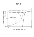
- profile of the characteristic curve changes sharply at the pinch-off rather than the conventional GaN-HEMT having no undoped In x1 Al 1-x1 N layer 4.
- a maximum value of the drain-source current I ds of the present embodiment is increased by 30 % compared to the conventional GaN-HEMT.
- FIG. 4 shows a temperature characteristic data of which temperature characteristic depend on the off current in the first embodiment of the present invention when the gate voltage is selected to -1 V.
- the off current is increased at a high temperature in the conventional technique, but an increase of the off current can be suppressed in the present invention.
- FIGS. 5A and 5B are sectional views showing a compound semiconductor device according to a second embodiment of the present invention and steps of forming the same.
- the AlN layer 2 of 0.3 ⁇ m thickness and the undoped GaN layer 3 of 2.5 ⁇ m thickness are formed as the buffer layer on the single crystal SiC substrate 1.
- an undoped In x2 Al 1-x2 N layer 14 whose In composition ratio x2 is changed in the thickness direction and whose thickness is 20 nm, the undoped GaN channel layer 5 of 100 nm thickness, the undoped Al y1 Ga 1-y1 N layer 6 of 5 nm thickness, the n-type Al y1 Ga 1-y1 N layer 7 of 20 nm thickness, and the n-type GaN layer 8 of 7 nm thickness are formed sequentially on the undoped GaN layer 3.
- a composition ratio y1 of the Al y1 Ga 1-y1 N layers 6, 7 is set to 0.33, for example.
- a composition ratio x2 of the undoped In x2 Al 1-x2 N layer 14 is changed to reduce toward the upper side such that a lowermost layer of the undoped In x2 Al 1-x2 N layer 14 is 0.2 and an uppermost layer thereof is 0.15, for example.
- a continuous change of the composition is employed herein, but a stepwise change may also be employed.
- Si is doped in the n-type Al y1 Ga 1-y1 N layer 7 at a concentration of 4 ⁇ 10 18 cm -3 , for example. Also, Si is doped in the n-type GaN layer 8 at a concentration of 5 ⁇ 10 18 cm -3 , for example.
- Al, Ga, In, Al, N, and dopants constituting respective layers are supplied by using the same materials as those shown in the first embodiment.
- the silicon nitride film 9 is formed as a protection film on the n-type GaN layer 8 by the plasma CVD method to have a thickness of about 40 nm, for example.
- the silicon nitride film 9 is patterned by the photolithography method.
- the source opening portion 9s and the drain opening portion 9d are formed in the source region and the drain region respectively.
- the n-type GaN layer 8 is etched through the source opening portion 9s and the drain opening portion 9d by the similar method to the first embodiment.
- the n-type Al y1 Ga 1-y1 N layer 7 is exposed from the source opening portion 9s and the drain opening portion 9d.
- the source electrode 10s and the drain electrode 10d which form ohmic-contacts to the n-type Al y1 Ga 1-y1 N layer 7 are formed in the source opening portion 9s and the drain opening portion 9d by the similar method to the first embodiment.
- the gate opening portion 9g is formed between the source opening portion 9s and the drain opening portion 9d by the similar method to the first embodiment. Then, the gate electrode 11 which forms Schottky-contact to the n-type GaN layer 8 through the gate opening portion 9g is formed in the gate opening portion 9g.
- the gate electrode 11 is formed of a two-layered structure consisting of a Ni layer and an Au layer, for example, and is formed in the same size as the first embodiment. Also, each of the source electrode 10s and the drain electrode 10d is formed of a two-layered structure consisting of a Ti layer and an Al layer.
- the element isolation recess is formed by etching the periphery of the element by using a mask.
- a two-dimensional electron gas of high-concentration carriers is generated by piezo polarization at the heterojunction interface between the undoped GaN layer 5 and the undoped Aly 1 Ga 1-y1 N layer 6.
- the heterojunction interface on the undoped GaN layer 5 serves as the channel region.
- a composition ratio x2 of a lowermost layer of the undoped In x2 Al 1-x2 N layer 14 is 0.2 and a composition ratio x2 of an uppermost layer thereof is 0.15.
- a lattice constant of the undoped In x2 Al 1-x2 N layer 14 is larger than that of the underlying undoped GaN layer 3 but smaller than that of the overlying undoped GaN layer 5. Also, the undoped In x2 Al 1-x2 N layer 14 has an energy bandgap larger than those of the underlying and overlying undoped GaN layers 3, 5.
- the lattice mismatching between the undoped In x2 Al 1-x2 N layer 14 and the overlying undoped GaN layer 5.
- the lattice constant of the undoped GaN layer 5 is larger than that of the undoped In x2 Al 1-x2 N layer 14.
- a two-dimensional electron gas is not generated in a lower layer portion of the undoped GaN layer 5 acting as the channel region, but the underlying undoped In x2 Al 1-x2 N layer 14 acts as the barrier.
- the electrons being accelerated in the channel region and having a high energy cannot diffuse into the buffer layer, so that it becomes easy to control a drain-source current I ds by a gate voltage to off.
- a profile of the characteristic curve changed sharply at the pinch-off rather than the conventional GaN-HEMT having no undoped In x2 Al 1-x2 N layer.
- a maximum value of the drain-source current I ds of the device in the conventional technique is larger than that of the device of the present embodiment, but the device of the present embodiment can get the better pinch-off characteristic than the GaN-HEMT according to the first embodiment.
- FIG. 8A is a sectional view showing a semiconductor device according to a third embodiment of the present invention
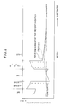
- FIG. 8B is a diagram showing a relationship between a lattice constant and an energy band gap of a nitride compound semiconductor.
- the silicon nitride film 9 is formed as a protection film on the n-type GaN layer 8 to have a thickness of about 40 nm, for example.
- the source opening portion 9s and the drain opening portion 9d are formed in the silicon nitride film 9 and the n-type GaN layer 8 at an interval. Then, the source electrode 10s and the drain electrode 10d both which form ohmic-contacts to the n-type Al y1 Ga 1-y1 N layer 7 are formed in the source opening portion 9s and the drain opening portion 9d respectively.
- the gate opening portion 9g is formed in the silicon nitride film 9 between the source electrode 10s and the drain electrode 10d at an interval from these electrodes. Also, the gate electrode 11 forms Schottky-contact to the n-type GaN layer 8 via the gate opening portion 9g.
- the nitride compound semiconductor in which composition ratios x, y of the constitutive elements in the undoped (In x Al 1-x ) y Ga 1-y N layer 24 formed under the undoped GaN layer 5 having the channel region are in ranges of 0 ⁇ x ⁇ 1 and 0 ⁇ y ⁇ 1 and which contains at least InN having the larger energy bandgap than GaN should be employed as the condition.
- the composition ratio x of 0.13 to 0.20 is preferable, and the composition ratio y of 0.9 to 0.95 is preferable.
- the composition ratio x should be set to such a level that a phase separation is never generated in the undoped (In x Al 1-x ) y Ga 1-y N layer 24.
- the undoped (In x Al 1-x ) y Ga 1-y N layer 24 should be set in the area that is surrounded with a broken line based on a relationship between the energy bandgap and the lattice constant shown in FIG. 8B .
- a conduction band energy band is brought into a condition that is equal to or like those shown in FIG. 2 and FIG. 6 .
- the carrier being accelerated in the channel region of the undoped GaN layer 5 moves to the barrier layer, and thus the off control of the drain-source current is facilitated.
- another nitride compound semiconductor layer may be formed between the undoped GaN layer 3 and the undoped (In x Al 1-x ) y Ga 1-y N layer 24 or between the undoped (In x Al 1-x ) y Ga 1-y N layer 24 and the undoped GaN layer 5.
- the channel region and the buffer layer are formed of the GaN layer. But a structure containing In in addition to GaN may be formed.
- the GaN-HEMT When the GaN-HEMT according to one of the first to third embodiments is employed the amplifier for the milliwave band communication, an efficiency can be enhanced.
- Such GaN-HEMT has a profound effect that contributes to a development of the milliwave band market.
- the alumina substrate, the silicon substrate, the GaN substrate, or the like may be used instead of the SiC substrate 1.
Landscapes
- Junction Field-Effect Transistors (AREA)
Applications Claiming Priority (1)
| Application Number | Priority Date | Filing Date | Title |
|---|---|---|---|
| JP2007094824A JP5292716B2 (ja) | 2007-03-30 | 2007-03-30 | 化合物半導体装置 |
Publications (3)
| Publication Number | Publication Date |
|---|---|
| EP1976016A2 true EP1976016A2 (de) | 2008-10-01 |
| EP1976016A3 EP1976016A3 (de) | 2010-01-20 |
| EP1976016B1 EP1976016B1 (de) | 2015-11-11 |
Family
ID=39575579
Family Applications (1)
| Application Number | Title | Priority Date | Filing Date |
|---|---|---|---|
| EP08153474.5A Ceased EP1976016B1 (de) | 2007-03-30 | 2008-03-27 | Verbundhalbleitervorrichtung |
Country Status (3)
| Country | Link |
|---|---|
| US (1) | US7795622B2 (de) |
| EP (1) | EP1976016B1 (de) |
| JP (1) | JP5292716B2 (de) |
Cited By (2)
| Publication number | Priority date | Publication date | Assignee | Title |
|---|---|---|---|---|
| CN103296079A (zh) * | 2012-02-28 | 2013-09-11 | 英飞凌科技奥地利有限公司 | 常关闭型化合物半导体隧道晶体管 |
| EP2216806B1 (de) * | 2009-02-04 | 2018-07-04 | Fujitsu Limited | Verbindungshalbleiterbauelement und Herstellungsverfahren dafür |
Families Citing this family (46)
| Publication number | Priority date | Publication date | Assignee | Title |
|---|---|---|---|---|
| US8519438B2 (en) | 2008-04-23 | 2013-08-27 | Transphorm Inc. | Enhancement mode III-N HEMTs |
| JP2010016089A (ja) * | 2008-07-02 | 2010-01-21 | Nec Electronics Corp | 電界効果トランジスタ、その製造方法、及び半導体装置 |
| US8289065B2 (en) * | 2008-09-23 | 2012-10-16 | Transphorm Inc. | Inductive load power switching circuits |
| US8330170B2 (en) * | 2008-12-05 | 2012-12-11 | Micron Technology, Inc. | Semiconductor device structures including transistors with energy barriers adjacent to transistor channels and associated methods |
| US7898004B2 (en) | 2008-12-10 | 2011-03-01 | Transphorm Inc. | Semiconductor heterostructure diodes |
| JP5562579B2 (ja) * | 2009-05-12 | 2014-07-30 | 日本碍子株式会社 | 半導体素子用エピタキシャル基板の作製方法 |
| US8742459B2 (en) * | 2009-05-14 | 2014-06-03 | Transphorm Inc. | High voltage III-nitride semiconductor devices |
| US8390000B2 (en) | 2009-08-28 | 2013-03-05 | Transphorm Inc. | Semiconductor devices with field plates |
| US8389977B2 (en) | 2009-12-10 | 2013-03-05 | Transphorm Inc. | Reverse side engineered III-nitride devices |
| US8816395B2 (en) * | 2010-05-02 | 2014-08-26 | Visic Technologies Ltd. | Field effect power transistors |
| KR101720589B1 (ko) * | 2010-10-11 | 2017-03-30 | 삼성전자주식회사 | 이 모드(E-mode) 고 전자 이동도 트랜지스터 및 그 제조방법 |
| US8742460B2 (en) | 2010-12-15 | 2014-06-03 | Transphorm Inc. | Transistors with isolation regions |
| US8643062B2 (en) | 2011-02-02 | 2014-02-04 | Transphorm Inc. | III-N device structures and methods |
| US8772842B2 (en) | 2011-03-04 | 2014-07-08 | Transphorm, Inc. | Semiconductor diodes with low reverse bias currents |
| US8716141B2 (en) | 2011-03-04 | 2014-05-06 | Transphorm Inc. | Electrode configurations for semiconductor devices |
| TWI544628B (zh) * | 2011-05-16 | 2016-08-01 | 瑞薩電子股份有限公司 | Field effect transistor and semiconductor device |
| JP2013038157A (ja) * | 2011-08-05 | 2013-02-21 | Covalent Materials Corp | 化合物半導体基板 |
| US8901604B2 (en) | 2011-09-06 | 2014-12-02 | Transphorm Inc. | Semiconductor devices with guard rings |
| US9257547B2 (en) | 2011-09-13 | 2016-02-09 | Transphorm Inc. | III-N device structures having a non-insulating substrate |
| US8598937B2 (en) | 2011-10-07 | 2013-12-03 | Transphorm Inc. | High power semiconductor electronic components with increased reliability |
| US8994035B2 (en) * | 2011-11-21 | 2015-03-31 | Sensor Electronic Technology, Inc. | Semiconductor device with low-conducting buried and/or surface layers |
| US9673285B2 (en) | 2011-11-21 | 2017-06-06 | Sensor Electronic Technology, Inc. | Semiconductor device with low-conducting buried and/or surface layers |
| US9165766B2 (en) | 2012-02-03 | 2015-10-20 | Transphorm Inc. | Buffer layer structures suited for III-nitride devices with foreign substrates |
| JP6054620B2 (ja) * | 2012-03-29 | 2016-12-27 | トランスフォーム・ジャパン株式会社 | 化合物半導体装置及びその製造方法 |
| WO2013155108A1 (en) | 2012-04-09 | 2013-10-17 | Transphorm Inc. | N-polar iii-nitride transistors |
| US9184275B2 (en) | 2012-06-27 | 2015-11-10 | Transphorm Inc. | Semiconductor devices with integrated hole collectors |
| US9608085B2 (en) * | 2012-10-01 | 2017-03-28 | Cree, Inc. | Predisposed high electron mobility transistor |
| US9171730B2 (en) | 2013-02-15 | 2015-10-27 | Transphorm Inc. | Electrodes for semiconductor devices and methods of forming the same |
| US9087718B2 (en) | 2013-03-13 | 2015-07-21 | Transphorm Inc. | Enhancement-mode III-nitride devices |
| US9245992B2 (en) | 2013-03-15 | 2016-01-26 | Transphorm Inc. | Carbon doping semiconductor devices |
| WO2015009514A1 (en) | 2013-07-19 | 2015-01-22 | Transphorm Inc. | Iii-nitride transistor including a p-type depleting layer |
| JP2015095605A (ja) * | 2013-11-13 | 2015-05-18 | 住友電気工業株式会社 | 半導体装置および半導体基板 |
| US9853107B2 (en) | 2014-03-28 | 2017-12-26 | Intel Corporation | Selective epitaxially grown III-V materials based devices |
| US9318593B2 (en) | 2014-07-21 | 2016-04-19 | Transphorm Inc. | Forming enhancement mode III-nitride devices |
| US9620598B2 (en) * | 2014-08-05 | 2017-04-11 | Semiconductor Components Industries, Llc | Electronic device including a channel layer including gallium nitride |
| US9536966B2 (en) | 2014-12-16 | 2017-01-03 | Transphorm Inc. | Gate structures for III-N devices |
| US9536967B2 (en) | 2014-12-16 | 2017-01-03 | Transphorm Inc. | Recessed ohmic contacts in a III-N device |
| JP6084254B2 (ja) * | 2015-06-03 | 2017-02-22 | クアーズテック株式会社 | 化合物半導体基板 |
| CN108604597B (zh) | 2016-01-15 | 2021-09-17 | 创世舫电子有限公司 | 具有al(1-x)sixo栅极绝缘体的增强模式iii-氮化物器件 |
| WO2017210323A1 (en) | 2016-05-31 | 2017-12-07 | Transphorm Inc. | Iii-nitride devices including a graded depleting layer |
| JP6966689B2 (ja) | 2017-03-31 | 2021-11-17 | 富士通株式会社 | 窒化物半導体装置及びその製造方法 |
| JP6926798B2 (ja) * | 2017-08-04 | 2021-08-25 | 富士通株式会社 | 化合物半導体装置、化合物半導体装置の製造方法、電源装置、及び高周波増幅器 |
| CN109524460B (zh) * | 2017-09-19 | 2022-05-17 | 世界先进积体电路股份有限公司 | 高空穴移动率晶体管 |
| US10256332B1 (en) * | 2017-10-27 | 2019-04-09 | Vanguard International Semiconductor Corporation | High hole mobility transistor |
| TWI780167B (zh) * | 2018-06-26 | 2022-10-11 | 晶元光電股份有限公司 | 半導體基底以及半導體元件 |
| JP7450446B2 (ja) | 2020-04-13 | 2024-03-15 | 株式会社アドバンテスト | 半導体装置、半導体装置の製造方法、および試験装置 |
Citations (2)
| Publication number | Priority date | Publication date | Assignee | Title |
|---|---|---|---|---|
| JP2006114653A (ja) | 2004-10-14 | 2006-04-27 | Hitachi Cable Ltd | 半導体エピタキシャルウェハ及び電界効果トランジスタ |
| JP2007094824A (ja) | 2005-09-29 | 2007-04-12 | Daifuku Co Ltd | 物品搬送設備 |
Family Cites Families (8)
| Publication number | Priority date | Publication date | Assignee | Title |
|---|---|---|---|---|
| JP3393602B2 (ja) * | 2000-01-13 | 2003-04-07 | 松下電器産業株式会社 | 半導体装置 |
| EP1421626A2 (de) * | 2001-08-07 | 2004-05-26 | Jan Kuzmik | Bauelemente mit hoher elektronenbeweglichkeit |
| US7030428B2 (en) * | 2001-12-03 | 2006-04-18 | Cree, Inc. | Strain balanced nitride heterojunction transistors |
| KR100583163B1 (ko) * | 2002-08-19 | 2006-05-23 | 엘지이노텍 주식회사 | 질화물 반도체 및 그 제조방법 |
| US20050133816A1 (en) * | 2003-12-19 | 2005-06-23 | Zhaoyang Fan | III-nitride quantum-well field effect transistors |
| JP2006032524A (ja) * | 2004-07-14 | 2006-02-02 | Nippon Telegr & Teleph Corp <Ntt> | 窒化物半導体ヘテロ構造電界効果トランジスタ構造とその作製法 |
| JP4832768B2 (ja) * | 2005-02-09 | 2011-12-07 | 日本電信電話株式会社 | 半導体装置 |
| US7615774B2 (en) * | 2005-04-29 | 2009-11-10 | Cree.Inc. | Aluminum free group III-nitride based high electron mobility transistors |
-
2007
- 2007-03-30 JP JP2007094824A patent/JP5292716B2/ja not_active Expired - Fee Related
-
2008
- 2008-03-27 EP EP08153474.5A patent/EP1976016B1/de not_active Ceased
- 2008-03-31 US US12/059,708 patent/US7795622B2/en active Active
Patent Citations (2)
| Publication number | Priority date | Publication date | Assignee | Title |
|---|---|---|---|---|
| JP2006114653A (ja) | 2004-10-14 | 2006-04-27 | Hitachi Cable Ltd | 半導体エピタキシャルウェハ及び電界効果トランジスタ |
| JP2007094824A (ja) | 2005-09-29 | 2007-04-12 | Daifuku Co Ltd | 物品搬送設備 |
Cited By (3)
| Publication number | Priority date | Publication date | Assignee | Title |
|---|---|---|---|---|
| EP2216806B1 (de) * | 2009-02-04 | 2018-07-04 | Fujitsu Limited | Verbindungshalbleiterbauelement und Herstellungsverfahren dafür |
| CN103296079A (zh) * | 2012-02-28 | 2013-09-11 | 英飞凌科技奥地利有限公司 | 常关闭型化合物半导体隧道晶体管 |
| CN103296079B (zh) * | 2012-02-28 | 2016-01-20 | 英飞凌科技奥地利有限公司 | 常关闭型化合物半导体隧道晶体管 |
Also Published As
| Publication number | Publication date |
|---|---|
| EP1976016A3 (de) | 2010-01-20 |
| EP1976016B1 (de) | 2015-11-11 |
| JP2008252034A (ja) | 2008-10-16 |
| JP5292716B2 (ja) | 2013-09-18 |
| US20080237606A1 (en) | 2008-10-02 |
| US7795622B2 (en) | 2010-09-14 |
Similar Documents
| Publication | Publication Date | Title |
|---|---|---|
| EP1976016B1 (de) | Verbundhalbleitervorrichtung | |
| US20220416072A1 (en) | Nitride semiconductor device and method of manufacturing the same | |
| EP3413353B1 (de) | Im normalzustand abgeschalteter hemt-transistor mit selektiver erzeugung von 2deg-kanal und herstellungsverfahren dafür | |
| US7268375B2 (en) | Inverted nitride-based semiconductor structure | |
| KR101497725B1 (ko) | 공핍형 GaN 기반 FET를 이용하는 캐스코드 회로 | |
| KR101124937B1 (ko) | 질화물계 트랜지스터를 위한 캡층 및/또는 패시베이션층,트랜지스터 구조 및 그 제조방법 | |
| CN100429786C (zh) | 在基于氮化镓的盖帽区段上有栅接触区的氮化铝镓/氮化镓高电子迁移率晶体管及其制造方法 | |
| EP1665385B1 (de) | Transistorbauelemente mit grossem bandabstand mit feldplatten | |
| US7687828B2 (en) | Field-effect transistor | |
| JP5252800B2 (ja) | エネルギー障壁を有するへテロ接合トランジスタおよび関連する方法 | |
| JP5160791B2 (ja) | 電荷移動誘起エネルギー障壁を有する窒化物へテロ接合トランジスタおよびその製造方法 | |
| US7544963B2 (en) | Binary group III-nitride based high electron mobility transistors | |
| US8872233B2 (en) | Semiconductor structure | |
| US7714359B2 (en) | Field effect transistor having nitride semiconductor layer | |
| US7985984B2 (en) | III-nitride semiconductor field effect transistor | |
| US20110024797A1 (en) | Nitride-based semiconductor device with concave gate region | |
| JP2002359256A (ja) | 電界効果型化合物半導体装置 | |
| KR100857683B1 (ko) | 질화물 반도체 소자 및 그 제조방법 | |
| US12166118B2 (en) | High electron mobility transistors (HEMTS) including a yttrium (Y) and aluminum nitride (AIN) (YAIN) alloy layer | |
| US11699723B1 (en) | N-polar III-nitride device structures with a p-type layer | |
| HK1142996B (en) | Cascode circuit employing a depletion-mode, gan-based fet |
Legal Events
| Date | Code | Title | Description |
|---|---|---|---|
| PUAI | Public reference made under article 153(3) epc to a published international application that has entered the european phase |
Free format text: ORIGINAL CODE: 0009012 |
|
| AK | Designated contracting states |
Kind code of ref document: A2 Designated state(s): AT BE BG CH CY CZ DE DK EE ES FI FR GB GR HR HU IE IS IT LI LT LU LV MC MT NL NO PL PT RO SE SI SK TR |
|
| AX | Request for extension of the european patent |
Extension state: AL BA MK RS |
|
| PUAL | Search report despatched |
Free format text: ORIGINAL CODE: 0009013 |
|
| AK | Designated contracting states |
Kind code of ref document: A3 Designated state(s): AT BE BG CH CY CZ DE DK EE ES FI FR GB GR HR HU IE IS IT LI LT LU LV MC MT NL NO PL PT RO SE SI SK TR |
|
| AX | Request for extension of the european patent |
Extension state: AL BA MK RS |
|
| 17P | Request for examination filed |
Effective date: 20100714 |
|
| AKX | Designation fees paid |
Designated state(s): DE FR GB |
|
| 17Q | First examination report despatched |
Effective date: 20120208 |
|
| GRAP | Despatch of communication of intention to grant a patent |
Free format text: ORIGINAL CODE: EPIDOSNIGR1 |
|
| INTG | Intention to grant announced |
Effective date: 20150604 |
|
| GRAS | Grant fee paid |
Free format text: ORIGINAL CODE: EPIDOSNIGR3 |
|
| GRAA | (expected) grant |
Free format text: ORIGINAL CODE: 0009210 |
|
| AK | Designated contracting states |
Kind code of ref document: B1 Designated state(s): DE FR GB |
|
| REG | Reference to a national code |
Ref country code: GB Ref legal event code: FG4D |
|
| REG | Reference to a national code |
Ref country code: DE Ref legal event code: R096 Ref document number: 602008041078 Country of ref document: DE |
|
| REG | Reference to a national code |
Ref country code: FR Ref legal event code: PLFP Year of fee payment: 9 |
|
| REG | Reference to a national code |
Ref country code: DE Ref legal event code: R097 Ref document number: 602008041078 Country of ref document: DE |
|
| PLBE | No opposition filed within time limit |
Free format text: ORIGINAL CODE: 0009261 |
|
| STAA | Information on the status of an ep patent application or granted ep patent |
Free format text: STATUS: NO OPPOSITION FILED WITHIN TIME LIMIT |
|
| 26N | No opposition filed |
Effective date: 20160812 |
|
| REG | Reference to a national code |
Ref country code: FR Ref legal event code: PLFP Year of fee payment: 10 |
|
| REG | Reference to a national code |
Ref country code: FR Ref legal event code: PLFP Year of fee payment: 11 |
|
| PGFP | Annual fee paid to national office [announced via postgrant information from national office to epo] |
Ref country code: GB Payment date: 20220203 Year of fee payment: 15 Ref country code: DE Payment date: 20220203 Year of fee payment: 15 |
|
| PGFP | Annual fee paid to national office [announced via postgrant information from national office to epo] |
Ref country code: FR Payment date: 20220209 Year of fee payment: 15 |
|
| REG | Reference to a national code |
Ref country code: DE Ref legal event code: R119 Ref document number: 602008041078 Country of ref document: DE |
|
| GBPC | Gb: european patent ceased through non-payment of renewal fee |
Effective date: 20230327 |
|
| PG25 | Lapsed in a contracting state [announced via postgrant information from national office to epo] |
Ref country code: GB Free format text: LAPSE BECAUSE OF NON-PAYMENT OF DUE FEES Effective date: 20230327 |
|
| PG25 | Lapsed in a contracting state [announced via postgrant information from national office to epo] |
Ref country code: GB Free format text: LAPSE BECAUSE OF NON-PAYMENT OF DUE FEES Effective date: 20230327 Ref country code: FR Free format text: LAPSE BECAUSE OF NON-PAYMENT OF DUE FEES Effective date: 20230331 Ref country code: DE Free format text: LAPSE BECAUSE OF NON-PAYMENT OF DUE FEES Effective date: 20231003 |