EP1976352B1 - Method for electroconductive circuit formation - Google Patents
Method for electroconductive circuit formation Download PDFInfo
- Publication number
- EP1976352B1 EP1976352B1 EP07707217A EP07707217A EP1976352B1 EP 1976352 B1 EP1976352 B1 EP 1976352B1 EP 07707217 A EP07707217 A EP 07707217A EP 07707217 A EP07707217 A EP 07707217A EP 1976352 B1 EP1976352 B1 EP 1976352B1
- Authority
- EP
- European Patent Office
- Prior art keywords
- layer
- electroconductive
- substrate
- forming
- primary substrate
- Prior art date
- Legal status (The legal status is an assumption and is not a legal conclusion. Google has not performed a legal analysis and makes no representation as to the accuracy of the status listed.)
- Ceased
Links
- 238000000034 method Methods 0.000 title claims description 25
- 230000015572 biosynthetic process Effects 0.000 title description 2
- 150000001925 cycloalkenes Chemical class 0.000 claims abstract description 72
- 229920005989 resin Polymers 0.000 claims abstract description 58
- 239000011347 resin Substances 0.000 claims abstract description 58
- 230000000873 masking effect Effects 0.000 claims abstract description 50
- 238000007772 electroless plating Methods 0.000 claims abstract description 44
- 229920005570 flexible polymer Polymers 0.000 claims abstract description 39
- 238000002347 injection Methods 0.000 claims abstract description 11
- 239000007924 injection Substances 0.000 claims abstract description 11
- 238000007788 roughening Methods 0.000 claims abstract description 7
- 239000000758 substrate Substances 0.000 claims description 150
- 238000007747 plating Methods 0.000 claims description 76
- 238000005868 electrolysis reaction Methods 0.000 claims description 35
- 239000000126 substance Substances 0.000 claims description 27
- 238000004090 dissolution Methods 0.000 claims description 16
- 238000001746 injection moulding Methods 0.000 claims description 16
- 150000001336 alkenes Chemical class 0.000 claims description 13
- JRZJOMJEPLMPRA-UHFFFAOYSA-N olefin Natural products CCCCCCCC=C JRZJOMJEPLMPRA-UHFFFAOYSA-N 0.000 claims description 13
- 238000009736 wetting Methods 0.000 claims description 13
- 229920006026 co-polymeric resin Polymers 0.000 claims description 12
- 239000000463 material Substances 0.000 abstract description 16
- 238000005530 etching Methods 0.000 abstract description 8
- 239000010410 layer Substances 0.000 description 135
- RYGMFSIKBFXOCR-UHFFFAOYSA-N Copper Chemical compound [Cu] RYGMFSIKBFXOCR-UHFFFAOYSA-N 0.000 description 51
- 229910052802 copper Inorganic materials 0.000 description 51
- 239000010949 copper Substances 0.000 description 51
- 239000003054 catalyst Substances 0.000 description 43
- 239000007788 liquid Substances 0.000 description 24
- 229920001971 elastomer Polymers 0.000 description 20
- PIBWKRNGBLPSSY-UHFFFAOYSA-L palladium(II) chloride Chemical compound Cl[Pd]Cl PIBWKRNGBLPSSY-UHFFFAOYSA-L 0.000 description 16
- 229910052751 metal Inorganic materials 0.000 description 15
- 239000002184 metal Substances 0.000 description 15
- 239000005060 rubber Substances 0.000 description 14
- PXHVJJICTQNCMI-UHFFFAOYSA-N Nickel Chemical compound [Ni] PXHVJJICTQNCMI-UHFFFAOYSA-N 0.000 description 12
- XLYOFNOQVPJJNP-UHFFFAOYSA-N water Substances O XLYOFNOQVPJJNP-UHFFFAOYSA-N 0.000 description 12
- 239000000178 monomer Substances 0.000 description 11
- -1 heat Substances 0.000 description 9
- 229920000346 polystyrene-polyisoprene block-polystyrene Polymers 0.000 description 9
- KDLHZDBZIXYQEI-UHFFFAOYSA-N Palladium Chemical compound [Pd] KDLHZDBZIXYQEI-UHFFFAOYSA-N 0.000 description 8
- QAOWNCQODCNURD-UHFFFAOYSA-N Sulfuric acid Chemical compound OS(O)(=O)=O QAOWNCQODCNURD-UHFFFAOYSA-N 0.000 description 8
- 239000003795 chemical substances by application Substances 0.000 description 8
- 239000011258 core-shell material Substances 0.000 description 8
- 229920000642 polymer Polymers 0.000 description 8
- 238000005406 washing Methods 0.000 description 8
- 230000003628 erosive effect Effects 0.000 description 7
- PCHJSUWPFVWCPO-UHFFFAOYSA-N gold Chemical compound [Au] PCHJSUWPFVWCPO-UHFFFAOYSA-N 0.000 description 7
- 229910052737 gold Inorganic materials 0.000 description 7
- 239000010931 gold Substances 0.000 description 7
- GRYLNZFGIOXLOG-UHFFFAOYSA-N Nitric acid Chemical compound O[N+]([O-])=O GRYLNZFGIOXLOG-UHFFFAOYSA-N 0.000 description 6
- 239000000806 elastomer Substances 0.000 description 6
- 239000000203 mixture Substances 0.000 description 6
- 229910052759 nickel Inorganic materials 0.000 description 6
- 229910017604 nitric acid Inorganic materials 0.000 description 6
- 238000002791 soaking Methods 0.000 description 6
- 239000000243 solution Substances 0.000 description 6
- 239000007864 aqueous solution Substances 0.000 description 4
- 229920001577 copolymer Polymers 0.000 description 4
- 150000002500 ions Chemical class 0.000 description 4
- 238000004519 manufacturing process Methods 0.000 description 4
- 229910052763 palladium Inorganic materials 0.000 description 4
- 229920000468 styrene butadiene styrene block copolymer Polymers 0.000 description 4
- 238000003466 welding Methods 0.000 description 4
- WKBPZYKAUNRMKP-UHFFFAOYSA-N 1-[2-(2,4-dichlorophenyl)pentyl]1,2,4-triazole Chemical compound C=1C=C(Cl)C=C(Cl)C=1C(CCC)CN1C=NC=N1 WKBPZYKAUNRMKP-UHFFFAOYSA-N 0.000 description 3
- HEMHJVSKTPXQMS-UHFFFAOYSA-M Sodium hydroxide Chemical compound [OH-].[Na+] HEMHJVSKTPXQMS-UHFFFAOYSA-M 0.000 description 3
- 125000002496 methyl group Chemical group [H]C([H])([H])* 0.000 description 3
- 229920003048 styrene butadiene rubber Polymers 0.000 description 3
- 229920002554 vinyl polymer Polymers 0.000 description 3
- RNFJDJUURJAICM-UHFFFAOYSA-N 2,2,4,4,6,6-hexaphenoxy-1,3,5-triaza-2$l^{5},4$l^{5},6$l^{5}-triphosphacyclohexa-1,3,5-triene Chemical compound N=1P(OC=2C=CC=CC=2)(OC=2C=CC=CC=2)=NP(OC=2C=CC=CC=2)(OC=2C=CC=CC=2)=NP=1(OC=1C=CC=CC=1)OC1=CC=CC=C1 RNFJDJUURJAICM-UHFFFAOYSA-N 0.000 description 2
- 229920002943 EPDM rubber Polymers 0.000 description 2
- 229920000181 Ethylene propylene rubber Polymers 0.000 description 2
- WSFSSNUMVMOOMR-UHFFFAOYSA-N Formaldehyde Chemical compound O=C WSFSSNUMVMOOMR-UHFFFAOYSA-N 0.000 description 2
- VEXZGXHMUGYJMC-UHFFFAOYSA-N Hydrochloric acid Chemical compound Cl VEXZGXHMUGYJMC-UHFFFAOYSA-N 0.000 description 2
- ATJFFYVFTNAWJD-UHFFFAOYSA-N Tin Chemical compound [Sn] ATJFFYVFTNAWJD-UHFFFAOYSA-N 0.000 description 2
- WGLPBDUCMAPZCE-UHFFFAOYSA-N Trioxochromium Chemical compound O=[Cr](=O)=O WGLPBDUCMAPZCE-UHFFFAOYSA-N 0.000 description 2
- 230000003213 activating effect Effects 0.000 description 2
- 239000000654 additive Substances 0.000 description 2
- 239000000956 alloy Substances 0.000 description 2
- 229910045601 alloy Inorganic materials 0.000 description 2
- 239000003963 antioxidant agent Substances 0.000 description 2
- 230000003078 antioxidant effect Effects 0.000 description 2
- 125000003118 aryl group Chemical group 0.000 description 2
- 238000003486 chemical etching Methods 0.000 description 2
- 239000003638 chemical reducing agent Substances 0.000 description 2
- KRVSOGSZCMJSLX-UHFFFAOYSA-L chromic acid Substances O[Cr](O)(=O)=O KRVSOGSZCMJSLX-UHFFFAOYSA-L 0.000 description 2
- ZSWFCLXCOIISFI-UHFFFAOYSA-N cyclopentadiene Chemical compound C1C=CC=C1 ZSWFCLXCOIISFI-UHFFFAOYSA-N 0.000 description 2
- 230000003247 decreasing effect Effects 0.000 description 2
- 230000007812 deficiency Effects 0.000 description 2
- 230000000694 effects Effects 0.000 description 2
- 239000003063 flame retardant Substances 0.000 description 2
- AWJWCTOOIBYHON-UHFFFAOYSA-N furo[3,4-b]pyrazine-5,7-dione Chemical compound C1=CN=C2C(=O)OC(=O)C2=N1 AWJWCTOOIBYHON-UHFFFAOYSA-N 0.000 description 2
- 230000002209 hydrophobic effect Effects 0.000 description 2
- 238000010030 laminating Methods 0.000 description 2
- 239000003921 oil Substances 0.000 description 2
- 230000003287 optical effect Effects 0.000 description 2
- 239000008188 pellet Substances 0.000 description 2
- BASFCYQUMIYNBI-UHFFFAOYSA-N platinum Chemical compound [Pt] BASFCYQUMIYNBI-UHFFFAOYSA-N 0.000 description 2
- 150000003839 salts Chemical class 0.000 description 2
- 229920006132 styrene block copolymer Polymers 0.000 description 2
- 239000004094 surface-active agent Substances 0.000 description 2
- 229910052718 tin Inorganic materials 0.000 description 2
- 239000011135 tin Substances 0.000 description 2
- 229930195735 unsaturated hydrocarbon Natural products 0.000 description 2
- DMYOHQBLOZMDLP-UHFFFAOYSA-N 1-[2-(2-hydroxy-3-piperidin-1-ylpropoxy)phenyl]-3-phenylpropan-1-one Chemical compound C1CCCCN1CC(O)COC1=CC=CC=C1C(=O)CCC1=CC=CC=C1 DMYOHQBLOZMDLP-UHFFFAOYSA-N 0.000 description 1
- HECLRDQVFMWTQS-RGOKHQFPSA-N 1755-01-7 Chemical compound C1[C@H]2[C@@H]3CC=C[C@@H]3[C@@H]1C=C2 HECLRDQVFMWTQS-RGOKHQFPSA-N 0.000 description 1
- ROGIWVXWXZRRMZ-UHFFFAOYSA-N 2-methylbuta-1,3-diene;styrene Chemical class CC(=C)C=C.C=CC1=CC=CC=C1 ROGIWVXWXZRRMZ-UHFFFAOYSA-N 0.000 description 1
- VSKJLJHPAFKHBX-UHFFFAOYSA-N 2-methylbuta-1,3-diene;styrene Chemical class CC(=C)C=C.C=CC1=CC=CC=C1.C=CC1=CC=CC=C1 VSKJLJHPAFKHBX-UHFFFAOYSA-N 0.000 description 1
- VYZAMTAEIAYCRO-UHFFFAOYSA-N Chromium Chemical compound [Cr] VYZAMTAEIAYCRO-UHFFFAOYSA-N 0.000 description 1
- VGGSQFUCUMXWEO-UHFFFAOYSA-N Ethene Chemical compound C=C VGGSQFUCUMXWEO-UHFFFAOYSA-N 0.000 description 1
- 239000005977 Ethylene Substances 0.000 description 1
- 244000043261 Hevea brasiliensis Species 0.000 description 1
- 229920009204 Methacrylate-butadiene-styrene Polymers 0.000 description 1
- 239000005062 Polybutadiene Substances 0.000 description 1
- 229920002367 Polyisobutene Polymers 0.000 description 1
- BQCADISMDOOEFD-UHFFFAOYSA-N Silver Chemical compound [Ag] BQCADISMDOOEFD-UHFFFAOYSA-N 0.000 description 1
- 229920001079 Thiokol (polymer) Polymers 0.000 description 1
- 229920006311 Urethane elastomer Polymers 0.000 description 1
- 239000002253 acid Substances 0.000 description 1
- 125000004018 acid anhydride group Chemical group 0.000 description 1
- 229920000800 acrylic rubber Polymers 0.000 description 1
- 229920000122 acrylonitrile butadiene styrene Polymers 0.000 description 1
- 230000004913 activation Effects 0.000 description 1
- 238000007259 addition reaction Methods 0.000 description 1
- 230000000996 additive effect Effects 0.000 description 1
- 125000002723 alicyclic group Chemical group 0.000 description 1
- 125000000217 alkyl group Chemical group 0.000 description 1
- 125000003368 amide group Chemical group 0.000 description 1
- 101150059062 apln gene Proteins 0.000 description 1
- 229920001400 block copolymer Polymers 0.000 description 1
- FACXGONDLDSNOE-UHFFFAOYSA-N buta-1,3-diene;styrene Chemical class C=CC=C.C=CC1=CC=CC=C1.C=CC1=CC=CC=C1 FACXGONDLDSNOE-UHFFFAOYSA-N 0.000 description 1
- MTAZNLWOLGHBHU-UHFFFAOYSA-N butadiene-styrene rubber Chemical class C=CC=C.C=CC1=CC=CC=C1 MTAZNLWOLGHBHU-UHFFFAOYSA-N 0.000 description 1
- 125000003178 carboxy group Chemical group [H]OC(*)=O 0.000 description 1
- 229910052804 chromium Inorganic materials 0.000 description 1
- 239000011651 chromium Substances 0.000 description 1
- 229910017052 cobalt Inorganic materials 0.000 description 1
- 239000010941 cobalt Substances 0.000 description 1
- GUTLYIVDDKVIGB-UHFFFAOYSA-N cobalt atom Chemical compound [Co] GUTLYIVDDKVIGB-UHFFFAOYSA-N 0.000 description 1
- 239000000470 constituent Substances 0.000 description 1
- 238000007796 conventional method Methods 0.000 description 1
- 229910000365 copper sulfate Inorganic materials 0.000 description 1
- ARUVKPQLZAKDPS-UHFFFAOYSA-L copper(II) sulfate Chemical compound [Cu+2].[O-][S+2]([O-])([O-])[O-] ARUVKPQLZAKDPS-UHFFFAOYSA-L 0.000 description 1
- 229920006038 crystalline resin Polymers 0.000 description 1
- 238000000354 decomposition reaction Methods 0.000 description 1
- 230000007547 defect Effects 0.000 description 1
- 238000005238 degreasing Methods 0.000 description 1
- 150000001993 dienes Chemical class 0.000 description 1
- KPUWHANPEXNPJT-UHFFFAOYSA-N disiloxane Chemical class [SiH3]O[SiH3] KPUWHANPEXNPJT-UHFFFAOYSA-N 0.000 description 1
- 239000000428 dust Substances 0.000 description 1
- 239000008151 electrolyte solution Substances 0.000 description 1
- 229920005558 epichlorohydrin rubber Polymers 0.000 description 1
- 125000003700 epoxy group Chemical group 0.000 description 1
- 125000004185 ester group Chemical group 0.000 description 1
- 239000000945 filler Substances 0.000 description 1
- 239000003574 free electron Substances 0.000 description 1
- 239000003365 glass fiber Substances 0.000 description 1
- 229920001519 homopolymer Polymers 0.000 description 1
- 238000005984 hydrogenation reaction Methods 0.000 description 1
- 238000005286 illumination Methods 0.000 description 1
- 229910052738 indium Inorganic materials 0.000 description 1
- APFVFJFRJDLVQX-UHFFFAOYSA-N indium atom Chemical compound [In] APFVFJFRJDLVQX-UHFFFAOYSA-N 0.000 description 1
- 229920000092 linear low density polyethylene Polymers 0.000 description 1
- 239000004707 linear low-density polyethylene Substances 0.000 description 1
- 229910021645 metal ion Inorganic materials 0.000 description 1
- 229920012128 methyl methacrylate acrylonitrile butadiene styrene Polymers 0.000 description 1
- 239000011259 mixed solution Substances 0.000 description 1
- 229920003052 natural elastomer Polymers 0.000 description 1
- 229920001194 natural rubber Polymers 0.000 description 1
- 125000002347 octyl group Chemical group [H]C([*])([H])C([H])([H])C([H])([H])C([H])([H])C([H])([H])C([H])([H])C([H])([H])C([H])([H])[H] 0.000 description 1
- 238000007254 oxidation reaction Methods 0.000 description 1
- 239000000049 pigment Substances 0.000 description 1
- 239000004014 plasticizer Substances 0.000 description 1
- 229910052697 platinum Inorganic materials 0.000 description 1
- 229920001084 poly(chloroprene) Polymers 0.000 description 1
- 229920000058 polyacrylate Polymers 0.000 description 1
- 229920002857 polybutadiene Polymers 0.000 description 1
- 229920001195 polyisoprene Polymers 0.000 description 1
- 229920001021 polysulfide Polymers 0.000 description 1
- 239000005077 polysulfide Substances 0.000 description 1
- 150000008117 polysulfides Polymers 0.000 description 1
- 239000011148 porous material Substances 0.000 description 1
- 239000010734 process oil Substances 0.000 description 1
- 229920005604 random copolymer Polymers 0.000 description 1
- 229920002379 silicone rubber Polymers 0.000 description 1
- 239000004945 silicone rubber Substances 0.000 description 1
- 229910052709 silver Inorganic materials 0.000 description 1
- 239000004332 silver Substances 0.000 description 1
- 229940083608 sodium hydroxide Drugs 0.000 description 1
- 235000011121 sodium hydroxide Nutrition 0.000 description 1
- 239000007787 solid Substances 0.000 description 1
- 239000002344 surface layer Substances 0.000 description 1
- 230000003746 surface roughness Effects 0.000 description 1
- XBFJAVXCNXDMBH-UHFFFAOYSA-N tetracyclo[6.2.1.1(3,6).0(2,7)]dodec-4-ene Chemical compound C1C(C23)C=CC1C3C1CC2CC1 XBFJAVXCNXDMBH-UHFFFAOYSA-N 0.000 description 1
- 229920001169 thermoplastic Polymers 0.000 description 1
- 229920006230 thermoplastic polyester resin Polymers 0.000 description 1
- 229920005992 thermoplastic resin Polymers 0.000 description 1
- 239000004416 thermosoftening plastic Substances 0.000 description 1
Images


Classifications
-
- H—ELECTRICITY
- H05—ELECTRIC TECHNIQUES NOT OTHERWISE PROVIDED FOR
- H05K—PRINTED CIRCUITS; CASINGS OR CONSTRUCTIONAL DETAILS OF ELECTRIC APPARATUS; MANUFACTURE OF ASSEMBLAGES OF ELECTRICAL COMPONENTS
- H05K3/00—Apparatus or processes for manufacturing printed circuits
- H05K3/10—Apparatus or processes for manufacturing printed circuits in which conductive material is applied to the insulating support in such a manner as to form the desired conductive pattern
- H05K3/18—Apparatus or processes for manufacturing printed circuits in which conductive material is applied to the insulating support in such a manner as to form the desired conductive pattern using precipitation techniques to apply the conductive material
- H05K3/181—Apparatus or processes for manufacturing printed circuits in which conductive material is applied to the insulating support in such a manner as to form the desired conductive pattern using precipitation techniques to apply the conductive material by electroless plating
- H05K3/182—Apparatus or processes for manufacturing printed circuits in which conductive material is applied to the insulating support in such a manner as to form the desired conductive pattern using precipitation techniques to apply the conductive material by electroless plating characterised by the patterning method
- H05K3/184—Apparatus or processes for manufacturing printed circuits in which conductive material is applied to the insulating support in such a manner as to form the desired conductive pattern using precipitation techniques to apply the conductive material by electroless plating characterised by the patterning method using masks
-
- H—ELECTRICITY
- H05—ELECTRIC TECHNIQUES NOT OTHERWISE PROVIDED FOR
- H05K—PRINTED CIRCUITS; CASINGS OR CONSTRUCTIONAL DETAILS OF ELECTRIC APPARATUS; MANUFACTURE OF ASSEMBLAGES OF ELECTRICAL COMPONENTS
- H05K1/00—Printed circuits
- H05K1/02—Details
- H05K1/03—Use of materials for the substrate
- H05K1/0313—Organic insulating material
- H05K1/0353—Organic insulating material consisting of two or more materials, e.g. two or more polymers, polymer + filler, + reinforcement
- H05K1/0373—Organic insulating material consisting of two or more materials, e.g. two or more polymers, polymer + filler, + reinforcement containing additives, e.g. fillers
-
- H—ELECTRICITY
- H05—ELECTRIC TECHNIQUES NOT OTHERWISE PROVIDED FOR
- H05K—PRINTED CIRCUITS; CASINGS OR CONSTRUCTIONAL DETAILS OF ELECTRIC APPARATUS; MANUFACTURE OF ASSEMBLAGES OF ELECTRICAL COMPONENTS
- H05K3/00—Apparatus or processes for manufacturing printed circuits
- H05K3/10—Apparatus or processes for manufacturing printed circuits in which conductive material is applied to the insulating support in such a manner as to form the desired conductive pattern
- H05K3/18—Apparatus or processes for manufacturing printed circuits in which conductive material is applied to the insulating support in such a manner as to form the desired conductive pattern using precipitation techniques to apply the conductive material
- H05K3/181—Apparatus or processes for manufacturing printed circuits in which conductive material is applied to the insulating support in such a manner as to form the desired conductive pattern using precipitation techniques to apply the conductive material by electroless plating
- H05K3/182—Apparatus or processes for manufacturing printed circuits in which conductive material is applied to the insulating support in such a manner as to form the desired conductive pattern using precipitation techniques to apply the conductive material by electroless plating characterised by the patterning method
-
- H—ELECTRICITY
- H05—ELECTRIC TECHNIQUES NOT OTHERWISE PROVIDED FOR
- H05K—PRINTED CIRCUITS; CASINGS OR CONSTRUCTIONAL DETAILS OF ELECTRIC APPARATUS; MANUFACTURE OF ASSEMBLAGES OF ELECTRICAL COMPONENTS
- H05K2201/00—Indexing scheme relating to printed circuits covered by H05K1/00
- H05K2201/01—Dielectrics
- H05K2201/0137—Materials
- H05K2201/0158—Polyalkene or polyolefin, e.g. polyethylene [PE], polypropylene [PP]
-
- H—ELECTRICITY
- H05—ELECTRIC TECHNIQUES NOT OTHERWISE PROVIDED FOR
- H05K—PRINTED CIRCUITS; CASINGS OR CONSTRUCTIONAL DETAILS OF ELECTRIC APPARATUS; MANUFACTURE OF ASSEMBLAGES OF ELECTRICAL COMPONENTS
- H05K2201/00—Indexing scheme relating to printed circuits covered by H05K1/00
- H05K2201/02—Fillers; Particles; Fibers; Reinforcement materials
- H05K2201/0203—Fillers and particles
- H05K2201/0206—Materials
- H05K2201/0212—Resin particles
-
- H—ELECTRICITY
- H05—ELECTRIC TECHNIQUES NOT OTHERWISE PROVIDED FOR
- H05K—PRINTED CIRCUITS; CASINGS OR CONSTRUCTIONAL DETAILS OF ELECTRIC APPARATUS; MANUFACTURE OF ASSEMBLAGES OF ELECTRICAL COMPONENTS
- H05K2201/00—Indexing scheme relating to printed circuits covered by H05K1/00
- H05K2201/09—Shape and layout
- H05K2201/09009—Substrate related
- H05K2201/09118—Moulded substrate
-
- H—ELECTRICITY
- H05—ELECTRIC TECHNIQUES NOT OTHERWISE PROVIDED FOR
- H05K—PRINTED CIRCUITS; CASINGS OR CONSTRUCTIONAL DETAILS OF ELECTRIC APPARATUS; MANUFACTURE OF ASSEMBLAGES OF ELECTRICAL COMPONENTS
- H05K2201/00—Indexing scheme relating to printed circuits covered by H05K1/00
- H05K2201/09—Shape and layout
- H05K2201/09818—Shape or layout details not covered by a single group of H05K2201/09009 - H05K2201/09809
- H05K2201/09909—Special local insulating pattern, e.g. as dam around component
-
- H—ELECTRICITY
- H05—ELECTRIC TECHNIQUES NOT OTHERWISE PROVIDED FOR
- H05K—PRINTED CIRCUITS; CASINGS OR CONSTRUCTIONAL DETAILS OF ELECTRIC APPARATUS; MANUFACTURE OF ASSEMBLAGES OF ELECTRICAL COMPONENTS
- H05K2203/00—Indexing scheme relating to apparatus or processes for manufacturing printed circuits covered by H05K3/00
- H05K2203/07—Treatments involving liquids, e.g. plating, rinsing
- H05K2203/0756—Uses of liquids, e.g. rinsing, coating, dissolving
- H05K2203/0773—Dissolving the filler without dissolving the matrix material; Dissolving the matrix material without dissolving the filler
-
- H—ELECTRICITY
- H05—ELECTRIC TECHNIQUES NOT OTHERWISE PROVIDED FOR
- H05K—PRINTED CIRCUITS; CASINGS OR CONSTRUCTIONAL DETAILS OF ELECTRIC APPARATUS; MANUFACTURE OF ASSEMBLAGES OF ELECTRICAL COMPONENTS
- H05K3/00—Apparatus or processes for manufacturing printed circuits
- H05K3/38—Improvement of the adhesion between the insulating substrate and the metal
- H05K3/381—Improvement of the adhesion between the insulating substrate and the metal by special treatment of the substrate
Definitions
- the present invention relates to a method for forming an electroconductive circuit by electroless plating on the surface of a substrate which is injection-molded of a cycloolefin resin. Specifically, it relates to a method for forming an electroconductive circuit which does not require imparting polarity (also referred to as wetting) in its step of electroless plating.
- a substrate is formed by injection-molding cycloolefin resin that is a non-crystalline resin containing a flexible polymer such as a rubber elastomer, etc..
- the substrate is masked by injection molding a thermoplastic polyester resin on the surface of the substrate so that a portion on which an electroconductive circuit is to be formed is not masked.
- the thus-masked substrate is then soaked in an etching solution to roughen the surfaces of the substrate and the masking material.
- a catalyst acting as a catalyst nucleus for electroless plating is added to the roughened surface of the substrate and the masking material.
- the cycloolefin resin itself has etching resistance, as the flexible polymer such as a rubber elastomer, etc. contained in the cycloolefin resin is dissolved by the etching solution, the non-masked portion of the surface of the substrate is also roughened.
- the masking material covering the surface of the substrate is removed, whereby a portion of the surface of the substrate is formed, which is roughened and provided with catalyst and on which electroconductive circuit is to be formed.
- the substrate is wholly soaked in an electroless plating liquid, whereby an electroconductive circuit can be formed on the portion on of the surface of the substrate where an electroconductive circuit is to be formed.
- the portion of the substrate where the masking material has been removed is not subjected to roughening and catalyst adding that are required for electroless plating, layers of plating are not formed thereon. Therefore, insulating property of the electroconductive circuit can be secured.
- Patent Document 1 provides a circuit substrate having low dielectric loss in high frequency region and excellent durability by using a cycloolefin resin having low dissipation factor to high-frequency signal and resistance to chemicals, heat, and water, etc. as a material for substrate for electroconductive circuit.
- this means had many problems to be improved.
- the mask of thermoplastic resin is also roughened by etching and provided with catalyst, an electroless plating layer is also formed on the mask.
- the mask In order to selectively form an electroless plating layer only on a portion of the substrate on which an electroconductive circuit is to be formed, the mask must be removed before or after electroless plating. Therefore, a step and equipment for removing the mask is required, which leads to increases of costs and production time.
- the layer tobe plated also has lowdissipation factor to high-frequency signal and resistance to chemicals, heat, and water, etc., as the substrate does. Furthermore, it is also desirable to improve compatibility of the layer to be plated with the substrate to strengthen the tight adhesion between the layer and the substrate.
- the surface on which the catalyst is to be imparted must have polar groups (hydrophilicity) that attract catalyst ion.
- a step for imparting polarity by using a surface-active agent, etc. wetting
- electroless plating is to form a plating layer of a single metal such as copper, nickel and gold, and it cannot form a plating layer of alloy. Therefore, where electroless plating is used solely, durability against contact pressure by a switch, etc., becomes insufficient, and welding, etc. of a contact for a connector on the electroconductive circuit becomes difficult.
- the first object of the present invention is to eliminate necessity of removal of the mask formed on the substrate.
- the second object thereof is to provide low dissipation factor to high-frequency signal and resistance to chemicals, heat, and water, etc. for both the substrate and mask.
- the third object thereof is to further improve compatibility of the mask material with the substrate to strengthen the tight adhesion between them.
- the fourth object thereof is to omit the step of providing polarity (wetting) to impart a catalyst for electroless plating.
- the fifth object thereof is to form an electroconductive circuit having improved durability and welding property.
- the present inventor has done intensive studies. As a result, the inventor has found that the above-mentioned problems can be solved at once by such a way that cycloolefin resin is used as the material for both the substrate and the mask selectively covering the surface of the substrate, and besides that either the substrate or the mask is mixed with flexible polymer.
- cycloolefin resin includes cycloolefin resin homopolymer and cycloolefin copolymer resin in which cycloolefin resin is copolymerized with linear olefin.
- both of them have low dissipation factor to high-frequency signal and resistance to chemicals, heat, and water, etc.
- those resins for both the substrate and the mask (masking layer) rather than only for the substrate, a circuit substrate having lower dielectric loss at the high-frequency region and better durability can be formed, as compared to the case where cycloolefin resin is used only for the substrate.
- their compatibility can be improved, which allows stronger tight adhesion between them.
- the cycloolefin resin itself has excellent etching resistance, it is not roughened by chemical etching and does not have polar groups (hydrophilicity) that attract catalyst ion. Therefore, the catalyst is not adsorbed on the surface.
- the flexible polymer is dissolved by chemical etching, whereby the surface can be readily roughened.
- the roughened surface itself has polar groups (hydrophilicity) that attract catalyst ion, a step for providing polarity (wetting) prior to addition of a catalyst is not necessary. Therefore, an electroconductive circuit can be readily formed in extremely easy steps, by electroless plating, only on the portion of the cycloolefin resin mixed with flexible polymer.
- the method for forming an electroconductive circuit comprises a first step for forming a primary substrate by injection molding cycloolefin resin mixed with flexible polymer; a second step for forming a secondary substrate by injection molding a masking layer a third step for roughening the portion not covered with the masking layer; and a fourth step for forming an electroconductive layer by electroless plating on the roughened portion, characterized in that the masking layer is formed, of cycloolefin resin not mixed with flexible polymer, which has compatibility with the primary substrate, to cover the surface of the primary substrate other than a portion thereof on which an electroconductive layer of a predetermined circuit pattern is to be formed; wherein a step for providing polarity (wetting) is omitted in the fourth step.
- a primary substrate is formed of cycloolefin resin not mixed with flexible polymer, and a layer to be plated is formed on the surface of the primary substrate by injection molding cycloolefin resin mixed with flexible polymer.
- an electroless plating layer can be selectively formed only on the surface of the layer to be plated, and the layer can possess similar properties to those mentioned above.
- the method for forming an electroconductive circuit comprises a first step for forming a primary substrate by injection molding cycloolefin resin not mixed with flexible polymer; a second step for forming a secondary substrate by injection molding a masking layer a third step for roughening the surface of the masking layer to be plated; and a fourth step for forming an electroconductive layer by electroless plating on the roughened portion, characterized in that the masking layer is formed of cycloolefin resin mixed with flexible polymer, which has compatibility with the primary substrate, on a portion of the surface of the primary substrate on which an electroconductive layer of a predetermined circuit pattern is to be formed; wherein a step for providing polarity (wetting) is omitted in the fourth step.
- the above-mentioned primary substrate has a through-hole, and that a portion of the layer to be plated is injectionmolded onto the both surfaces (sides) of the primary substrate via the through-hole.
- this structure for example, in covering the both surfaces (sides) of the primary substrate with layers to be plated, it is sufficient to fill the cycloolefin resin into a mold from only one surface (side) of the primary substrate, whereby the form of the mold, etc. can be simplified.
- the method so as to include a fifth step for forming an electrolysis plating on the electroconductive layer after the fourth step for forming the electroconductive layer, and a sixth step for removing residues of non-electroconductive deposit which is left on the surface of the cycloolefin resin not mixed with flexible polymer by chemical dissolution.
- a fifth step for forming an electrolysis plating on the electroconductive layer after the fourth step for forming the electroconductive layer, and a sixth step for removing residues of non-electroconductive deposit which is left on the surface of the cycloolefin resin not mixed with flexible polymer by chemical dissolution.
- cycloolefin resin is a cycloolefin copolymer resin comprising cycloolefin resin and linear olefin. Since cycloolefin copolymer resin not mixed with flexible polymer is transparent, light can readily pass therethrough. Therefore, when cycloolefin copolymer resin not mixed with flexible polymer is used for such as primary substrate, an electroconductive circuit having multiple functions such as light illumination, light conduction, and optical functions of lenses can be formed.
- the "flexible polymer” refers to a material that dissolves in an etchant, and examples thereof include, for example, natural rubber, polybutadiene, polyisoprene, polyisobutylene, neoprene, polysulfide rubber, Thiokol rubber, acrylic rubber, urethane rubber, silicone rubber, epichlorohydrin rubber, styrene-butadiene block copolymer, hydrogenated styrene-butadiene block copolymer (SEB), styrene-butadiene-styrene block copolymer (SBS), hydrogenated styrene-butadiene-styrene block copolymer (SEBS), styrene-isoprene block copolymer, hydrogenated styrene-isoprene block copolymer (SEP), styrene-isoprene-styrene block copolymer (SIS
- cycloolefin resin include, for example, non-crystalline polymers such as addition polymer of cycloolefin monomer and ethylene, addition polymer of cycloolefin monomer, ring-opened polymer of cycloolefin monomer and hydrogenated product thereof, polymer of aromatic vinyl monomer in which the aromatic ring portion has been hydrogenated, random or block copolymer of aromatic vinyl monomer and conjugated diene monomer in which the aromatic ring portion has been hydrogenated, and polymer of alicyclic vinyl monomer.
- non-crystalline polymers such as addition polymer of cycloolefin monomer and ethylene, addition polymer of cycloolefin monomer, ring-opened polymer of cycloolefin monomer and hydrogenated product thereof, polymer of aromatic vinyl monomer in which the aromatic ring portion has been hydrogenated, random or block copolymer of aromatic vinyl monomer and conjugated diene monomer in which the aromatic ring portion has been hydrogenated, and polymer of
- the cycloolefin monomer refers to cycloolefins obtained by addition reaction of cyclopentadiene and an olefin, etc., multi-ring unsaturated hydrocarbons such as dicyclopentadiene and tetracyclododecene, etc., as well as derivatives of multi-ring unsaturated hydrocarbons such as alkyl-substituted forms thereof, and polar group-substituted forms thereof obtained by substituting a polar group such as a carboxyl group, an acid anhydride group, an epoxy group, an amide group, and an ester group, etc.
- the "primary substrate” means a component or a portion of the component, on the surface of which the "masking layer” or “layer to be plated” mentioned hereafter can be injection molded.
- the shape of the primary substrate is not limited. Furthermore, the primary substrate is used not only for forming plane circuits but also for forming solid or cubic circuits.
- the "predetermined circuit pattern” refers to a portion of the substrate on which an electroconductive circuit is to be formed by electroless plating mentioned hereafter, which shape includes not only two-dimerisional one but also three-dimensional one. Furthermore, the "predetermined circuit pattern” also includes one provided on the surface of the internal space of the primary substrate, in which an aperture of the internal space is formed on the surface of the primary substrate.
- the “electroconductive layer” refers to a metal layer that is formed by electroless plating mentioned hereafter.
- the “masking layer” refers to a cover layer that covers the portion other than the predetermined portion on the surface of the primary substrate, which finally insulates the electroconductive circuits formed on the surface of the primary substrate each other.
- the “secondary substrate” refers to whole of the primary substrate and the “masking layer” or “layer to be plated” mentioned below that has been injection molded on the surface of the primary substrate.
- the “roughening” refers to that, where the primary substrate or layer to be plated on which the above-mentioned "flexible polymer” has been mixed has been injection molded is soaked into an etchant, surface roughness is increased by defect portions formed by selectively dissolving the "flexible polymer” that has been mixed and distributed on the surface layer of the primary substrate or layer to be plated and removing the polymer.
- the “electroless plating” is a known technique, which refers to a method in which electron is discharged by oxidization decomposition of a reducing agent in a plating liquid, and the metal dissolved in the plating liquid is deposited on the surface to be plated by reduction due to the free electron.
- metal that forms an electroconductive layer by electroless plating include copper, nickel, cobalt, tin, etc.
- the “providing polarity (wetting)” refers to, as mentioned above, providing polar groups (hydrophilicity) that attract catalyst ion to the surface on which a catalyst has been imparted, by using a surfactant, etc.
- the "electrolysis plating” refers to a known technique in which an electric current is applied to an electrolyte solution including metal ion to deposit the objective metal on a plate surface.
- an electroless plating layer is used as a cathode, and the objective metal is deposited on the electroless plating layer.
- the metal for electrolysis plating include, for example, copper, nickel, chromium, tin, gold, silver, platinum, indium, oralloysincludingthesemetals.
- the "non-electroconductive deposit” refers to metal deposited by a catalyst or electroless plating, and includes, for example, initial copper plating (non-continuous film).
- cycloolefin resin refers to a polymer having an alicyclic structure synthesized using cycloolefins as a monomer in the main chain.
- Examples of the chemical structural formula are shown in Figs. 3 and 4 .
- Specific examples of the resin having the chemical structural formula shown in Fig. 3 include “ZEONEX (registered trademark)” and “ZEONOR (registered trademark)", both manufactured by Zeon Corporation, and "ARTON” manufactured by JSR Corporation, etc.
- Examples of the copolymer of a cycloolefin monomer and a linear olefin having the chemical structural formula shown in Fig. 4 include "Topas" manufactured by Ticona, and "Apel” manufactured by Mitsui Chemicals, Inc., etc.
- the cost and time for forming a circuit can be reduced.
- dissipation factor to high-frequency signal can be further decreased, and chemical resistance, heat resistance, and water resistance, etc. can be provided.
- the compatibility of the mask material with the substrate can be further improved, whereby tight adhesion property between them can be further strengthened.
- the step for providing polarity (wetting) to add a catalyst for electroless plating the cost and production time can be reduced.
- an electroconductive circuit having improved durability and welding property can be formed. Furthermore, by laminating such electrolysis plating, excess erosion of the electroconductive layer can be prevented while removing the residue, such as a catalyst, etc. remained on the portion other than the portion on which an electroconductive layer is to be formed, using chemical dissolution. Moreover, by providing a through-pore to the primary substrate, simplification, etc. of the form of a mold can be achieved. In addition, by using a cycloolefin copolymer resin in which a flexible polymer has not been mixed, for example, for the primary substrate, multifunctional articles further having optical functions can be formed.
- cycloolefin copolymer resin a cycloolefin resin consisting of a cycloolefin cyclic resin and a linear olefin
- SESP styrene-ethylene-propylene-styrene block copolymer elastomer
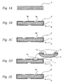
- the primary substrate 1 is then degreased by washing to remove dirt and oily components and dried.
- the secondary substrate 3 is washed, degreased (C), and dried. Then, it is soaked in an etchant so as to dissolve the SEPS constituent which is mixed and diffused in the portion 1a of the primary substrate 1 which is not covered with the masking layer 2 and on which an electroconductive layer is to be formed, as shown in Fig. 1 (D) . Thereby, the surface of the portion 1a is roughened. Since the masking layer 2 itself has etching resistance, it is not roughened even soaked in the etchant and maintains hydrophobicity.
- the etchant for example, a mixed acid solution of chromic anhydride (400 g/L) and sulfuric acid (200 mL/L) is used, and soaking is carried out at the temperature of 75°C for 60 minutes.
- the secondary substrate 3 is neutralized in alkaline aqueous solution (E) , washed and dried. Then, it is soaked into a liquid for adding a catalyst so that palladium chloride is adsorbed on the portion 1a, which is not covered with the masking layer 2 and on which an electroconductive layer is to be formed (F). Since the portion 1a of the primary substrate 1, which is not covered with the masking layer 2 and on which an electroconductive layer is to be formed, is roughened by the etchant and provided with polarity (wet) in the above-mentioned step (D), palladium chloride is adsorbed readily and tightly.
- the masking layer 2 itself is not roughened by the etchant and is hydrophobic, it does not adsorb palladium chloride as mentioned above. Therefore, palladium chloride is selectively adsorbed only on the portion 1a on which an electroconductive layer is to be formed. The adsorbed palladium chloride is then reduced by using an activating agent to form a catalyst nucleus consisting of metal palladium (G).
- the secondary substrate 3 is then washed with water and soaked into a electroless copper plating liquid to selectively form an electroconductive layer 4 of electroless copper plating on the surface of the primary substrate 1 (H).
- a general one applied toplasticmaterials may be used, for example, a solution in which 5 to 15 g/L of copper sulfate as a metal salt, 8 to 12 mL/L of formalin solution (37% by volume) as a reducing agent, 20 to 25 g/L of Rochel's salt as a complex-forming agent and 5 to 12 g/L of sodiumhydroxide as an alkaline agent have been mixed, at the temperature of 20°C, can be used.
- the electroconductive layer 4 of electroless copper plating is formed only on the portion 1a, namely, a portion of the surface of the primary substrate 1, which is not covered with the masking layer 2, on which an electroconductive layer is to be formed, and which is roughened and provided with catalyst nucleus.
- the electroconductive layer 4 is not formed on the masking layer 4, which is neither roughened nor provided with catalyst nucleus. Therefore, the electroconductive layer 4 is selectively formed only on the portion 1a of the surface of the primary substrate 1, on which an electroconductive layer of a predetermined circuit pattern is to be formed.
- the electroless copper plating liquid is then removed by washing with water, and an electrolysis copper plating 5 is formed on the surface of the electroconductive layer 4 by using itself as a cathode (I).
- an electrolysis copper plating general one may be used. If necessary, an electrolysis nickel plating layer, electrolysisgoldplating layer and the like maybe further formed on the electrolysis copper plating 5.
- the secondary substrate 3 is subjected to chemical dissolution by nitric acid liquid, etc. to remove remains of catalyst or plating (J).
- the thickness of the electrolysis copper plating 5 formed on the electroless copper plating 4 is preferably increased to some extent.
- a block-shaped primary substrate 11 is formed by injection molding cycloolefin copolymer resin, a cycloolefin resin not mixed with flexible polymer, which consists of cycloolefin resin and linear olefin.
- the primary substrate 11 is then degreased by washing to remove dirt and oil and dried. Then, as shown in Fig. 2 (B) , a layer to be plated 12 is formed on a portion of the surface of the primary substrate 11 on which an electroconductive layer of a predetermined circuit pattern by injection molding cycloolefin copolymer resin mixed with flexible polymer, which has compatibility with the primary substrate 11 and consists of cycloolefin resin and linear olefin, to form a secondary substrate 13. As mentioned above, 20% by weight of SESP is mixed and diffused as the flexible polymer.
- the secondary substrate 13 is washed, degreased (C) and dried. Then, it is soaked into etchant. Thereby, as shown in Fig. 2 (D) , since the SEPS mixed and diffused in the layer to be plated 12 is dissolved, a surface 12a of the layer to be plated 12 is roughened. Since a portion 11b of the surface of the primary substrate 11, which is not covered with the layer to be plated 12, has etching resistance, it is not roughened and maintains hydrophobicity even it is soaked in the etchant. As the etchant, those as mentioned above are used.
- the secondary substrate 13 is neutralized by using alkaline aqueous solution (E), and is washed and dried. Then, it is soaked into liquid for adding catalyst, so that palladium chloride is adsorbed on the layer to be plated 12 (F). Since the surface 12a of the layer to be plated 12 is roughened by etchant and is provided with polarity (wet) in the above-mentioned step (D), palladium chloride is readily and tightly adsorbed. On the other hand, since the primary substrate 11 itself is not roughened by etchant and is hydrophobic as mentioned above, palladium chloride is not adsorbed thereon.
- palladium chloride is selectively adsorbed only on the layer to be plated 12, which is a portion on which an electroconductive layer is to be formed.
- the adsorbed palladium chloride is then reduced using an activating agent to form a catalyst nucleus of metal palladium (G).
- the secondary substrate 13 is washed with water. Then, it is soaked into electroless copper plating liquid to selectively form a electroconductive layer 14 of electroless copper plating on the surface 12a of the layer to be plated 12 (H).
- electroless copper plating liquid those mentioned above maybe used.
- the electroconductive layer 14 of electroless copper plating is formed only on the surface 12a of the layer to be plated 12, which is roughened and is provided with catalyst nucleus.
- the layer 14 is not formed on the surface 11b on the primary substrate 11, which is neither roughened nor provided with catalyst nucleus. Therefore, the electroconductive layer 14 is formed only on the surface 12a of the layer to be plated 12 of a predetermined circuit pattern on the surface of the primary substrate 11.
- the electroless copper plating liquid is then removed by washing with water, and the electrolysis copper plating 15 is formed on the surface of the electroconductive layer 14 by using the electroconductive layer 14 itself as a cathode (I).
- the electrolysis copper plating general one may be used. If necessary, an electrolysis nickel plating, electrolysis gold plating layer, etc. may be formed on the electrolysis copper plating 15.
- the secondary substrate 13 is subjected to chemical dissolution by nitric acid liquid, etc. to remove remains of catalyst or plating (J).
- the thickness of the electrolysis copper plating 15 formed on the electroless copper plating 14 is preferably increased to some extent. Thereby, even if electrolysis plating is conducted by using copper only, since the margin thickness is prepared against erosion by chemical dissolution, the function of the electroconductive circuit is not deteriorated. Furthermore, the erosion by chemical dissolution can be prevented also by forming gold plating on the electrolysis copper plating 15.
- the nitric acid liquid, etc. is neutralized by using alkaline aqueous solution, etc. (K).
- the cycloolefin resin used for the primary substrates 1 and 11, the masking layer 2, and layer to be plated 12 may be mixed with fillers of glass fiber, bariumtitanatewhisker, etc., by which their dielectric constant can be varied, and its strength, durability, etc. can be improved. Furthermore, the cycloolefin resin may be further mixed with additives such as antiblocking agent, antioxidant, nucleus agent, antistatic, process oil, plasticizer, releasing agent, compatibilizing agent, flame retardant, flame retardant aid, pigment etc., the functional effect of each additive can be exhibited.
- additives such as antiblocking agent, antioxidant, nucleus agent, antistatic, process oil, plasticizer, releasing agent, compatibilizing agent, flame retardant, flame retardant aid, pigment etc.
- a cycloolefin resin mixed with flexible polymer was made as follows: one hundred (100) parts of "ZEONEX # RS820" manufactured by Zeon Corporation (Tg: about 190°C, hydrogenation ratio: 99.7% or more, amount of metal element: 1 ppm or less) (100 parts) was provided with thirty (30) parts of "Septon” manufactured by Kuraray Co. Ltd., number average molecular weight: 60000, Tg: at least one point at the temperature of 40°C or less, amount of metal element : 15 ppm) as a styrene-ethylene-propylene-styrene block copolymer elastomer and with point 5 (0.5) parts of a phenol-substrated antioxidant. Thereby, a pellet of a thermoplastic composition was made. Then, by injection molding the pellet at the resin temperature of 280°C a block-shaped primary substrate was formed.
- the primary substrate was then degreased by washing to remove dirt and oil and is dried.
- a masking layer which covers the surface of the primary substrate other than a portion thereof on which an electroconductive layer of a predetermined circuit pattern is to be formed, was injection molded by using cycloolefin resin ("ZEONEX #480", manufactured by Zeon Corporation) not mixed with flexible polymer, to form a secondary substrate.
- the secondary substrate is then degreased by washing, dried, and soaked in an etchant to roughen the surface of the primary substrate not covered with the above-mentioned masking layer.
- etchant a mixed solution of chromate anhydride (400 g/L) and sulfuric acid (200 mL/L) was used, and the soaking was carried out at the temperature of 75°C for 60 minutes. As a result, only the surface of the primary substrate not covered with the masking layer was roughened and wet, and the masking layer was not roughened and wet.
- the secondary substrate was then neutralized, washed and dried.
- neutralizer "Neutralizer PM50", manufactured by Shipley Far East, Ltd., was used, and the soaking was carried out at the temperature of 50°C for 3 to 5 minutes.
- the secondary substrate was then soaked into a liquid for imparting a catalyst, whereby palladium chloride was adsorbed on the surface of the primary substrate not covered with a masking layer.
- the catalyst was imparted by soaking at the temperature of 50°C for 8 to 10 minutes, using "Catapojet 44", manufactured by Shipley Far East, Ltd. As a result, it was confirmed that palladium chloride was adsorbed on the roughened surface of the primary substrate not covered with the masking layer, without further wetting.
- palladium chloride was not adsorbed on the masking layer.
- the adsorbed palladium chloride was then activated to form a catalyst nucleus of palladium metal.
- the activation was carried out by soaking at room temperature for 10 to 12 minutes using "Accelerator 19", manufactured by Shipley Far East, Ltd.
- the secondary substrate was then washed with water and soaked into electroless copper plating liquid to selectively form an electroconductive layer of electroless copper plating having a thickness of 0. 05 to 0. 3 ⁇ m on the surface of the primary substrate on which the catalyst nucleus had been formed.
- electroless copper plating liquid a mixed liquid was used which is the mixture of 72.5 % water with 12.5 % of "Copper Mix #328L", 12.5% of "Copper Mix #238A”, and 2.5 % of "Copper Mix #328C", with all of three manufactured by Shipley Far East, Ltd. , and the soaking was carried out at room temperature for 15 minutes. From the above-mentioned example, it was confirmed that an electroconductive circuit can be selectively formed by electroless copper plating only on the surface of the primary substrate, which was not covered with the masking layer and was roughened and provided with catalyst.
- cycloolefin copolymer resin consisting of cycloolefin resin and linear olefin, which is not mixed with flexible polymer
- TOPAS #RSC10001 manufactured by Polyplastics Co., Ltd. was injection molded, as mentioned above, to form a primary substrate. Dirt, dust, etc. on the surface of the primary substrate were removed by degreasing.
- a masking layer which covers the surface of the primary substrate other than a portion thereof on which an electroconductive layer of a predetermined circuit pattern is to be formed was formed by injection molding to form a secondary substrate.
- the secondary substrate was degreased by washing and was dried. Then, it is soaked in an etchant consisting of a mixture of chromic acid and sulfuric acid, whereby the surface of the primary substrate not covered with the above-mentioned masking layer was roughened.
- the chromic acid adhered on the secondary substrate was neutralized and removed by using a solution of hydrochloric acid. Palladium chloride was adhered on the roughened surface of the primary substrate as mentioned above, and the palladium chloride was reduced to form a catalyst nucleus of palladium metal. Then, the secondary substrate was provided with a standard electroless copper plating for the ABS resin.
- a primary substrate was formed by injection molding "ZEONOR #1020R", Zeon Corporation product, as a cycloolefin resin not mixed with flexible polymer. Then, a layer to be plated was injection molded on a portion of the surface of the primary substrate on which an electroconductive layer is to be formed, by using "TOPAS #RSC10001", Polyplastics Co., Ltd. product, as a cycloolefin copolymer resin consisting of cycloolefin resin and linear olefin, which is mixed with flexible polymer and has compatibility with the primary substrate, to form a secondary substrate.
- TOPAS #RSC10001 Polyplastics Co., Ltd. product
- the secondary substrate was then soaked into an etchant, a liquid for providing catalyst, and a liquid for electroless plating liquid according to the same procedure as mentioned above. As a result, it was confirmed that only the layer to be plated was roughened and was provided with the catalyst, that the surface of the primary substrate not covered with the layer to be plated was not roughened and was not provided with the catalyst, and that an electroless plating layer can be selectively formed only on the layer to be plated.
- an electroless plating layer was selectively formed on a layer to be plated that was injection-molded on the surface of the primary substrate.
- the electroless plating liquid was then removed by washing with water, and an electrolysis copper plating having a thickness of 5 to 10 ⁇ m was formed on the surface of the electroless plating layer by using the layer itself as a cathode.
- an electrolysis copper plating can be rapidly formed only on the electroless plating layer by a conventional method for electrolysis copper plating.
- the whole secondary substrate was subjected to chemical dissolution by using sulfuric acid liquid.
- the electrolysis copper plating had a sufficient margin thickness prepared against erosion by chemical dissolution and that the function of the electroconductive layer was not deteriorated. Accordingly, in a case in which remains of catalyst or plating is left on a surface of the primary substrate not covered with the layer to be plated, those remains of catalyst or plating can be sufficiently removed without causing overetching to the electrolysis copper plating.
- the method for forming an electroconductive circuit In the method for forming an electroconductive circuit according to the present invention, removal of the mask formed on the substrate is not required; the substrate and mask both have low dissipation factor to high-frequency signal; compatibility between the mask material and substrate is high; and the step for providing polarity (wetting) to impart a catalyst for electroless plating is not necessary. Therefore, said method is widely available in the industries relating to electronic devices, etc.
Landscapes
- Engineering & Computer Science (AREA)
- Microelectronics & Electronic Packaging (AREA)
- Manufacturing & Machinery (AREA)
- Manufacturing Of Printed Wiring (AREA)
- Chemically Coating (AREA)
Abstract
Applications Claiming Priority (2)
| Application Number | Priority Date | Filing Date | Title |
|---|---|---|---|
| JP2006018434A JP4478115B2 (ja) | 2006-01-27 | 2006-01-27 | 導電性回路の形成方法 |
| PCT/JP2007/050954 WO2007086359A1 (ja) | 2006-01-27 | 2007-01-23 | 導電性回路の形成方法 |
Publications (3)
| Publication Number | Publication Date |
|---|---|
| EP1976352A1 EP1976352A1 (en) | 2008-10-01 |
| EP1976352A4 EP1976352A4 (en) | 2009-12-02 |
| EP1976352B1 true EP1976352B1 (en) | 2010-09-29 |
Family
ID=38309149
Family Applications (1)
| Application Number | Title | Priority Date | Filing Date |
|---|---|---|---|
| EP07707217A Ceased EP1976352B1 (en) | 2006-01-27 | 2007-01-23 | Method for electroconductive circuit formation |
Country Status (6)
| Country | Link |
|---|---|
| US (1) | US20090000951A1 (ja) |
| EP (1) | EP1976352B1 (ja) |
| JP (1) | JP4478115B2 (ja) |
| CN (1) | CN101375649B (ja) |
| DE (1) | DE602007009482D1 (ja) |
| WO (1) | WO2007086359A1 (ja) |
Families Citing this family (7)
| Publication number | Priority date | Publication date | Assignee | Title |
|---|---|---|---|---|
| JP5332058B2 (ja) * | 2009-01-09 | 2013-11-06 | アキレス株式会社 | 成形回路部品の製造方法 |
| CN102373492A (zh) * | 2010-08-13 | 2012-03-14 | 北大方正集团有限公司 | 电路板表面进行选择性电镀的方法和电路板 |
| JP5022501B2 (ja) * | 2010-11-04 | 2012-09-12 | 株式会社日本表面処理研究所 | 成形回路部品の製造方法 |
| KR101823660B1 (ko) | 2013-08-09 | 2018-01-30 | 주식회사 엘지화학 | 전자기파의 직접 조사에 의한 도전성 패턴 형성 방법과, 도전성 패턴을 갖는 수지 구조체 |
| CN104561953A (zh) * | 2013-10-22 | 2015-04-29 | 富士康(昆山)电脑接插件有限公司 | 化学镀产品及其成型方法 |
| TWI544847B (zh) * | 2013-10-22 | 2016-08-01 | 鴻騰精密科技股份有限公司 | 化學鍍產品及其成型方法 |
| CN103874337A (zh) * | 2014-03-05 | 2014-06-18 | 东莞劲胜精密组件股份有限公司 | 非金属基材金属化方法及产品 |
Family Cites Families (12)
| Publication number | Priority date | Publication date | Assignee | Title |
|---|---|---|---|---|
| US4859571A (en) * | 1986-12-30 | 1989-08-22 | E. I. Du Pont De Nemours And Company | Embedded catalyst receptors for metallization of dielectrics |
| US5084299A (en) * | 1989-08-10 | 1992-01-28 | Microelectronics And Computer Technology Corporation | Method for patterning electroless plated metal on a polymer substrate |
| US5300208A (en) * | 1989-08-14 | 1994-04-05 | International Business Machines Corporation | Fabrication of printed circuit boards using conducting polymer |
| JPH07288374A (ja) * | 1994-04-18 | 1995-10-31 | Hitachi Cable Ltd | 射出成形回路部品の製造方法 |
| JP3498937B2 (ja) * | 1997-05-08 | 2004-02-23 | 三井化学株式会社 | 樹脂基板およびその製造方法 |
| MY139405A (en) * | 1998-09-28 | 2009-09-30 | Ibiden Co Ltd | Printed circuit board and method for its production |
| EP2053908B1 (en) * | 1999-08-12 | 2011-12-21 | Ibiden Co., Ltd. | Multilayer printed wiring board with a solder resist composition |
| JP3503546B2 (ja) * | 1999-11-01 | 2004-03-08 | 信越化学工業株式会社 | 金属パターンの形成方法 |
| JP4426690B2 (ja) * | 2000-02-28 | 2010-03-03 | 三共化成株式会社 | 立体回路基板の製造方法及び立体回路基板 |
| JP2002374066A (ja) * | 2001-06-14 | 2002-12-26 | Ibiden Co Ltd | 多層プリント配線板の製造方法 |
| JP2003115645A (ja) | 2001-10-05 | 2003-04-18 | Nippon Zeon Co Ltd | 立体回路基板 |
| WO2006085669A1 (en) * | 2005-02-08 | 2006-08-17 | Fujifilm Corporation | Metallic pattern forming method, metallic pattern obtained thereby, printed wiring board using the same, and tft wiring board using the same |
-
2006
- 2006-01-27 JP JP2006018434A patent/JP4478115B2/ja not_active Expired - Fee Related
-
2007
- 2007-01-23 CN CN2007800035901A patent/CN101375649B/zh not_active Expired - Fee Related
- 2007-01-23 US US12/087,441 patent/US20090000951A1/en not_active Abandoned
- 2007-01-23 WO PCT/JP2007/050954 patent/WO2007086359A1/ja not_active Ceased
- 2007-01-23 EP EP07707217A patent/EP1976352B1/en not_active Ceased
- 2007-01-23 DE DE602007009482T patent/DE602007009482D1/de active Active
Also Published As
| Publication number | Publication date |
|---|---|
| US20090000951A1 (en) | 2009-01-01 |
| DE602007009482D1 (de) | 2010-11-11 |
| EP1976352A4 (en) | 2009-12-02 |
| CN101375649B (zh) | 2011-03-16 |
| CN101375649A (zh) | 2009-02-25 |
| EP1976352A1 (en) | 2008-10-01 |
| JP4478115B2 (ja) | 2010-06-09 |
| WO2007086359A1 (ja) | 2007-08-02 |
| JP2007201212A (ja) | 2007-08-09 |
Similar Documents
| Publication | Publication Date | Title |
|---|---|---|
| EP1976352B1 (en) | Method for electroconductive circuit formation | |
| US8663485B2 (en) | Method of manufacturing plastic metallized three-dimensional circuit | |
| TWI328416B (en) | Multi-layer printed circuit board and method for fabricating the same | |
| JP5584676B2 (ja) | プラスチック金属化立体配線の製造方法 | |
| CN100518449C (zh) | 制备多层印制线路板的方法和多层印制线路板 | |
| KR20090079913A (ko) | 금속막이 부착된 기판의 제작 방법, 금속막이 부착된 기판, 금속 패턴 재료의 제작 방법, 금속 패턴 재료 | |
| JP3031459B2 (ja) | 立体回路基板の作製方法 | |
| JP6056760B2 (ja) | 絶縁性接着フィルム、積層体、硬化物、及び複合体 | |
| TW201800608A (zh) | 鍍敷零件之製造方法、鍍敷零件、觸媒活性抑制劑及無電解鍍敷用複合材料 | |
| KR20040111053A (ko) | 금속층 형성방법 | |
| CN103270110B (zh) | 固化性树脂组合物、固化物、表面处理固化物及层叠体 | |
| KR20160130998A (ko) | 다층 경화성 수지 필름, 프리프레그, 적층체, 경화물, 복합체 및 다층 회로 기판 | |
| KR102718930B1 (ko) | 적층체, 성형품, 도전성 패턴 및 전자 회로 | |
| JP5691977B2 (ja) | 絶縁性接着フィルム、プリプレグ、積層体、硬化物、及び複合体 | |
| JP2015174898A (ja) | 硬化性樹脂組成物、フィルム、積層フィルム、プリプレグ、積層体、硬化物、及び複合体 | |
| EP1605481A1 (en) | Metallic keypad and method for making the same | |
| JP4478086B2 (ja) | 導電性回路の形成方法 | |
| CN112740157A (zh) | 导电性部件、触摸面板传感器、触摸面板、成型体的制造方法 | |
| KR20080087622A (ko) | 무접착 양면 fccl, 및 이를 이용한 fpcb 및 그제조 방법 | |
| TWI410455B (zh) | A high-frequency electronic component material, and a high-frequency electronic component made of the same | |
| WO2003076477A1 (en) | Molding material and electrical components | |
| JP2013010887A (ja) | 樹脂組成物、フィルム、積層体、硬化物、及び複合体 | |
| KR101555014B1 (ko) | 미세배선용 인쇄회로기판 및 이의 제조방법 | |
| JP2004319918A (ja) | フレキシブルプリント配線板の製造方法及びその製造方法で得られたフレキシブルプリント配線板 | |
| CN1981566B (zh) | 制造具有通孔的印刷电路板、电子设备单元的方法以及挠性线路薄膜在这种设备单元中的应用 |
Legal Events
| Date | Code | Title | Description |
|---|---|---|---|
| PUAI | Public reference made under article 153(3) epc to a published international application that has entered the european phase |
Free format text: ORIGINAL CODE: 0009012 |
|
| 17P | Request for examination filed |
Effective date: 20080723 |
|
| AK | Designated contracting states |
Kind code of ref document: A1 Designated state(s): DE |
|
| DAX | Request for extension of the european patent (deleted) | ||
| RBV | Designated contracting states (corrected) |
Designated state(s): DE |
|
| A4 | Supplementary search report drawn up and despatched |
Effective date: 20091029 |
|
| GRAP | Despatch of communication of intention to grant a patent |
Free format text: ORIGINAL CODE: EPIDOSNIGR1 |
|
| GRAS | Grant fee paid |
Free format text: ORIGINAL CODE: EPIDOSNIGR3 |
|
| GRAA | (expected) grant |
Free format text: ORIGINAL CODE: 0009210 |
|
| AK | Designated contracting states |
Kind code of ref document: B1 Designated state(s): DE |
|
| REF | Corresponds to: |
Ref document number: 602007009482 Country of ref document: DE Date of ref document: 20101111 Kind code of ref document: P |
|
| PLBE | No opposition filed within time limit |
Free format text: ORIGINAL CODE: 0009261 |
|
| STAA | Information on the status of an ep patent application or granted ep patent |
Free format text: STATUS: NO OPPOSITION FILED WITHIN TIME LIMIT |
|
| REG | Reference to a national code |
Ref country code: DE Ref legal event code: R097 Ref document number: 602007009482 Country of ref document: DE Effective date: 20110630 |
|
| PGFP | Annual fee paid to national office [announced via postgrant information from national office to epo] |
Ref country code: DE Payment date: 20140122 Year of fee payment: 8 |
|
| REG | Reference to a national code |
Ref country code: DE Ref legal event code: R119 Ref document number: 602007009482 Country of ref document: DE |
|
| PG25 | Lapsed in a contracting state [announced via postgrant information from national office to epo] |
Ref country code: DE Free format text: LAPSE BECAUSE OF NON-PAYMENT OF DUE FEES Effective date: 20150801 |