EP1978795A1 - Verfahren zur herstellung einer leiterplatte - Google Patents
Verfahren zur herstellung einer leiterplatte Download PDFInfo
- Publication number
- EP1978795A1 EP1978795A1 EP07707506A EP07707506A EP1978795A1 EP 1978795 A1 EP1978795 A1 EP 1978795A1 EP 07707506 A EP07707506 A EP 07707506A EP 07707506 A EP07707506 A EP 07707506A EP 1978795 A1 EP1978795 A1 EP 1978795A1
- Authority
- EP
- European Patent Office
- Prior art keywords
- solder
- openings
- wiring board
- printed wiring
- connection pads
- Prior art date
- Legal status (The legal status is an assumption and is not a legal conclusion. Google has not performed a legal analysis and makes no representation as to the accuracy of the status listed.)
- Withdrawn
Links
Images




Classifications
-
- H—ELECTRICITY
- H05—ELECTRIC TECHNIQUES NOT OTHERWISE PROVIDED FOR
- H05K—PRINTED CIRCUITS; CASINGS OR CONSTRUCTIONAL DETAILS OF ELECTRIC APPARATUS; MANUFACTURE OF ASSEMBLAGES OF ELECTRICAL COMPONENTS
- H05K3/00—Apparatus or processes for manufacturing printed circuits
- H05K3/40—Forming printed elements for providing electric connections to or between printed circuits
-
- H—ELECTRICITY
- H05—ELECTRIC TECHNIQUES NOT OTHERWISE PROVIDED FOR
- H05K—PRINTED CIRCUITS; CASINGS OR CONSTRUCTIONAL DETAILS OF ELECTRIC APPARATUS; MANUFACTURE OF ASSEMBLAGES OF ELECTRICAL COMPONENTS
- H05K3/00—Apparatus or processes for manufacturing printed circuits
- H05K3/30—Assembling printed circuits with electric components, e.g. with resistors
- H05K3/32—Assembling printed circuits with electric components, e.g. with resistors electrically connecting electric components or wires to printed circuits
- H05K3/34—Assembling printed circuits with electric components, e.g. with resistors electrically connecting electric components or wires to printed circuits by soldering
- H05K3/3465—Application of solder
- H05K3/3478—Application of solder preforms; Transferring prefabricated solder patterns
-
- H—ELECTRICITY
- H10—SEMICONDUCTOR DEVICES; ELECTRIC SOLID-STATE DEVICES NOT OTHERWISE PROVIDED FOR
- H10W—GENERIC PACKAGES, INTERCONNECTIONS, CONNECTORS OR OTHER CONSTRUCTIONAL DETAILS OF DEVICES COVERED BY CLASS H10
- H10W70/00—Package substrates; Interposers; Redistribution layers [RDL]
- H10W70/01—Manufacture or treatment
- H10W70/05—Manufacture or treatment of insulating or insulated package substrates, or of interposers, or of redistribution layers
- H10W70/093—Connecting or disconnecting other interconnections thereto or therefrom, e.g. connecting bond wires or bumps
-
- H—ELECTRICITY
- H10—SEMICONDUCTOR DEVICES; ELECTRIC SOLID-STATE DEVICES NOT OTHERWISE PROVIDED FOR
- H10W—GENERIC PACKAGES, INTERCONNECTIONS, CONNECTORS OR OTHER CONSTRUCTIONAL DETAILS OF DEVICES COVERED BY CLASS H10
- H10W72/00—Interconnections or connectors in packages
- H10W72/01—Manufacture or treatment
- H10W72/011—Apparatus therefor
- H10W72/0112—Apparatus for manufacturing bump connectors
-
- H—ELECTRICITY
- H05—ELECTRIC TECHNIQUES NOT OTHERWISE PROVIDED FOR
- H05K—PRINTED CIRCUITS; CASINGS OR CONSTRUCTIONAL DETAILS OF ELECTRIC APPARATUS; MANUFACTURE OF ASSEMBLAGES OF ELECTRICAL COMPONENTS
- H05K2201/00—Indexing scheme relating to printed circuits covered by H05K1/00
- H05K2201/01—Dielectrics
- H05K2201/0183—Dielectric layers
- H05K2201/0191—Dielectric layers wherein the thickness of the dielectric plays an important role
-
- H—ELECTRICITY
- H05—ELECTRIC TECHNIQUES NOT OTHERWISE PROVIDED FOR
- H05K—PRINTED CIRCUITS; CASINGS OR CONSTRUCTIONAL DETAILS OF ELECTRIC APPARATUS; MANUFACTURE OF ASSEMBLAGES OF ELECTRICAL COMPONENTS
- H05K2203/00—Indexing scheme relating to apparatus or processes for manufacturing printed circuits covered by H05K3/00
- H05K2203/04—Soldering or other types of metallurgic bonding
- H05K2203/041—Solder preforms in the shape of solder balls
-
- H—ELECTRICITY
- H05—ELECTRIC TECHNIQUES NOT OTHERWISE PROVIDED FOR
- H05K—PRINTED CIRCUITS; CASINGS OR CONSTRUCTIONAL DETAILS OF ELECTRIC APPARATUS; MANUFACTURE OF ASSEMBLAGES OF ELECTRICAL COMPONENTS
- H05K2203/00—Indexing scheme relating to apparatus or processes for manufacturing printed circuits covered by H05K3/00
- H05K2203/04—Soldering or other types of metallurgic bonding
- H05K2203/043—Reflowing of solder coated conductors, not during connection of components, e.g. reflowing solder paste
-
- H—ELECTRICITY
- H05—ELECTRIC TECHNIQUES NOT OTHERWISE PROVIDED FOR
- H05K—PRINTED CIRCUITS; CASINGS OR CONSTRUCTIONAL DETAILS OF ELECTRIC APPARATUS; MANUFACTURE OF ASSEMBLAGES OF ELECTRICAL COMPONENTS
- H05K3/00—Apparatus or processes for manufacturing printed circuits
- H05K3/30—Assembling printed circuits with electric components, e.g. with resistors
- H05K3/32—Assembling printed circuits with electric components, e.g. with resistors electrically connecting electric components or wires to printed circuits
- H05K3/34—Assembling printed circuits with electric components, e.g. with resistors electrically connecting electric components or wires to printed circuits by soldering
- H05K3/3452—Solder masks
-
- H—ELECTRICITY
- H10—SEMICONDUCTOR DEVICES; ELECTRIC SOLID-STATE DEVICES NOT OTHERWISE PROVIDED FOR
- H10W—GENERIC PACKAGES, INTERCONNECTIONS, CONNECTORS OR OTHER CONSTRUCTIONAL DETAILS OF DEVICES COVERED BY CLASS H10
- H10W72/00—Interconnections or connectors in packages
- H10W72/01—Manufacture or treatment
- H10W72/012—Manufacture or treatment of bump connectors, dummy bumps or thermal bumps
- H10W72/01221—Manufacture or treatment of bump connectors, dummy bumps or thermal bumps using local deposition
- H10W72/01225—Manufacture or treatment of bump connectors, dummy bumps or thermal bumps using local deposition in solid form, e.g. by using a powder or by stud bumping
-
- H—ELECTRICITY
- H10—SEMICONDUCTOR DEVICES; ELECTRIC SOLID-STATE DEVICES NOT OTHERWISE PROVIDED FOR
- H10W—GENERIC PACKAGES, INTERCONNECTIONS, CONNECTORS OR OTHER CONSTRUCTIONAL DETAILS OF DEVICES COVERED BY CLASS H10
- H10W72/00—Interconnections or connectors in packages
- H10W72/071—Connecting or disconnecting
- H10W72/072—Connecting or disconnecting of bump connectors
-
- H—ELECTRICITY
- H10—SEMICONDUCTOR DEVICES; ELECTRIC SOLID-STATE DEVICES NOT OTHERWISE PROVIDED FOR
- H10W—GENERIC PACKAGES, INTERCONNECTIONS, CONNECTORS OR OTHER CONSTRUCTIONAL DETAILS OF DEVICES COVERED BY CLASS H10
- H10W72/00—Interconnections or connectors in packages
- H10W72/071—Connecting or disconnecting
- H10W72/072—Connecting or disconnecting of bump connectors
- H10W72/07231—Techniques
- H10W72/07234—Using a reflow oven
-
- H—ELECTRICITY
- H10—SEMICONDUCTOR DEVICES; ELECTRIC SOLID-STATE DEVICES NOT OTHERWISE PROVIDED FOR
- H10W—GENERIC PACKAGES, INTERCONNECTIONS, CONNECTORS OR OTHER CONSTRUCTIONAL DETAILS OF DEVICES COVERED BY CLASS H10
- H10W72/00—Interconnections or connectors in packages
- H10W72/071—Connecting or disconnecting
- H10W72/072—Connecting or disconnecting of bump connectors
- H10W72/07231—Techniques
- H10W72/07236—Soldering or alloying
-
- H—ELECTRICITY
- H10—SEMICONDUCTOR DEVICES; ELECTRIC SOLID-STATE DEVICES NOT OTHERWISE PROVIDED FOR
- H10W—GENERIC PACKAGES, INTERCONNECTIONS, CONNECTORS OR OTHER CONSTRUCTIONAL DETAILS OF DEVICES COVERED BY CLASS H10
- H10W72/00—Interconnections or connectors in packages
- H10W72/20—Bump connectors, e.g. solder bumps or copper pillars; Dummy bumps; Thermal bumps
- H10W72/241—Dispositions, e.g. layouts
-
- H—ELECTRICITY
- H10—SEMICONDUCTOR DEVICES; ELECTRIC SOLID-STATE DEVICES NOT OTHERWISE PROVIDED FOR
- H10W—GENERIC PACKAGES, INTERCONNECTIONS, CONNECTORS OR OTHER CONSTRUCTIONAL DETAILS OF DEVICES COVERED BY CLASS H10
- H10W72/00—Interconnections or connectors in packages
- H10W72/90—Bond pads, in general
-
- H—ELECTRICITY
- H10—SEMICONDUCTOR DEVICES; ELECTRIC SOLID-STATE DEVICES NOT OTHERWISE PROVIDED FOR
- H10W—GENERIC PACKAGES, INTERCONNECTIONS, CONNECTORS OR OTHER CONSTRUCTIONAL DETAILS OF DEVICES COVERED BY CLASS H10
- H10W72/00—Interconnections or connectors in packages
- H10W72/90—Bond pads, in general
- H10W72/921—Structures or relative sizes of bond pads
- H10W72/923—Bond pads having multiple stacked layers
-
- H—ELECTRICITY
- H10—SEMICONDUCTOR DEVICES; ELECTRIC SOLID-STATE DEVICES NOT OTHERWISE PROVIDED FOR
- H10W—GENERIC PACKAGES, INTERCONNECTIONS, CONNECTORS OR OTHER CONSTRUCTIONAL DETAILS OF DEVICES COVERED BY CLASS H10
- H10W72/00—Interconnections or connectors in packages
- H10W72/90—Bond pads, in general
- H10W72/941—Dispositions of bond pads
- H10W72/9415—Dispositions of bond pads relative to the surface, e.g. recessed, protruding
-
- H—ELECTRICITY
- H10—SEMICONDUCTOR DEVICES; ELECTRIC SOLID-STATE DEVICES NOT OTHERWISE PROVIDED FOR
- H10W—GENERIC PACKAGES, INTERCONNECTIONS, CONNECTORS OR OTHER CONSTRUCTIONAL DETAILS OF DEVICES COVERED BY CLASS H10
- H10W90/00—Package configurations
- H10W90/701—Package configurations characterised by the relative positions of pads or connectors relative to package parts
- H10W90/721—Package configurations characterised by the relative positions of pads or connectors relative to package parts of bump connectors
- H10W90/724—Package configurations characterised by the relative positions of pads or connectors relative to package parts of bump connectors between a chip and a stacked insulating package substrate, interposer or RDL
Definitions
- This invention pertains to a method of manufacturing a printed wiring board, in particular, relates to a method of manufacturing a printed wiring board which can suitably be used for a package substrate for mounting an IC chip.
- Solder bumps are used for an electrical connection between a package substrate and an IC chip. Solder bumps are formed with the following steps.
- solder balls end up being smaller than sand grains, and with the method of using concurrently a ball arrangement mask and a squeegee in Patent Document 1 solder balls become deformed by the squeegee, leading to the unevenness of solder balls in height resulting in lower product qualities. Namely, smaller diameters of solder balls mean lower weight ratios to the surface area, giving rise to an adsorption phenomenon of solder balls due to intermolecular force.
- solder balls susceptible to aggregation are fed while being in contact with a squeegee, solder balls are damaged resulting in portions thereof missing. When portions of solder balls are missing, it gives rise to the unevenness in height among solder bumps as described in the above since the volume of a solder bump on each of the connection pads varies.
- One of the objectives of the present invention is to provide a method of manufacturing a printed wiring board on which bumps that are high in height can with certainty be formed on the small-diameter connection pads (conductor circuits that are exposed from the solder resist layer) provided in the openings in the solder resist.
- the method of manufacturing a printed wiring board having the bumps as set forth in claim 1 comprises at least the following steps
- the metal balls having a low melting point become susceptible, when they are loaded, to becoming hung up on the upper edge faces of the solder resist openings such that they cannot on occasions be loaded in the openings. Further, when the metal balls having a low melting point are reflowed, there on occasions occurs that the connection between the solder bumps and the connection pads cannot be obtained as the metal balls having a low melting point and the connection pads are apart.
- the depth of less than 3 ⁇ m lowers the ability as a dam such that the metal having a low melting point flows out when the metal balls having a low melting point are reflowed, resulting in coming in contact with the metal having a low melting point on the adjacent connection pads such that it could create short-circuiting. And, since solder balls are susceptible to bouncing over the solder resist while being transported, etc., there are occasions that the solder balls are not loaded on the connection pads.
- the thickness of the solder resist layer is adjusted such that the metal balls having a low melting point are in contact with the connection pads as they stay loaded in the openings.
- the connection between the solder bumps and the connection pads can with certainty be obtained upon reflow since the metal balls having a low melting point loaded in the openings are in contact with the connection pads.
- the metal balls having a low melting point are gathered with the use of a mask provided with opening portions corresponding to the openings in the solder resist layer and with a cylinder member being located above said mask and the air being sucked in from said cylinder member, and the metal balls having a low melting point gathered directly below the cylinder member by the above-described cylinder member or the printed wiring board and the mask being moved relative to each other in a horizontal direction are dropped into the openings of the solder resist layer via the opening portions of the mask. Accordingly, this enables fine metal balls having a low melting point to be loaded with certainty in all the openings of the solder resist layer.
- the metal balls having a low melting point are moved while not in contact, the metal balls having a low melting point can be loaded in the openings without being damaged, unlike the case using a squeegee, allowing the height of the bumps to be uniform. Further, this enables metal balls having a low melting point to be properly placed in the openings even on a printed wiring board with a much undulated surface such as a built-up multilayer wiring board.
- Fig. 12 (A) is a structural diagram illustrating the structure of a solder ball loading apparatus pertaining to one example in accordance with the present invention, and Fig. 12 (B) an arrow directional view of the solder ball loading apparatus in Fig. 12 (A) as viewed from the side of the arrow B.
- the solder ball loading apparatus 100 comprises an XY 2 suction table 114 for positioning and holding a multilayer printed wiring board 10, a vertically-moving shaft 112 for lifting and lowering said XY 2 suction table 114, a ball arrangement mask 16 provided with openings corresponding to the connection pads of the multilayer printed wiring board, a loading cylinder (a cylinder member) 124 for guiding solder balls, a suction box 126 for supplying the loading cylinder 124 with a negative pressure, a ball removing cylinder 161 for collecting excess solder balls, a suction box 166 for supplying said ball removing cylinder 161 with a negative pressure, a ball removing suction unit 168 for holding solder balls collected, a mask clamp 144 for clamping the ball arrangement mask 16, an X-direction-moving shaft for sending the loading cylinder 124 and the ball removing cylinder 161 in the X direction, a moving-shaft support guide 142 for supporting the X-direction-moving shaft 140, an X-
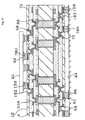
- Fig. 10 illustrates a sectional view of said multilayer printed wiring board 10
- Fig. 11 the condition in which the multilayer printed wiring board illustrated in Fig. 10 has an IC chip 90 attached thereto which is placed on a daughter board 94.
- conductive circuits 34 on the surfaces of a core substrate 30.
- the top face and the bottom face of the core substrate 30 are connected via through holes 36.
- interlayer resin insulating layers 50 having via holes 60 and conductive circuits 58 formed thereon and interlayer resin insulating layers 150 having via holes 160 and conductive circuits 158 formed thereon.
- solder resist layers 70 On said via holes 160 and conductor circuits 70 there are formed solder resist layers 70.
- the height H1 of the solder bumps 78U (the height of protrusion off the surface of the solder resist layer) is set to being about 30 ⁇ m.
- solder bumps 78D via the openings 71 of the solder resist layer 70.
- the openings of the solder resist are formed such in Fig. 10 that a portion of the conductor circuits 158 is exposed, they may be formed such that a portion of the via holes 160 and the conductor circuits 158 are included.
- solder bumps 78U on the upper face side of the multilayer printed wiring board 10 are connected to the electrode pads 92 of an IC chip 90.
- the solder bumps 78D on the lower face side are connected to the lands 96 of the daughter board 94.
- the substrate 30 having through holes 36 formed therein is, after being washed with water and dried, undergoes a blacking process with an aqueous solution containing NaOH (10g/l), NaClO 2 (40g/l), and Na 3 PO 4 (6g/l) as a blacking bath (an oxidation bath) and a reduction process with an aqueous solution containing NaOH (10g/l) and NaBH4 (6g/l) as a reduction bath to form roughened faces 36a on the side-wall conductor layers 36b of the through holes 36 and the surfaces ( Fig. 1 (D) ).
- the through holes 36 are filled with a filler 37 containing copper particles of the average particle diameter being 10 ⁇ m (a non-conductive plugging copper paste made by Tatsuta Electric Wire & Cable Co., Ltd., Product Name: DD paste) with screen printing, which is dried and hardened ( Fig. 2 (A) ).
- a coating is given with a printing method on the substrate with a mask placed thereon and provided with openings at the through hole portions to be filled in the through holes, and following the filling it is dried and hardened.
- the filler 36 which oozed out of the through holes 36 is removed by belt-sanding with the use of a #600 belt sanding paper (made by Sankyo Rikagaku Co., Ltd.), and, further, buffed to remove the flaws due to this belt-sanding to level the surfaces of substrate 30 ( Fig. 2 (B) ).
- a palladium catalyst is added to the surfaces of the substrate 30 leveled under the above-described (3) which is electroless copper-plated to form electroless copper-plated films 23 of 0.6 ⁇ m in thickness (refer to Fig. 2 (C) ).
- Electrolytic plating is conducted under the following conditions to form electrolytic copper plated films 24 of 15 ⁇ m in thickness such that an added thickness for the portions to constitute conductor circuits 34 and the portions to constitute the cover plated layers (through-hole lands) covering the filler 37 filled in through holes 36 are formed ( Fig. 2 (D) ).
- Electrolytic plating aqueous solution Sulfuric acid 180 g/l Copper sulfate 80 g/l Additive (made by Atotec JapanProduct name: Caparacid GL) 1 ml/l
- Electrolytic plating conditions Current density 1 A/dm 2 Time 70 minutes Temperature Room temperature.
- the plated films 23, 24 and the copper foils 32 at the portions where the etching resist 25 are not formed are dissolved and removed with an etching solution having cupric chloride as the main ingredient thereof, and, further, the etching resists 25 are stripped and removed with 5% KOH to form independent conductor circuits 34 and the cover plated layers 36a covering the filler 37 (refer to Fig. 3 (A) ).
- interlayer resin insulating layer 50 On both faces of the substrate there was formed an interlayer resin insulating layer 50, after a resin film for interlayer resin insulating layer (made by Ajinomoto Co., Inc. :Product Name: ABF-45SH) 50 ⁇ being slightly larger than the substrate being placed on the substrate and preliminarily pressure-bonded under the conditions of the pressure being 0.45 MPa, the temperature being 80°C, and the pressure-bonding time being 10 seconds and sheared, by being laminated with the use of a vacuum laminator by the following method ( Fig. 3 (C) ).
- the resin film for interlayer resin insulating layer was fully pressure-bonded under the conditions of the degree of vacuum being 67 Pa, the pressure being 0.47 MPa, the temperature being 85°C, and the pressure-bonding time being 60 seconds and subsequently thermoset at 170°C for 40 minutes.
- openings for via holes 51 were formed in the interlayer resin insulating layers 50 with a CO2 gas laser at the wavelength of 10.4 ⁇ m under the conditions of the beam diameter of 4.00 mm, a top hat mode, the pulse width of 3 to 30 pm, and 1 to 3 shots ( Fig. 3 (D) ).
- the above-treated substrate was immersed in a neutralizing solution (made by Shipley Company, LLC) and then washed with water. Further, to the surfaces of said substrate which have been roughened (roughening depth being 3 ⁇ m) a palladium catalyst was added such that the catalyst nucleus was adhered to the surfaces of the interlayer resin insulating layers and the inner wall surfaces of the openings for via holes. Namely, the above-described substrate was immersed in a catalyst solution containing palladium chloride (PbCl 2 ) and stannous chloride (SnCl 2 ) to allow palladium metal to deposit such to provide the catalyst.
- PbCl 2 palladium chloride
- SnCl 2 stannous chloride
- the substrate provided with the catalyst was immersed in a electroless copper plating aqueous solution (Thrucup PEA) made by Uemura Industries Co., Ltd. to form an electroless copper plated films of 0.3 to 3.0 ⁇ m in thickness over the entire roughened surfaces to obtain a substrate wherein elenctroless copper plated films were formed on the surfaces of the interlayer resin insulating layers 50 inclusive of the inner walls of the openings for via holes 51 ( Fig. 4 (B) ).
- a electroless copper plating aqueous solution made by Uemura Industries Co., Ltd.
- Electrolytic plating solution Sulfuric acid 2.24 mol/l Copper sulfate 0.26 mol/l Additive 19.5 mol/l (made by Atotec Japan, Product Name: Caparacid GL)
- Electrolytic plating conditions Current density 1 A/dm 2 Time 70 minutes Temperature 22 ⁇ 2°C
- the same processing as in the above-described (4) was conducted to from roughened faces 58a on the surfaces of the conductor circuits 58 and via holes 60.
- the thickness of the lower layer conductor circuit 58 was 15 ⁇ m ( Fig. 5(A) ). Except, the lower layer conductor circuit may be formed as having the thickness over the range of 5 to 25 ⁇ m.
- solder resist layers were hardened by heat processes under the conditions of for one hour at 80°C, for one hour at 100°C, for one hour at 120°C, and for three hours at 150°C each to form solder resist pattern layers of 30 ⁇ m in thickness having openings 71.
- the substrate was immersed in an electroless gold plating solution containing potassium gold cyanide (7.6 ⁇ 10 -3 mol/l), ammonium chloride (1.9 ⁇ 10 -1 mol/l), sodium citrate (1.2 ⁇ 10 -1 mol/l), and sodium hypophosphite (1.7 ⁇ 10 -1 mol/l) under the conditions of for 7.5 minutes at 80°C to form a gold plated layer 74 of about 0.03 ⁇ m in thickness on the nickel plated layers 72 ( Fig. 6 ).
- a nickel-gold layer a single layer of tin or a precious metal (gold, silver, palladium, platinum, etc.) may be formed.
- a nickel plated layer 72 and a gold plated layer 74 were provided on the conductor circuits 158 exposed from the openings 71 to form connection pads 158P.
- the thickness of the solder resist layers 70 was, as described in the above, adjusted to 30 ⁇ m, and with the provision of about 5 ⁇ m of a nickel plated layer 72 and about 0.03 ⁇ m of a gold plated layer 74 on the conductor circuits 158 of 15 ⁇ m in thickness the depth (D2) from the upper edge of the openings 71 to the surface of the connection pads 158P (the surface of the gold plated layer 74) was set to 10 ⁇ m.
- the solder balls 77 are supplied in a specified quantity from the solder ball supply unit 122 to the side of the loading cylinder 124. In addition, they may in advance be supplied to be stored in the loading cylinder. While Sn/Pb solder balls were used for solder balls in the examples, they may be Pb-free solder balls selected from a group of Sn and Ag, Cu, In, Bi, Zn, etc.
- the loading cylinder 124 was positioned above the ball arrangement mask 16 while maintaining a predetermined clearance (for example, 0.5 to 4 times the ball diameter) to said ball arrangement mask, as illustrated in Fig. 8 (A) , and air was suctioned from the suction portion 24b such that the flow velocity at the gap between the loading cylinder and the printed wiring board is set to 5m/sec to 35m/sec to allow the solder balls 77 to gather on the ball arrangement mask 16 directly below the opening portion 124A of said loading cylinder 124.
- a predetermined clearance for example, 0.5 to 4 times the ball diameter
- the loading cylinders 124 lined up along the Y axis of the multilayer wiring board 10 as illustrated in Fig. 8 (B) and Fig. 9 (A) as well as Fig. 12(B) and Fig. 12 (A) are moved in a horizontal direction along the X axis via the X-direction moving shaft 140.
- the solder balls 77 gathered on the ball arrangement mask 16 are moved with the movement of the loading cylinders 124 such that they are dropped via the openings 16a of the ball arrangement mask 16 and loaded into the upper face openings 71 of the multilayer printed wiring board 10.
- the solder balls 77 are successively arranged on all the connection pads on the side of the multilayer printed wiring board 10.
- the excess solder balls 77 are guided by the loading cylinders 124 to the locations where there are no openings 16a on the ball arrangement mask 16 to suction out and remove them with the ball removal cylinder 161.
- solder balls on the upper face were melted by reflow at 230°C to form solder bumps 78U of about 30 ⁇ m in height (H1) out of the solder balls 77 loaded into the openings 71 on the upper face ( Fig. 9 ).
- the distance between the solder balls 77 loaded into the openings 71 and the connection pads 158P is brought closer with the adjustment of the thickness of the solder resist layer 70 such that the connection between the solder bumps 78U and the connection pads 158P is made easily obtainable upon reflow of the solder balls 77.
- solder bumps 78U and the connection pads 158P can with certainty be obtained.
- solder bumps 78D were formed on the lower face.
- an IC chip 90 is placed onto the multilayer printed wiring board 10 and the connection pads of the printed wiring board and the electrodes 92 of the IC chip 90 are connected via the solder bumps 78U. Then, it is attached to a daughter board 94 via the solder bumps 78D ( Fig. 11 ).
- the solder balls 77 are gathered by air being suctioned out of said loading cylinders 124 and the solder balls 77 gathered directly below the loading cylinders 124 are moved such that they are on the ball arrangement mask 16 by the loading cylinders 124 or the printed wiring board and the ball arrangement mask 16 being moved relative to each other and dropped into the openings 71 of the multilayer printed wiring board 10 via the openings 16a of the ball arrangement mask 16.
- the depth D2 from the upper edge of the openings 71 to the connection pads 158P is adjusted by the thickness D4 of the solder resist layer 70 such that the solder balls 77 are in contact with the connection pads 158P.
- the opening diameter is W1 (the radius W1/2) and the radius of the solder balls 77 is R
- the thickness D4 of the solder resist layer 70 is adjusted such that the depth D2 from the upper edge of the openings to the surface of the connection pads is not greater than the distance X.
- the distance X is short. It is because air in said cavity portion V needs to be evacuated out of the solder bumps to turn the solder balls 77 to solder bumps by reflow. If air present in the cavity portion V cannot be evacuated out of the solder bumps, it would result in a poor adhesion between a connection pad and a solder bump and in the occurrence of a void within a solder bump. There are occasions when a solder bump cannot be formed on a connection pad. The larger the cavity portion V is, the more likely such a glitch is to occur.
- the test results on the yield when the solder balls 77 are loaded onto 2,500 C4 connection pads with the use of a solder ball loading apparatus described above with reference to Fig. 12 as the solder resist layer thickness, the opening diameter, and the solder ball diameter are varied is shown in the table in Fig. 14 . From these results, it was learned that the depth D2 from the upper edge of the openings to the surfaces of the connection pads to be exposed is preferably no greater than 18 ⁇ m. It is thought that this is because solder balls become susceptible to getting caught at the upper edge face of the solder resist openings such that they on occasions could not be loaded in the openings when the depth X is great.
- the range of the depth D2 is preferably 3 to 18 ⁇ m.
- solder balls may be loaded by the method of picking up and loading solder bumps onto connection pads disclosed in the Japanese Laid-Open Patent Publication No. Hei 3-265150 , the Japanese Laid-Open Patent Publication No. 2000-77837 , and the Japanese Laid-Open Patent Publication No. Hei 8-20682 , etc.
Landscapes
- Engineering & Computer Science (AREA)
- Manufacturing & Machinery (AREA)
- Microelectronics & Electronic Packaging (AREA)
- Electric Connection Of Electric Components To Printed Circuits (AREA)
Applications Claiming Priority (2)
| Application Number | Priority Date | Filing Date | Title |
|---|---|---|---|
| JP2006019522 | 2006-01-27 | ||
| PCT/JP2007/051274 WO2007086509A1 (ja) | 2006-01-27 | 2007-01-26 | プリント配線板の製造方法 |
Publications (2)
| Publication Number | Publication Date |
|---|---|
| EP1978795A1 true EP1978795A1 (de) | 2008-10-08 |
| EP1978795A4 EP1978795A4 (de) | 2012-10-31 |
Family
ID=38309295
Family Applications (1)
| Application Number | Title | Priority Date | Filing Date |
|---|---|---|---|
| EP07707506A Withdrawn EP1978795A4 (de) | 2006-01-27 | 2007-01-26 | Verfahren zur herstellung einer leiterplatte |
Country Status (7)
| Country | Link |
|---|---|
| US (1) | US8083123B2 (de) |
| EP (1) | EP1978795A4 (de) |
| JP (1) | JP4666399B2 (de) |
| KR (1) | KR100973950B1 (de) |
| CN (2) | CN101331812B (de) |
| TW (1) | TW200746964A (de) |
| WO (1) | WO2007086509A1 (de) |
Families Citing this family (15)
| Publication number | Priority date | Publication date | Assignee | Title |
|---|---|---|---|---|
| CN101854771A (zh) | 2005-06-30 | 2010-10-06 | 揖斐电株式会社 | 印刷线路板 |
| JP2009081334A (ja) * | 2007-09-27 | 2009-04-16 | Aisin Aw Co Ltd | 多層プリント配線基板及びその製造方法。 |
| KR101022942B1 (ko) * | 2008-11-12 | 2011-03-16 | 삼성전기주식회사 | 흐름 방지용 댐을 구비한 인쇄회로기판 및 그 제조방법 |
| KR101079513B1 (ko) | 2009-05-13 | 2011-11-03 | 삼성전기주식회사 | 범프 인쇄장치 및 그 제어방법 |
| US9455211B2 (en) | 2013-09-11 | 2016-09-27 | Taiwan Semiconductor Manufacturing Company, Ltd. | Integrated fan-out structure with openings in buffer layer |
| US9425121B2 (en) | 2013-09-11 | 2016-08-23 | Taiwan Semiconductor Manufacturing Company, Ltd. | Integrated fan-out structure with guiding trenches in buffer layer |
| US9508636B2 (en) | 2013-10-16 | 2016-11-29 | Intel Corporation | Integrated circuit package substrate |
| US9153550B2 (en) * | 2013-11-14 | 2015-10-06 | Taiwan Semiconductor Manufacturing Company, Ltd. | Substrate design with balanced metal and solder resist density |
| US9275955B2 (en) | 2013-12-18 | 2016-03-01 | Intel Corporation | Integrated circuit package with embedded bridge |
| JP2015231003A (ja) * | 2014-06-06 | 2015-12-21 | イビデン株式会社 | 回路基板および回路基板の製造方法 |
| WO2018155089A1 (ja) * | 2017-02-23 | 2018-08-30 | 株式会社村田製作所 | 電子部品、電子機器および電子部品の実装方法 |
| CN107318228B (zh) * | 2017-08-29 | 2019-09-06 | 郑州云海信息技术有限公司 | 一种印制电路板的制造方法及其制造装置 |
| US10695875B2 (en) * | 2018-03-19 | 2020-06-30 | Asia Vital Components Co., Ltd. | Soldering method of soldering jig |
| CN111162013B (zh) * | 2020-01-06 | 2021-08-24 | 亿芯微半导体科技(深圳)有限公司 | 一种半导体封装结构及一种半导体封装的制造方法 |
| CN111199889B (zh) * | 2020-01-10 | 2021-07-16 | 宝德照明集团有限公司 | 一种半导体封装结构及其制备方法 |
Family Cites Families (21)
| Publication number | Priority date | Publication date | Assignee | Title |
|---|---|---|---|---|
| JPH06105731B2 (ja) | 1990-03-14 | 1994-12-21 | 新日本製鐵株式▲会▼社 | バンプの転写方法及びその装置 |
| JPH0820682A (ja) | 1994-07-04 | 1996-01-23 | Mitsubishi Cable Ind Ltd | 電気絶縁性組成物 |
| JPH09326412A (ja) * | 1996-06-07 | 1997-12-16 | Tokuyama Corp | ハンダボールの取り付け方法 |
| US5921458A (en) | 1997-06-25 | 1999-07-13 | Fan; Kuang-Shu | Integrated circuit solder ball implant machine |
| EP1096650B1 (de) | 1998-07-06 | 2006-11-22 | Sanyo Electric Co., Ltd. | Schall-/ schwingungsgenerator |
| JP2000077837A (ja) | 1998-08-27 | 2000-03-14 | Ibiden Co Ltd | 半田ボール搭載装置及び搭載方法 |
| KR100866814B1 (ko) * | 1998-12-16 | 2008-11-04 | 이비덴 가부시키가이샤 | 도전성접속핀 및 패키지기판 |
| JP2001267731A (ja) | 2000-01-13 | 2001-09-28 | Hitachi Ltd | バンプ付き電子部品の製造方法および電子部品の製造方法 |
| JP4130526B2 (ja) * | 2000-11-10 | 2008-08-06 | 株式会社日立製作所 | バンプ形成方法およびその装置 |
| JP3819806B2 (ja) * | 2002-05-17 | 2006-09-13 | 富士通株式会社 | バンプ電極付き電子部品およびその製造方法 |
| JP4047251B2 (ja) * | 2003-07-31 | 2008-02-13 | 日本特殊陶業株式会社 | 配線基板および配線基板の製造方法 |
| KR100798662B1 (ko) * | 2004-08-04 | 2008-01-28 | 이비덴 가부시키가이샤 | 땜납 볼 탑재 방법 및 땜납 볼 탑재 장치 |
| JP5021472B2 (ja) * | 2005-06-30 | 2012-09-05 | イビデン株式会社 | プリント配線板の製造方法 |
| US7823762B2 (en) | 2006-09-28 | 2010-11-02 | Ibiden Co., Ltd. | Manufacturing method and manufacturing apparatus of printed wiring board |
| WO2008053833A1 (fr) * | 2006-11-03 | 2008-05-08 | Ibiden Co., Ltd. | Tableau de câblage imprimé multicouche |
| DE102007023666A1 (de) * | 2006-12-01 | 2008-06-05 | Infineon Technologies Ag | Halbleiterbaustein und Verfahren zur Herstellung eines Halbleiterbausteins |
| US7907801B2 (en) * | 2007-01-17 | 2011-03-15 | Ibiden Co., Ltd. | Optical element, package substrate and device for optical communication |
| US7972521B2 (en) * | 2007-03-12 | 2011-07-05 | Semiconductor Components Industries Llc | Method of making reliable wafer level chip scale package semiconductor devices |
| US7674987B2 (en) * | 2007-03-29 | 2010-03-09 | Ibiden Co., Ltd. | Multilayer printed circuit board |
| TWI334643B (en) * | 2007-04-11 | 2010-12-11 | Nan Ya Printed Circuit Board Corp | Solder pad and method of making the same |
| EP2157841A4 (de) * | 2008-05-30 | 2011-11-02 | Ibiden Co Ltd | Montagegerät für eine lötkugel |
-
2007
- 2007-01-23 TW TW096102452A patent/TW200746964A/zh not_active IP Right Cessation
- 2007-01-26 KR KR1020087002447A patent/KR100973950B1/ko active Active
- 2007-01-26 JP JP2007556016A patent/JP4666399B2/ja active Active
- 2007-01-26 CN CN2007800007403A patent/CN101331812B/zh not_active Expired - Fee Related
- 2007-01-26 WO PCT/JP2007/051274 patent/WO2007086509A1/ja not_active Ceased
- 2007-01-26 EP EP07707506A patent/EP1978795A4/de not_active Withdrawn
- 2007-01-26 CN CN2010106229552A patent/CN102098881A/zh active Pending
-
2008
- 2008-05-12 US US12/093,436 patent/US8083123B2/en active Active
Also Published As
| Publication number | Publication date |
|---|---|
| TWI353204B (de) | 2011-11-21 |
| KR100973950B1 (ko) | 2010-08-05 |
| EP1978795A4 (de) | 2012-10-31 |
| KR20080028467A (ko) | 2008-03-31 |
| CN101331812B (zh) | 2011-02-02 |
| US20090120680A1 (en) | 2009-05-14 |
| CN101331812A (zh) | 2008-12-24 |
| CN102098881A (zh) | 2011-06-15 |
| JP4666399B2 (ja) | 2011-04-06 |
| US8083123B2 (en) | 2011-12-27 |
| TW200746964A (en) | 2007-12-16 |
| JPWO2007086509A1 (ja) | 2009-06-25 |
| WO2007086509A1 (ja) | 2007-08-02 |
Similar Documents
| Publication | Publication Date | Title |
|---|---|---|
| EP1978795A1 (de) | Verfahren zur herstellung einer leiterplatte | |
| US9480170B2 (en) | Printed wiring board and a method of manufacturing a printed wiring board | |
| US8800143B2 (en) | Multilayer printed wiring board and manufacturing method thereof | |
| US8198546B2 (en) | Printed wiring board | |
| US8371498B2 (en) | Method for manufacturing a printed wiring board | |
| EP2012569A1 (de) | Verfahren zur montage einer lötkugel und vorrichtung zur montage einer lötkugel | |
| US7845547B2 (en) | Method for manufacturing a printed wiring board |
Legal Events
| Date | Code | Title | Description |
|---|---|---|---|
| PUAI | Public reference made under article 153(3) epc to a published international application that has entered the european phase |
Free format text: ORIGINAL CODE: 0009012 |
|
| 17P | Request for examination filed |
Effective date: 20080213 |
|
| AK | Designated contracting states |
Kind code of ref document: A1 Designated state(s): DE |
|
| RBV | Designated contracting states (corrected) |
Designated state(s): DE |
|
| DAX | Request for extension of the european patent (deleted) | ||
| A4 | Supplementary search report drawn up and despatched |
Effective date: 20120928 |
|
| RIC1 | Information provided on ipc code assigned before grant |
Ipc: H05K 3/34 20060101AFI20120924BHEP Ipc: H01L 21/60 20060101ALI20120924BHEP |
|
| STAA | Information on the status of an ep patent application or granted ep patent |
Free format text: STATUS: THE APPLICATION IS DEEMED TO BE WITHDRAWN |
|
| 18D | Application deemed to be withdrawn |
Effective date: 20130427 |