EP1986470A2 - Vorrichtung und Verfahren zur Bereitstellung einer hybriden linearen Stromquelle/Schaltstromquelle, wie etwa für eine Hochleistungs-Leuchtdioden (LED)-Rückbeleuchtung mit großem Verdunkelungsbereich - Google Patents
Vorrichtung und Verfahren zur Bereitstellung einer hybriden linearen Stromquelle/Schaltstromquelle, wie etwa für eine Hochleistungs-Leuchtdioden (LED)-Rückbeleuchtung mit großem Verdunkelungsbereich Download PDFInfo
- Publication number
- EP1986470A2 EP1986470A2 EP08251471A EP08251471A EP1986470A2 EP 1986470 A2 EP1986470 A2 EP 1986470A2 EP 08251471 A EP08251471 A EP 08251471A EP 08251471 A EP08251471 A EP 08251471A EP 1986470 A2 EP1986470 A2 EP 1986470A2
- Authority
- EP
- European Patent Office
- Prior art keywords
- power supply
- load
- current
- pwm
- linear
- Prior art date
- Legal status (The legal status is an assumption and is not a legal conclusion. Google has not performed a legal analysis and makes no representation as to the accuracy of the status listed.)
- Granted
Links
Images


Classifications
-
- H—ELECTRICITY
- H05—ELECTRIC TECHNIQUES NOT OTHERWISE PROVIDED FOR
- H05B—ELECTRIC HEATING; ELECTRIC LIGHT SOURCES NOT OTHERWISE PROVIDED FOR; CIRCUIT ARRANGEMENTS FOR ELECTRIC LIGHT SOURCES, IN GENERAL
- H05B45/00—Circuit arrangements for operating light-emitting diodes [LED]
- H05B45/20—Controlling the colour of the light
- H05B45/22—Controlling the colour of the light using optical feedback
-
- H—ELECTRICITY
- H05—ELECTRIC TECHNIQUES NOT OTHERWISE PROVIDED FOR
- H05B—ELECTRIC HEATING; ELECTRIC LIGHT SOURCES NOT OTHERWISE PROVIDED FOR; CIRCUIT ARRANGEMENTS FOR ELECTRIC LIGHT SOURCES, IN GENERAL
- H05B45/00—Circuit arrangements for operating light-emitting diodes [LED]
- H05B45/10—Controlling the intensity of the light
-
- H—ELECTRICITY
- H05—ELECTRIC TECHNIQUES NOT OTHERWISE PROVIDED FOR
- H05B—ELECTRIC HEATING; ELECTRIC LIGHT SOURCES NOT OTHERWISE PROVIDED FOR; CIRCUIT ARRANGEMENTS FOR ELECTRIC LIGHT SOURCES, IN GENERAL
- H05B45/00—Circuit arrangements for operating light-emitting diodes [LED]
- H05B45/20—Controlling the colour of the light
-
- H—ELECTRICITY
- H05—ELECTRIC TECHNIQUES NOT OTHERWISE PROVIDED FOR
- H05B—ELECTRIC HEATING; ELECTRIC LIGHT SOURCES NOT OTHERWISE PROVIDED FOR; CIRCUIT ARRANGEMENTS FOR ELECTRIC LIGHT SOURCES, IN GENERAL
- H05B45/00—Circuit arrangements for operating light-emitting diodes [LED]
- H05B45/30—Driver circuits
- H05B45/37—Converter circuits
- H05B45/3725—Switched mode power supply [SMPS]
-
- H—ELECTRICITY
- H05—ELECTRIC TECHNIQUES NOT OTHERWISE PROVIDED FOR
- H05B—ELECTRIC HEATING; ELECTRIC LIGHT SOURCES NOT OTHERWISE PROVIDED FOR; CIRCUIT ARRANGEMENTS FOR ELECTRIC LIGHT SOURCES, IN GENERAL
- H05B45/00—Circuit arrangements for operating light-emitting diodes [LED]
- H05B45/30—Driver circuits
- H05B45/395—Linear regulators
-
- H—ELECTRICITY
- H05—ELECTRIC TECHNIQUES NOT OTHERWISE PROVIDED FOR
- H05B—ELECTRIC HEATING; ELECTRIC LIGHT SOURCES NOT OTHERWISE PROVIDED FOR; CIRCUIT ARRANGEMENTS FOR ELECTRIC LIGHT SOURCES, IN GENERAL
- H05B45/00—Circuit arrangements for operating light-emitting diodes [LED]
- H05B45/40—Details of LED load circuits
- H05B45/44—Details of LED load circuits with an active control inside an LED matrix
- H05B45/46—Details of LED load circuits with an active control inside an LED matrix having LEDs disposed in parallel lines
-
- H—ELECTRICITY
- H02—GENERATION; CONVERSION OR DISTRIBUTION OF ELECTRIC POWER
- H02M—APPARATUS FOR CONVERSION BETWEEN AC AND AC, BETWEEN AC AND DC, OR BETWEEN DC AND DC, AND FOR USE WITH MAINS OR SIMILAR POWER SUPPLY SYSTEMS; CONVERSION OF DC OR AC INPUT POWER INTO SURGE OUTPUT POWER; CONTROL OR REGULATION THEREOF
- H02M1/00—Details of apparatus for conversion
- H02M1/0045—Converters combining the concepts of switch-mode regulation and linear regulation, e.g. linear pre-regulator to switching converter, linear and switching converter in parallel, same converter or same transistor operating either in linear or switching mode
-
- H—ELECTRICITY
- H02—GENERATION; CONVERSION OR DISTRIBUTION OF ELECTRIC POWER
- H02M—APPARATUS FOR CONVERSION BETWEEN AC AND AC, BETWEEN AC AND DC, OR BETWEEN DC AND DC, AND FOR USE WITH MAINS OR SIMILAR POWER SUPPLY SYSTEMS; CONVERSION OF DC OR AC INPUT POWER INTO SURGE OUTPUT POWER; CONTROL OR REGULATION THEREOF
- H02M3/00—Conversion of DC power input into DC power output
- H02M3/02—Conversion of DC power input into DC power output without intermediate conversion into AC
- H02M3/04—Conversion of DC power input into DC power output without intermediate conversion into AC by static converters
- H02M3/10—Conversion of DC power input into DC power output without intermediate conversion into AC by static converters using discharge tubes with control electrode or semiconductor devices with control electrode
- H02M3/145—Conversion of DC power input into DC power output without intermediate conversion into AC by static converters using discharge tubes with control electrode or semiconductor devices with control electrode using devices of a triode or transistor type requiring continuous application of a control signal
- H02M3/155—Conversion of DC power input into DC power output without intermediate conversion into AC by static converters using discharge tubes with control electrode or semiconductor devices with control electrode using devices of a triode or transistor type requiring continuous application of a control signal using semiconductor devices only
- H02M3/156—Conversion of DC power input into DC power output without intermediate conversion into AC by static converters using discharge tubes with control electrode or semiconductor devices with control electrode using devices of a triode or transistor type requiring continuous application of a control signal using semiconductor devices only with automatic control of output voltage or current, e.g. switching regulators
- H02M3/158—Conversion of DC power input into DC power output without intermediate conversion into AC by static converters using discharge tubes with control electrode or semiconductor devices with control electrode using devices of a triode or transistor type requiring continuous application of a control signal using semiconductor devices only with automatic control of output voltage or current, e.g. switching regulators including plural semiconductor devices as final control devices for a single load
- H02M3/1584—Conversion of DC power input into DC power output without intermediate conversion into AC by static converters using discharge tubes with control electrode or semiconductor devices with control electrode using devices of a triode or transistor type requiring continuous application of a control signal using semiconductor devices only with automatic control of output voltage or current, e.g. switching regulators including plural semiconductor devices as final control devices for a single load with a plurality of power processing stages connected in parallel
-
- Y—GENERAL TAGGING OF NEW TECHNOLOGICAL DEVELOPMENTS; GENERAL TAGGING OF CROSS-SECTIONAL TECHNOLOGIES SPANNING OVER SEVERAL SECTIONS OF THE IPC; TECHNICAL SUBJECTS COVERED BY FORMER USPC CROSS-REFERENCE ART COLLECTIONS [XRACs] AND DIGESTS
- Y02—TECHNOLOGIES OR APPLICATIONS FOR MITIGATION OR ADAPTATION AGAINST CLIMATE CHANGE
- Y02B—CLIMATE CHANGE MITIGATION TECHNOLOGIES RELATED TO BUILDINGS, e.g. HOUSING, HOUSE APPLIANCES OR RELATED END-USER APPLICATIONS
- Y02B20/00—Energy efficient lighting technologies, e.g. halogen lamps or gas discharge lamps
- Y02B20/30—Semiconductor lamps, e.g. solid state lamps [SSL] light emitting diodes [LED] or organic LED [OLED]
Definitions
- the present disclosure generally relates to a method and apparatus to drive light sources, and in particular but not exclusively, relates to a method and apparatus to dim or otherwise adjust brightness of light sources, such as light emitting diode (LED) loads.
- LED light emitting diode
- a first consideration is that a wide dimming range is useful for accommodating very different operating conditions for a display.
- dimming is the process of adjusting the intensity of light (illumination) from an LED of the display.
- the range of dimming extends from the maximum light output of the display to minimum light output when the display is controlled to its lowest powered level.
- Examples of the different operating conditions include daytime high-altitude flight where sunlight directly strikes the display through the cockpit window (wherein the illumination by the LED therefore needs to be increased for improved visibility), and vision-enhanced or stealth night-time flight using night vision goggles or other equipment (wherein the illumination of the LED needs to be at a low level to maintain stealth while still providing acceptable visibility).
- a second consideration is that consistent color over the dimming range, LED temperature, and LED life should be maintained, so as to provide rapid recognition of visual cues. For instance with some type of LED displays, significant and undesirable color shifting will occur if the amplitude of the current supplied to the LEDs is not precisely controlled with respect to the optical output.
- a third consideration is efficiency. Some types of LED displays do not operate efficiently, thereby increasing the load on power supplies, increasing temperature of the display, and reducing the life the LED display.
- a fourth consideration is luminance stability. Unwanted flicker, flashing, or luminance changes in a pilot's peripheral vision are undesirable visual distractions.
- LED displays using existing backlight technology fail to adequately address the above and/or other considerations.
- One aspect provides a method to provide power to a load.
- the method includes: generating a PWM enable signal that has a duty cycle that includes a first portion and a second portion; during an initial part of said first portion, supplying current to said load from a linear power supply to cause said load to generate light; during a remainder part of said first portion that is subsequent to said initial part of said first portion, deactivating said linear power supply and supplying current to said load from a switching power supply to cause said load to continue to generate light; and deactivating said switching power supply during said second portion of said duty cycle.
- the apparatus includes: a pulse width modulation (PWM) subsystem to generate a PWM enable signal that has a duty cycle that includes a first portion and a second portion; a first control unit coupled to said PWM subsystem to control a linear power supply to supply current to said load to cause said load to generate light during an initial part of said first portion; and a second control unit coupled to said PWM subsystem to control a switching power supply to supply current to said load to cause said load to continue to generate light during a remainder part of said first portion that is subsequent to said initial part of said first portion, said first control unit being adapted to deactivate said linear power supply during said remainder part of said first portion, said second control unit being adapted to deactivate said switching power supply during said second portion of said duty cycle.
- PWM pulse width modulation
- the system includes: a backlight light emitting diode (LED) display device; a linear power supply coupled to said LED display device; a switching power supply coupled to said LED display device; a pulse width modulation (PWM) subsystem to generate a PWM enable signal that has a duty cycle that includes an ON portion and an OFF portion; a first control unit coupled to said PWM subsystem to control said linear power supply to supply current to said LED display device during an initial part of said ON portion of the duty cycle; and a second control unit coupled to said PWM subsystem to control said switching power supply to supply current to said LED display device during a remainder part of said ON portion that is subsequent to said initial part of said ON portion, said first control unit being adapted to deactivate said linear power supply during said remainder part of said ON portion, said second control unit being adapted to deactivate said switching power supply during said OFF portion of said duty cycle.
- LED backlight light emitting diode
- PWM pulse width modulation
- a further aspect provides a method to provide power to loads.
- the method includes: producing a drive signal indicative of an amplitude; scaling down the drive signal to produce a scaled down drive signal; applying the scaled down drive signal to a linear power supply error circuit at a first time; producing a linear power supply error signal indicative of a difference between the scaled down drive signal and a current feedback signal indicative of a magnitude of a current being supplied to a load; applying the linear power supply error signal to drive a linear power supply to supply current to the load; applying the drive signal to a switching power supply error circuit at a second time, the second time delayed from the first time; producing a switching power supply error signal indicative of a difference between the drive signal and the current feed back signal indicative of the magnitude of the current being supplied to the load; and applying the switching power supply error signal to drive a switching power supply to supply current to the load.
- Non-limiting and non-exhaustive embodiments are described with reference to the following drawings, wherein like reference numerals refer to like parts throughout the various views unless otherwise specified.
- the sizes and relative positions of elements in the drawings are not necessarily drawn to scale.
- the shapes of various elements and angles are not drawn to scale, and some of these elements are arbitrarily enlarged and positioned to improve drawing legibility.
- the particular shapes of the elements as drawn are not intended to convey any information regarding the actual shape of the particular elements, and have been solely selected for ease of recognition in the drawings.
- one embodiment combines the desirable qualities of both switching and linear power supplies for a backlighting display that uses multiple different discrete color LEDs, for example.
- the embodiment uses an efficient switching power supply to provide most of the power, in combination with using a high-speed linear power supply for the start of a pulse width modulation (PWM) cycle and for narrow duty cycles.
- PWM pulse width modulation
- Such an embodiment that provides a "hybrid" of both switching and linear power supplies can meet requirements for a wide dimming range with smooth and flicker-free monotonic performance and consistent color.
- Switching power supplies in and of themselves are characteristically high in efficiency, yet limited in speed by their switching frequency.
- a switching power supply can meet efficiency goals, and can further provide accurate current amplitude control and moderately fast rise times.
- switching power supplies lack adequate time step resolution to provide smooth monotonic dimming at low luminance.
- linear power supplies in and of themselves are characteristically very fast and provide smooth dimming control at low luminance, but have low efficiencies. Efficiency might be in the range of approximately 57%, for example in some applications.
- one embodiment of the "hybrid” combines the efficiency of switching power supplies with the faster and smooth dimming control at low luminance of linear power supplies.
- the (low efficiency) linear power supply of one embodiment only operates for a short time, thus reducing its impact on system efficiency and component size. After a delay, the linear power supply is turned OFF and the (more highly efficient) switching power supply of one embodiment turns ON to provide most of the power to the LED(s) of the display.
- One embodiment provides a bias current command to a linear power supply error circuit during the OFF portion of the duty cycle.
- the bias current command causes the linear power supply and control circuit to operate in an active state allowing faster response to drive current changes.
- the bias voltage of the LED(s) is clamped to a level insufficient to cause illumination in one embodiment by a zener diode in parallel with the LED(s). Said bias voltage also allows fast turn ON response as the bias voltage is just below the operating forward voltage of the LED(s).
- the zener diode is disabled during the ON portion of the duty cycle.
- said bias current and voltage may be omitted from being used at all.
- Figures 1A-1B provide graphical representations of the operation of a method and apparatus according to various embodiments.
- the graphical representations of Figures 1A-1B and elsewhere herein are merely for illustrative purposes for ease of explanation and understanding, and not necessarily drawn to scale and are also not intended to precisely depict the shape, amplitude, timing, or other characteristics of the various waveforms.
- Figure 1A depicts an output signal 100 that is provided to a load by the linear and switching power supplies, in response to a PWM enable signal that is used to control activation/deactivation of said power supplies.
- Figure 1B is a magnified (more detailed) graphical representation of the output signal 100 of Figure 1A .
- the output signal 100 is a current signal. More detailed descriptions of an embodiment of the output signal provided to the load, as well as detailed description of other signals that interact to control the shape, timing, and amplitude of the output signal, will be provided later below with respect to Figures 2 and 4 .
- the output signal 100 is OFF or LOW, thereby providing no current or a small bias current to the load (e.g., one or more LEDs).
- the output signal 100 provided to the load transitions from OFF or LOW to ON or HIGH (e.g., transitions to the active portion of the duty cycle).
- the transitioning from OFF or LOW to ON or HIGH at the time t1 provides a current amplitude Ix for the output signal 100 that is less than a commanded current amplitude lcmd of the output signal 100.
- the value of Ix can be any suitable value less than lcmd.
- the linear power supply is activated to supply the output signal 100 (e.g., current) to the load.
- the amplitude lx of the current supplied by the linear power supply during time t1 to t2 is 2/3 of the commanded current that is drawn by the load, although other fractions of the commanded current may be used.
- the duration from t1 to t2 can be of any suitable duration to provide a delay between the application of the linear power supply and the application of the switching power supply.
- An example duration is 100 microseconds, for example. It is appreciated that the specific duration of time t1 to t2 to apply the linear power supply can vary from one embodiment to another, depending on factors such as intensity output, desired efficiency, load characteristics, linear power supply characteristics, circuit characteristics, desired load behavior, and so forth.
- the output signal 100 into the load completes its transition to its commanded ON or HIGH level corresponding to the current amplitude lcmd.
- the linear power supply is deactivated, and the switching power supply is activated to supply current to the load at nominally at the commanded current level for the load.
- the switching power supply continues to supply current to the load, in its high-efficiency switching mode.
- the output signal 100 transitions from ON or HIGH to OFF or LOW, thereby stopping the supply of current provided by the switching power supply to the load.
- the output signal 100 remains OFF or LOW until time t4, wherein the process repeats as explained above beginning at time t1.
- the first duration corresponding to the delay from time t1 to t2 can be shorter than, longer than, or the same as a second duration from time t2 to t3 (when current is provided to the load by the switching power supply).
- a PWM enable signal 401 is used by an embodiment to control activation and deactivation of the linear and switched power supplies that together provide the output signal 100, as PWM is the primary and most common method used to achieve LED dimming. Furthermore, since LED life, color, and device-to-device luminance are adversely affected at low or excessively high LED current levels, PWM is advantageous in that current with amplitude between acceptable limits is guaranteed to be supplied to the load (e.g., to one or more LEDs) when the PWM enable signal 401 is ON or HIGH.
- the lower limit of the PWM enable signal's 401 "pulse rate" can be set based on the human eye's peripheral vision response time and the human brain's perception of flicker. That is, the pulse rate (frequency of turning ON and OFF) by the PWM enable signal 401 can be set such that the human eye/brain does not detect "flicker" when the load such as LEDs are sequentially activated and deactivated. Flicker problems are sometimes compounded, particularly on larger displays, when the backlight provided by the LED is coupled with an active matrix liquid crystal display (AMLCD) that refreshes its image at a rate of 50 Hz or 60Hz.
- AMLCD active matrix liquid crystal display
- the "beating" between backlight PWM-enabled LED(s) and AMLCD refresh can appear as a flicker or vertically scrolling bars to the human eye/brain. From empirical testing, the minimum acceptable PWM signal frequency to minimize perceived flicker in such situations is about 160Hz, as depicted in Figure 1A .
- the duty cycle of the output signal 100 is adjustable by making adjustments to the PWM enable signal 401. For instance, narrower duty cycles (e.g., shorter ON or HIGH times during each 160 Hz cycle) can be provided for the output signal 100 when low luminance is desired. For the sake of illustration, the output signal 100 is depicted as having a duty cycle of approximately 60%. It is also appreciated that the 160 Hz frequency of the output signal 100 is also illustrative and not meant to be limiting.
- Figure 1B shows in further detail the output signal 100 supplied to the load during the times corresponding to times t0-t3 as described above with respect to Figure 1A (but of different time scale).
- the output signal 100 supplied to the load has the same lcmd and lx amplitude values as the amplitudes of the command signals (explained later below with respect to Figure 4 ) that are generated in response to the PWM enable signal 401 to control activation/deactivation of the linear and switching power supplies, although such current amplitude values need not necessarily be similar or of the same magnitude in other embodiments.
- the output signal 100 is also OFF or LOW, so that no (or a minimal bias level) current is supplied to the load, thereby resulting in no (or minimal) light output from the LED(s).
- the PWM enable signal 401 is ON or HIGH, thereby resulting in activation of the linear power supply to supply (after a short rise time) the output signal 100 as a constant, linear-amplitude current that has a level less than the full commanded current level.
- This linear-amplitude current is supplied by the linear current supply during the delay provided during time t1 to t2, as explained above.
- the enabling signal for the switching power supply transitions to its ON level, thereby deactivating the linear power supply and activating the switching power supply.
- the switching power supply provides the output signal 100 current to the load thereafter at times t2 to t3, nominally at the commanded current for the LED(s) in the load.
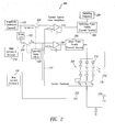
- FIG 2 is a schematic diagram of an apparatus 200 that provides the "hybrid" power supply capability as described above with reference to the graphical representations in Figures 1A-1B .
- the apparatus 200 includes or is coupleable to a linear power supply 202 and a switching power supply 204 (having a switching frequency that can be set or otherwise controlled by a unit 206, thereby providing output current pulses at a frequency corresponding to the switching frequency).
- the linear power supply 202 and the switching power supply 204 are current sources in an embodiment.
- Output terminals of the linear power supply 202 and the switching power supply 204 are in turn coupled to a first terminal of a load 208.
- a second terminal of the load 208 is coupled to ground.
- the load 208 includes at least one LED 210 for a backlight display device. In another embodiment, the load 208 includes at least one LED of a given color as part of a plurality of power supplies with different discrete colors for a backlight display device. In other embodiments, the load 208 can comprise other types of loads, including illumination and non-illumination loads, a laser device, a microwave device, that are not necessarily associated with a display device and which do not necessarily include LEDs.
- the apparatus 200 includes an amplitude command unit 212 having an output terminal to supply a linear command signal and a switching command signal to respectively control activation of the linear power supply 202 and the switching power supply 204.
- the output terminal of the amplitude command unit 212 is coupled to first switch 220, which is in turn coupled to a first input terminal of a switching power supply error amplifier 216 (e.g., a current control error amplifier or other control unit).
- the switching power supply error amplifier 216 in turn has an output terminal coupled to a control terminal of the switching power supply 204, thereby allowing output current of the switching power supply 204 to be increased or decreased based on the switching command signal at its control terminal.
- the switching power supply error amplifier 216 has a second input terminal coupled to receive a current feedback signal at 218 from the second terminal of the load 208.
- the output terminal of the amplitude command unit 212 is also coupled to a scale unit 222, which in one embodiment scales down the output command signal from the amplitude command unit 212 to Ix. In one embodiment, the scale unit 222 scales down lcmd to 2/3 of its value, although other scaling values can be provided.
- the scale unit 222 is coupled to a second switch 224, which is in turn coupled to a first input terminal of a linear power supply error amplifier 226 (e.g., another current control error amplifier or other control unit).
- the linear power supply error amplifier 226 in turn has an output terminal coupled to a control terminal of the linear power supply 202, thereby allowing output current of the linear power supply 202 to be increased or decreased based on the linear command signal at its control terminal.
- the linear power supply error amplifier 226 has a second input terminal coupled to receive the current feedback signal at 218 from the second terminal of the load 208.
- the apparatus 200 includes a PWM command unit 214 that generates the PWM enable signal 401 (described with respect to Figure 4 ) at its output terminal.
- the amplitude command unit 212 and the PWM command unit 214 can collectively comprise part of a PWM subsystem.
- the PWM enable signal 401 allows the PWM command unit 214 to control actuation of the second switch 224, such as to close the second switch 224 during the initial part of the ON duty cycle of the PWM enable signal 401 to supply the current to the load 208.
- the PWM command unit 214 has its output terminal coupled to a turn on delay unit 228 to generate switching PWM enable signal 402, control actuation of the first switch 220, and to initiate activation of the switching power supply 204.
- the delay provided by the turn on delay unit 228 is 100 microseconds, which is understood to be merely illustrative.
- the linear and switching amplitude command and the PWM duty cycle command for each color of LED power supply in the backlight are set by an outer control loop that operates to regulate luminance and color.
- the embodiment(s) of the apparatus 200 described above sufficiently addresses the disadvantages/problems of existing methods/circuits for driving backlit displays.
- Another embodiment provides further advantages by using a biasing feature to achieve a very fast turn ON. This biasing feature becomes useful at fast refresh rates (e.g., 160 Hz) and very low light levels (e.g., short pulses) due to the slow turn ON rate of the linear power supply when transitioning from a completely OFF state.
- an embodiment of the apparatus 200 of Figure 2 described above can include optional bias circuitry, which is also shown in Figure 2 .
- the bias circuitry of one embodiment includes a bias current command unit 230 coupled to the first input terminal of the linear power supply error amplifier 226 to provide a bias current command.
- Said bias current command can be provided to the load 208 in one embodiment as a bias current supplied by the linear power supply 202.
- a voltage clamping element (such as a zener diode 236 in one embodiment) is coupled in series with a third switch 234.
- the zener diode 236 and the third switch 234 are coupled in parallel to the load 208.
- An inverter 232 has an input terminal coupled to the output terminal of the PWM command unit 214 to receive the PWM enable signal 401 and to invert it.
- the inverter 232 has an output terminal coupled to the third switch 234 so that the inverted PWM enable 401 is used to control activation/deactivation of the third switch 234.
- the third switch 234 is opened during the ON portion of the duty cycle of the PWM enable signal 401 to disable the zener diode 236 and thus decouple the zener diode 236 from the load 208.
- the third switch 234 is closed during the OFF portion of the duty cycle of the PWM enable signal 401 to enable the zener diode 236 to clamp the forward voltage of the LED(s) 210 to just below turn ON voltage.
- the bias current command from the bias current command unit 230 is provided to the linear power supply error amplifier 226 during the OFF portion of the duty cycle of the PWM enable signal 401.
- the bias current command causes the linear power supply 202 to supply an output current and voltage insufficient to cause illumination due to the voltage clamping of zener diode 236, but allows faster response to drive current changes.
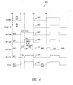
- Figure 4 provides graphical representations of the operation of a method and apparatus according to one embodiment that uses the bias circuitry, although it is understood that the operation of a method and apparatus that does not use the bias circuitry can also be ascertained from the graphical representations of Figure 4 .
- the graphical representations are merely for illustrative purposes for ease of explanation and understanding, and not necessarily drawn to scale and are also not intended to precisely depict the shape of waveforms.
- Figure 4 depicts a set 400 of waveforms/signals 401-407 that represent the relative timing between different aspects that control activation of the linear power supply 202 and the switching power supply 204 and the resulting drive current 407 (represented by the output signal 100 in Figures 1A-1B ), which is the sum of the linear output signal 405 and the switching output signal 406, supplied to the load 208.
- the PWM enable signal 401 is shown having a duty cycle with ON and OFF portions. From time t0 to t1 during the inactive portion of the duty cycle, the PWM enable signal 401 is OFF or LOW, thereby providing no enable signal to close the switches 220 and 224, which results in the linear and switching power supplies 202 and 204 providing minimal or no power to the load.
- the bias current command unit 230 provides a bias current and voltage to the load 208 during this OFF portion of the duty cycle of the PWM enable signal 401.
- the resulting scaled-down linear command signal 403 from the scale unit 222 is passed to the linear power supply error amplifier 226 at its first input terminal.
- the switching PWM enable signal 402 transitions to its full ON or HIGH level, thereby deactivating the linear power supply 202 and activating the switching power supply 204.
- the first switch 220 is closed by the switching PWM enable signal 402 from the turn on delay unit 228, and the full amplitude lcmd of the switching command signal 404 is provided by the amplitude command unit 212 to the switching power supply error amplifier 216 at its first input terminal.
- the switching power supply error amplifier 216 then senses that the feedback current at 218, received at its second input terminal from the load 208, is below the target level (e.g., below the amplitude of the switching command signal at its first input), and ramps up or otherwise activates the switching power supply 204 at time t2 to provide current (shown as the switching output signal 406) to the load 208 at the commanded level.
- the target level e.g., below the amplitude of the switching command signal at its first input
- the apparatus 200 enters the high-efficiency switching mode in which the switching power supply 204 provides switched output signal 406 to the load 208 from time t2 to t3.
- the PWM command unit 214 switches OFF the PWM enable signal 401, thereby causing the switches 220 and 224 to open, and waits for the next 160Hz period to start a new cycle at time t4.
- the bias current is at that time also provided again to the load 208, as shown as a small step increase 408 in the linear output signal 405 from the linear power supply 202.
- the process described above then repeats at the next positive (ON) portion of the duty cycle of the PWM enable signal 401.
- Figure 3 is a flowchart of an embodiment of a method 300 corresponding to Figures 1-2 and 4 to provide a hybrid power supply to the load 208.
- the apparatus 200 of one embodiment can perform the operations depicted by the method 300.
- at least some of the depicted operations can be implemented by software or other machine-readable instruction stored on a machine-readable medium and executable by a processor.
- the PWM enable signal 401 transitions from OFF to ON of the positive portion of the duty cycle.
- the linear power supply 202 is activated, as explained above, at a block 304 to supply (after an initial rise time) a current of constant linear amplitude to the load 208.
- the supplied current e.g., the linear output signal 405
- the full commanded current that can be drawn by the load 208, such as 2/3 of the commanded current.
- the bias circuitry is turned OFF at the beginning of the block 304.
- the switching power supply 204 is activated to supply current (e.g., the output signal 406) to the load 208 during the remaining ON portion of the duty cycle of the PWM enable signal 401.
- the linear power supply 202 is turned OFF at the block 306.
- the PWM enable signal 401 transitions to its OFF level, thereby turning OFF the switching power supply 204 until the next ON portion of the duty cycle of the PWM enable signal 401 and also causing the bias current and voltage to be provided to the load 208 for embodiments that use the bias circuitry.
- the method repeats as described above for blocks 302-308, at a block 310.
- the linear power supply 202 can operate for a short time, thus reducing its impact on system efficiency and component size.
- the switching power supply 204 turns on after a delay and provides discrete pulses that are small in comparison to the total PWM ON time.
- higher efficiency (such as approximately 90% efficiency, for example) resulting from the hybrid combination of power supplies provides certain advantages.
- Such advantages include, but are not limited to, reduction of load on the power supplies 202 and 204 and on the overall system, reduction in temperature of surrounding components to help improve reliability and life, and reduction in weight and size of cooling components (e.g., heat sinks and fans).
- Fast minimum pulse ON time/width (e.g., 8 microseconds max);
- Fast time step resolution (e.g., 500 nanoseconds max).
- an embodiment can provide current to the load 208 by way of the linear power supply 202 only, without using the switching power supply 204 during the active ON portion of the duty cycle of the PWM signal.
- the active ON portion of the duty cycle may be of narrow (short) length for low luminance conditions, thereby removing the need to use the switching power supply 204.
Landscapes
- Circuit Arrangement For Electric Light Sources In General (AREA)
- Dc-Dc Converters (AREA)
Applications Claiming Priority (1)
| Application Number | Priority Date | Filing Date | Title |
|---|---|---|---|
| US11/741,335 US7535183B2 (en) | 2007-04-27 | 2007-04-27 | Apparatus and method to provide a hybrid linear/switching current source, such as for high-efficiency, wide dimming range light emitting diode (LED) backlighting |
Publications (4)
| Publication Number | Publication Date |
|---|---|
| EP1986470A2 true EP1986470A2 (de) | 2008-10-29 |
| EP1986470A3 EP1986470A3 (de) | 2011-11-30 |
| EP1986470B1 EP1986470B1 (de) | 2012-12-26 |
| EP1986470B8 EP1986470B8 (de) | 2014-02-26 |
Family
ID=39684264
Family Applications (1)
| Application Number | Title | Priority Date | Filing Date |
|---|---|---|---|
| EP08251471.2A Active EP1986470B8 (de) | 2007-04-27 | 2008-04-21 | Vorrichtung und Verfahren zur Bereitstellung einer hybriden linearen Stromquelle/Schaltstromquelle, wie etwa für eine Hochleistungs-Leuchtdioden (LED)-Rückbeleuchtung mit großem Verdunkelungsbereich |
Country Status (2)
| Country | Link |
|---|---|
| US (1) | US7535183B2 (de) |
| EP (1) | EP1986470B8 (de) |
Cited By (11)
| Publication number | Priority date | Publication date | Assignee | Title |
|---|---|---|---|---|
| EP2477459A1 (de) * | 2011-01-17 | 2012-07-18 | Radiant Research Limited | Hybrides Steuerungssystem |
| EP2453296A4 (de) * | 2009-07-07 | 2012-12-19 | Sharp Kk | Flüssigkristallanzeigevorrichtung |
| EP2571334A1 (de) * | 2011-09-14 | 2013-03-20 | Alpine Electronics, Inc. | LED-Beleuchtungszeit-Steuervorrichtung |
| US8436749B2 (en) | 2010-11-03 | 2013-05-07 | Hamilton Sundstrand Corporation | Failsafe LED control system |
| EP2660805A1 (de) * | 2012-05-01 | 2013-11-06 | Hamilton Sundstrand Corporation | Ausfallsicheres LED-Steuerungssystem |
| US8816604B2 (en) | 2012-08-03 | 2014-08-26 | Ge Lighting Solutions, Llc. | Dimming control method and apparatus for LED light source |
| US8933642B2 (en) | 2011-05-13 | 2015-01-13 | General Electric Company | Dimmable LED lamp |
| WO2015128388A1 (en) * | 2014-02-26 | 2015-09-03 | Koninklijke Philips N.V. | Driver arrangement |
| DE102017107419A1 (de) | 2017-04-06 | 2018-10-11 | Vossloh-Schwabe Deutschland Gmbh | Betriebsschaltkreis und Verfahren zum Betreiben einer Leuchtmittelanordnung |
| EP2854485B1 (de) * | 2013-08-30 | 2019-06-12 | Helvar Oy Ab | PWM-Dimmen |
| CN112996186A (zh) * | 2019-12-18 | 2021-06-18 | 安徽展晖电子科技有限公司 | 脉冲控制的电路单元、驱动电路、集成电路和照明装置 |
Families Citing this family (31)
| Publication number | Priority date | Publication date | Assignee | Title |
|---|---|---|---|---|
| TWI454177B (zh) * | 2008-03-14 | 2014-09-21 | Himax Analogic Inc | 發光二極體驅動電路及用以控制功率開關之電路 |
| TWI379618B (en) * | 2008-06-30 | 2012-12-11 | Green Solution Tech Co Ltd | Led driving circuit and mos module thereof |
| US20100244711A1 (en) * | 2009-03-30 | 2010-09-30 | Richard Landry Gray | Self-Calibrating White Light Emitting Diode Module |
| CN101586751B (zh) * | 2009-04-10 | 2012-02-01 | 深圳华映显示科技有限公司 | 一种光源系统 |
| CN102014539B (zh) * | 2009-09-08 | 2013-08-21 | 群康科技(深圳)有限公司 | 背光控制电路 |
| US20110115407A1 (en) * | 2009-11-13 | 2011-05-19 | Polar Semiconductor, Inc. | Simplified control of color temperature for general purpose lighting |
| WO2011130571A1 (en) * | 2010-04-14 | 2011-10-20 | Aerovironment, Inc. | Pilot signal generation circuit |
| TWM391247U (en) * | 2010-06-14 | 2010-10-21 | Unity Opto Technology Co Ltd | Improved protection structure for LED |
| US8587212B2 (en) | 2010-08-10 | 2013-11-19 | Industrial Technology Research Institute | Lighting system, dimming control apparatus and dimming control method |
| US8872810B2 (en) | 2010-10-12 | 2014-10-28 | National Semiconductor Corporation | Combined digital modulation and current dimming control for light emitting diodes |
| US9107257B2 (en) | 2011-02-24 | 2015-08-11 | Osram Sylvania Inc. | Adaptive frequency control to change a light output level |
| JP5838346B2 (ja) * | 2011-10-24 | 2016-01-06 | パナソニックIpマネジメント株式会社 | 点灯装置および、これを用いた照明器具 |
| US9155139B2 (en) | 2012-03-09 | 2015-10-06 | Rockwell Automation Technologies, Inc. | LED driver circuits and methods |
| WO2014194081A1 (en) | 2013-05-29 | 2014-12-04 | Lutron Electronics Co., Inc. | Load control device for a light-emitting diode light source |
| KR102126534B1 (ko) * | 2013-10-31 | 2020-06-25 | 엘지디스플레이 주식회사 | 광원 구동장치 및 이를 이용한 액정표시장치 |
| US9247608B2 (en) | 2013-11-08 | 2016-01-26 | Lutron Electronics Co., Inc. | Load control device for a light-emitting diode light source |
| US9554211B2 (en) | 2014-01-03 | 2017-01-24 | Summit Semiconductor Llc | Wireless speaker unit |
| TWI501064B (zh) * | 2014-01-21 | 2015-09-21 | Celestica Technology Consultancy Shanghai Co Ltd | 混成供電架構 |
| US9456481B2 (en) * | 2014-02-25 | 2016-09-27 | Earl W. McCune, Jr. | High-efficiency, wide dynamic range dimming for solid-state lighting |
| US9565731B2 (en) | 2015-05-01 | 2017-02-07 | Lutron Electronics Co., Inc. | Load control device for a light-emitting diode light source |
| CN104837247A (zh) * | 2015-05-07 | 2015-08-12 | 成都东旭节能科技有限公司 | 四合一led电源线性调光控制电路 |
| WO2016188716A1 (en) | 2015-05-28 | 2016-12-01 | Philips Lighting Holding B.V. | Efficient lighting circuit for led assemblies. |
| WO2016205761A1 (en) | 2015-06-19 | 2016-12-22 | Lutron Electronics Co., Inc. | Load control device for a light-emitting diode light source |
| CN106028511B (zh) * | 2016-05-30 | 2017-12-29 | 上海典芯半导体有限公司 | 一种led无级调光系统 |
| EP4072247B1 (de) | 2016-09-16 | 2024-03-27 | Lutron Technology Company LLC | Laststeuerungsverfahren für eine leuchtdiodenlichtquelle mit verschiedenen betriebsarten |
| US9930743B1 (en) * | 2016-11-17 | 2018-03-27 | Infineon Technologies Austria Ag | Tunable LED |
| WO2018158640A1 (en) * | 2017-03-02 | 2018-09-07 | Awesense Wireless Inc. | Selectable power scavenging systems and methods |
| US10237936B2 (en) | 2017-08-16 | 2019-03-19 | Apple Inc. | Split driver backlight systems and methods |
| WO2019218568A1 (zh) * | 2018-05-16 | 2019-11-21 | 青岛海信电器股份有限公司 | 背光驱动电路、背光驱动方法及显示装置 |
| CN108882442B (zh) * | 2018-05-18 | 2020-04-21 | 京东方科技集团股份有限公司 | 背光源、背光源的控制方法和显示装置 |
| CN116961405A (zh) * | 2022-04-13 | 2023-10-27 | 华为技术有限公司 | 电源控制器、电源系统和控制方法 |
Family Cites Families (19)
| Publication number | Priority date | Publication date | Assignee | Title |
|---|---|---|---|---|
| WO1991000621A1 (fr) * | 1989-06-24 | 1991-01-10 | Mitsubishi Rayon Co., Ltd. | Circuit de commande de diode electroluminescente |
| US5034676A (en) * | 1990-01-12 | 1991-07-23 | Kinzalow Richard L | Direct current power supply circuit having automatic linear and switching modes |
| EP0472318A3 (en) | 1990-08-06 | 1994-08-10 | At & T Corp | Led pulse shaping circuit |
| US5903138A (en) * | 1995-03-30 | 1999-05-11 | Micro Linear Corporation | Two-stage switching regulator having low power modes responsive to load power consumption |
| US5812012A (en) * | 1996-12-09 | 1998-09-22 | Lucent Technologies Inc. | High efficiency resonant network drive for an infrared LED |
| US6095661A (en) * | 1998-03-19 | 2000-08-01 | Ppt Vision, Inc. | Method and apparatus for an L.E.D. flashlight |
| US6229289B1 (en) * | 2000-02-25 | 2001-05-08 | Cadence Design Systems, Inc. | Power converter mode transitioning method and apparatus |
| US6734639B2 (en) * | 2001-08-15 | 2004-05-11 | Koninklijke Philips Electronics N.V. | Sample and hold method to achieve square-wave PWM current source for light emitting diode arrays |
| JP3972856B2 (ja) * | 2003-04-16 | 2007-09-05 | 富士電機ホールディングス株式会社 | 電源システム |
| KR100767763B1 (ko) * | 2003-09-16 | 2007-10-17 | 노키아 코포레이션 | 폴라 송신기내에 사용되는 하이브리드 스위치드 모드/선형 전력 증폭기 전력 공급원을 구비한 무선 주파수 송신기 |
| JP3600915B1 (ja) * | 2003-10-09 | 2004-12-15 | ローム株式会社 | スイッチング電源装置及び表示装置付き電子機器 |
| US7084612B2 (en) * | 2004-04-30 | 2006-08-01 | Micrel, Inc. | High efficiency linear regulator |
| JP4429868B2 (ja) * | 2004-10-14 | 2010-03-10 | シャープ株式会社 | スイッチング電源回路及びそれを用いた電子機器 |
| CA2609877C (en) * | 2005-01-25 | 2015-05-26 | Tir Technology Lp | Method and apparatus for illumination and communication |
| EP1689212B1 (de) | 2005-02-02 | 2008-01-23 | Patent-Treuhand-Gesellschaft für elektrische Glühlampen mbH | Verfahren und Anordnung zum Dimmen von Lichtquellen |
| KR100628719B1 (ko) * | 2005-02-15 | 2006-09-28 | 삼성전자주식회사 | Led구동장치 |
| US7378805B2 (en) * | 2005-03-22 | 2008-05-27 | Fairchild Semiconductor Corporation | Single-stage digital power converter for driving LEDs |
| KR100587022B1 (ko) * | 2005-05-18 | 2006-06-08 | 삼성전기주식회사 | 디밍 회로를 갖는 led 구동회로 |
| US7498751B2 (en) * | 2006-06-15 | 2009-03-03 | Himax Technologies Limited | High efficiency and low cost cold cathode fluorescent lamp driving apparatus for LCD backlight |
-
2007
- 2007-04-27 US US11/741,335 patent/US7535183B2/en active Active
-
2008
- 2008-04-21 EP EP08251471.2A patent/EP1986470B8/de active Active
Non-Patent Citations (1)
| Title |
|---|
| None |
Cited By (15)
| Publication number | Priority date | Publication date | Assignee | Title |
|---|---|---|---|---|
| US8797253B2 (en) | 2009-07-07 | 2014-08-05 | Sharp Kabushiki Kaisha | Liquid crystal display device |
| EP2453296A4 (de) * | 2009-07-07 | 2012-12-19 | Sharp Kk | Flüssigkristallanzeigevorrichtung |
| US8436749B2 (en) | 2010-11-03 | 2013-05-07 | Hamilton Sundstrand Corporation | Failsafe LED control system |
| EP2477459A1 (de) * | 2011-01-17 | 2012-07-18 | Radiant Research Limited | Hybrides Steuerungssystem |
| US8659237B2 (en) | 2011-01-17 | 2014-02-25 | Radiant Research Limited | Hybrid power control system |
| AU2012200252B2 (en) * | 2011-01-17 | 2015-10-01 | Radiant Research Limited | Hybrid power control system |
| US8933642B2 (en) | 2011-05-13 | 2015-01-13 | General Electric Company | Dimmable LED lamp |
| EP2571334A1 (de) * | 2011-09-14 | 2013-03-20 | Alpine Electronics, Inc. | LED-Beleuchtungszeit-Steuervorrichtung |
| EP2660805A1 (de) * | 2012-05-01 | 2013-11-06 | Hamilton Sundstrand Corporation | Ausfallsicheres LED-Steuerungssystem |
| US8816604B2 (en) | 2012-08-03 | 2014-08-26 | Ge Lighting Solutions, Llc. | Dimming control method and apparatus for LED light source |
| EP2854485B1 (de) * | 2013-08-30 | 2019-06-12 | Helvar Oy Ab | PWM-Dimmen |
| WO2015128388A1 (en) * | 2014-02-26 | 2015-09-03 | Koninklijke Philips N.V. | Driver arrangement |
| US9986604B2 (en) | 2014-02-26 | 2018-05-29 | Philips Lighting Holding B.V. | Driver arrangement |
| DE102017107419A1 (de) | 2017-04-06 | 2018-10-11 | Vossloh-Schwabe Deutschland Gmbh | Betriebsschaltkreis und Verfahren zum Betreiben einer Leuchtmittelanordnung |
| CN112996186A (zh) * | 2019-12-18 | 2021-06-18 | 安徽展晖电子科技有限公司 | 脉冲控制的电路单元、驱动电路、集成电路和照明装置 |
Also Published As
| Publication number | Publication date |
|---|---|
| EP1986470B8 (de) | 2014-02-26 |
| US7535183B2 (en) | 2009-05-19 |
| EP1986470B1 (de) | 2012-12-26 |
| EP1986470A3 (de) | 2011-11-30 |
| US20080265793A1 (en) | 2008-10-30 |
Similar Documents
| Publication | Publication Date | Title |
|---|---|---|
| EP1986470B1 (de) | Vorrichtung und Verfahren zur Bereitstellung einer hybriden linearen Stromquelle/Schaltstromquelle, wie etwa für eine Hochleistungs-Leuchtdioden (LED)-Rückbeleuchtung mit großem Verdunkelungsbereich | |
| KR100898209B1 (ko) | 발광 다이오드 구동 회로 | |
| KR101370363B1 (ko) | 스위치형 광소자 어레이 및 동작 방법 | |
| JP4943892B2 (ja) | 調光装置とそれを用いた照明器具 | |
| JP4772651B2 (ja) | 発光ダイオード駆動装置及びこれを用いた液晶表示装置 | |
| KR101974090B1 (ko) | 백 라이트 구동 장치 및 액정 표시 장치 | |
| JP2006339298A (ja) | 発光素子駆動装置 | |
| KR101798437B1 (ko) | 발광 다이오드 구동회로 및 발광 다이오드 구동방법 | |
| EP3207770A1 (de) | Kombinierte hybride und lokale dimmersteuerung von leuchtdioden | |
| JP2008091311A (ja) | Led駆動装置 | |
| KR20170010212A (ko) | 백라이트 유닛 및 백라이트 유닛을 포함하는 표시 장치 | |
| JP2015088709A (ja) | Led駆動回路,led駆動方法、および液晶表示装置 | |
| KR100765268B1 (ko) | 디스플레이장치 및 그 제어방법 | |
| JP4642406B2 (ja) | 定電流駆動回路 | |
| US12592203B2 (en) | Display device, backlight control circuit and backlight control method | |
| EP2571334B1 (de) | LED-Beleuchtungszeit-Steuervorrichtung | |
| JP6460216B1 (ja) | 高光度航空障害灯の閃光駆動装置 | |
| TW201301954A (zh) | 驅動電路 | |
| JP2002056996A (ja) | 液晶バックライト調光方式 | |
| JP2007013141A (ja) | ディスプレイ装置 | |
| JP5653252B2 (ja) | 発光制御装置、表示装置、及び発光制御方法 | |
| CN114429756B (zh) | 背光扫描方法,背光驱动器以及显示设备 | |
| JP2017129813A (ja) | Ledドライバ及び表示装置 | |
| JP2018101805A (ja) | Led駆動回路,led駆動方法、および液晶表示装置 | |
| CN121195599A (zh) | 驱动电路及其方法 |
Legal Events
| Date | Code | Title | Description |
|---|---|---|---|
| PUAI | Public reference made under article 153(3) epc to a published international application that has entered the european phase |
Free format text: ORIGINAL CODE: 0009012 |
|
| AK | Designated contracting states |
Kind code of ref document: A2 Designated state(s): AT BE BG CH CY CZ DE DK EE ES FI FR GB GR HR HU IE IS IT LI LT LU LV MC MT NL NO PL PT RO SE SI SK TR |
|
| AX | Request for extension of the european patent |
Extension state: AL BA MK RS |
|
| PUAL | Search report despatched |
Free format text: ORIGINAL CODE: 0009013 |
|
| AK | Designated contracting states |
Kind code of ref document: A3 Designated state(s): AT BE BG CH CY CZ DE DK EE ES FI FR GB GR HR HU IE IS IT LI LT LU LV MC MT NL NO PL PT RO SE SI SK TR |
|
| AX | Request for extension of the european patent |
Extension state: AL BA MK RS |
|
| RIC1 | Information provided on ipc code assigned before grant |
Ipc: H05B 33/08 20060101AFI20111027BHEP Ipc: H02M 3/158 20060101ALI20111027BHEP |
|
| GRAP | Despatch of communication of intention to grant a patent |
Free format text: ORIGINAL CODE: EPIDOSNIGR1 |
|
| 17P | Request for examination filed |
Effective date: 20120529 |
|
| RIC1 | Information provided on ipc code assigned before grant |
Ipc: H05B 33/08 20060101AFI20120615BHEP Ipc: H02M 3/158 20060101ALI20120615BHEP |
|
| AKX | Designation fees paid |
Designated state(s): AT BE BG CH CY CZ DE DK EE ES FI FR GB GR HR HU IE IS IT LI LT LU LV MC MT NL NO PL PT RO SE SI SK TR |
|
| GRAS | Grant fee paid |
Free format text: ORIGINAL CODE: EPIDOSNIGR3 |
|
| GRAA | (expected) grant |
Free format text: ORIGINAL CODE: 0009210 |
|
| AK | Designated contracting states |
Kind code of ref document: B1 Designated state(s): AT BE BG CH CY CZ DE DK EE ES FI FR GB GR HR HU IE IS IT LI LT LU LV MC MT NL NO PL PT RO SE SI SK TR |
|
| REG | Reference to a national code |
Ref country code: GB Ref legal event code: FG4D |
|
| REG | Reference to a national code |
Ref country code: CH Ref legal event code: EP |
|
| REG | Reference to a national code |
Ref country code: AT Ref legal event code: REF Ref document number: 591037 Country of ref document: AT Kind code of ref document: T Effective date: 20130115 |
|
| REG | Reference to a national code |
Ref country code: DE Ref legal event code: R096 Ref document number: 602008021115 Country of ref document: DE Effective date: 20130228 |
|
| PG25 | Lapsed in a contracting state [announced via postgrant information from national office to epo] |
Ref country code: NO Free format text: LAPSE BECAUSE OF FAILURE TO SUBMIT A TRANSLATION OF THE DESCRIPTION OR TO PAY THE FEE WITHIN THE PRESCRIBED TIME-LIMIT Effective date: 20130326 Ref country code: HR Free format text: LAPSE BECAUSE OF FAILURE TO SUBMIT A TRANSLATION OF THE DESCRIPTION OR TO PAY THE FEE WITHIN THE PRESCRIBED TIME-LIMIT Effective date: 20121226 Ref country code: FI Free format text: LAPSE BECAUSE OF FAILURE TO SUBMIT A TRANSLATION OF THE DESCRIPTION OR TO PAY THE FEE WITHIN THE PRESCRIBED TIME-LIMIT Effective date: 20121226 Ref country code: SE Free format text: LAPSE BECAUSE OF FAILURE TO SUBMIT A TRANSLATION OF THE DESCRIPTION OR TO PAY THE FEE WITHIN THE PRESCRIBED TIME-LIMIT Effective date: 20121226 Ref country code: LT Free format text: LAPSE BECAUSE OF FAILURE TO SUBMIT A TRANSLATION OF THE DESCRIPTION OR TO PAY THE FEE WITHIN THE PRESCRIBED TIME-LIMIT Effective date: 20121226 |
|
| REG | Reference to a national code |
Ref country code: AT Ref legal event code: MK05 Ref document number: 591037 Country of ref document: AT Kind code of ref document: T Effective date: 20121226 |
|
| REG | Reference to a national code |
Ref country code: LT Ref legal event code: MG4D |
|
| REG | Reference to a national code |
Ref country code: NL Ref legal event code: VDEP Effective date: 20121226 |
|
| PG25 | Lapsed in a contracting state [announced via postgrant information from national office to epo] |
Ref country code: GR Free format text: LAPSE BECAUSE OF FAILURE TO SUBMIT A TRANSLATION OF THE DESCRIPTION OR TO PAY THE FEE WITHIN THE PRESCRIBED TIME-LIMIT Effective date: 20130327 Ref country code: LV Free format text: LAPSE BECAUSE OF FAILURE TO SUBMIT A TRANSLATION OF THE DESCRIPTION OR TO PAY THE FEE WITHIN THE PRESCRIBED TIME-LIMIT Effective date: 20121226 Ref country code: SI Free format text: LAPSE BECAUSE OF FAILURE TO SUBMIT A TRANSLATION OF THE DESCRIPTION OR TO PAY THE FEE WITHIN THE PRESCRIBED TIME-LIMIT Effective date: 20121226 |
|
| PG25 | Lapsed in a contracting state [announced via postgrant information from national office to epo] |
Ref country code: AT Free format text: LAPSE BECAUSE OF FAILURE TO SUBMIT A TRANSLATION OF THE DESCRIPTION OR TO PAY THE FEE WITHIN THE PRESCRIBED TIME-LIMIT Effective date: 20121226 Ref country code: CZ Free format text: LAPSE BECAUSE OF FAILURE TO SUBMIT A TRANSLATION OF THE DESCRIPTION OR TO PAY THE FEE WITHIN THE PRESCRIBED TIME-LIMIT Effective date: 20121226 Ref country code: EE Free format text: LAPSE BECAUSE OF FAILURE TO SUBMIT A TRANSLATION OF THE DESCRIPTION OR TO PAY THE FEE WITHIN THE PRESCRIBED TIME-LIMIT Effective date: 20121226 Ref country code: CY Free format text: LAPSE BECAUSE OF FAILURE TO SUBMIT A TRANSLATION OF THE DESCRIPTION OR TO PAY THE FEE WITHIN THE PRESCRIBED TIME-LIMIT Effective date: 20121226 Ref country code: SK Free format text: LAPSE BECAUSE OF FAILURE TO SUBMIT A TRANSLATION OF THE DESCRIPTION OR TO PAY THE FEE WITHIN THE PRESCRIBED TIME-LIMIT Effective date: 20121226 Ref country code: IS Free format text: LAPSE BECAUSE OF FAILURE TO SUBMIT A TRANSLATION OF THE DESCRIPTION OR TO PAY THE FEE WITHIN THE PRESCRIBED TIME-LIMIT Effective date: 20130426 Ref country code: BG Free format text: LAPSE BECAUSE OF FAILURE TO SUBMIT A TRANSLATION OF THE DESCRIPTION OR TO PAY THE FEE WITHIN THE PRESCRIBED TIME-LIMIT Effective date: 20130326 Ref country code: ES Free format text: LAPSE BECAUSE OF FAILURE TO SUBMIT A TRANSLATION OF THE DESCRIPTION OR TO PAY THE FEE WITHIN THE PRESCRIBED TIME-LIMIT Effective date: 20130406 |
|
| PG25 | Lapsed in a contracting state [announced via postgrant information from national office to epo] |
Ref country code: PT Free format text: LAPSE BECAUSE OF FAILURE TO SUBMIT A TRANSLATION OF THE DESCRIPTION OR TO PAY THE FEE WITHIN THE PRESCRIBED TIME-LIMIT Effective date: 20130426 Ref country code: PL Free format text: LAPSE BECAUSE OF FAILURE TO SUBMIT A TRANSLATION OF THE DESCRIPTION OR TO PAY THE FEE WITHIN THE PRESCRIBED TIME-LIMIT Effective date: 20121226 Ref country code: NL Free format text: LAPSE BECAUSE OF FAILURE TO SUBMIT A TRANSLATION OF THE DESCRIPTION OR TO PAY THE FEE WITHIN THE PRESCRIBED TIME-LIMIT Effective date: 20121226 Ref country code: RO Free format text: LAPSE BECAUSE OF FAILURE TO SUBMIT A TRANSLATION OF THE DESCRIPTION OR TO PAY THE FEE WITHIN THE PRESCRIBED TIME-LIMIT Effective date: 20121226 |
|
| PG25 | Lapsed in a contracting state [announced via postgrant information from national office to epo] |
Ref country code: DK Free format text: LAPSE BECAUSE OF FAILURE TO SUBMIT A TRANSLATION OF THE DESCRIPTION OR TO PAY THE FEE WITHIN THE PRESCRIBED TIME-LIMIT Effective date: 20121226 |
|
| PLBE | No opposition filed within time limit |
Free format text: ORIGINAL CODE: 0009261 |
|
| STAA | Information on the status of an ep patent application or granted ep patent |
Free format text: STATUS: NO OPPOSITION FILED WITHIN TIME LIMIT |
|
| PG25 | Lapsed in a contracting state [announced via postgrant information from national office to epo] |
Ref country code: MC Free format text: LAPSE BECAUSE OF FAILURE TO SUBMIT A TRANSLATION OF THE DESCRIPTION OR TO PAY THE FEE WITHIN THE PRESCRIBED TIME-LIMIT Effective date: 20121226 |
|
| REG | Reference to a national code |
Ref country code: CH Ref legal event code: PL |
|
| 26N | No opposition filed |
Effective date: 20130927 |
|
| GBPC | Gb: european patent ceased through non-payment of renewal fee |
Effective date: 20130421 |
|
| PG25 | Lapsed in a contracting state [announced via postgrant information from national office to epo] |
Ref country code: IT Free format text: LAPSE BECAUSE OF FAILURE TO SUBMIT A TRANSLATION OF THE DESCRIPTION OR TO PAY THE FEE WITHIN THE PRESCRIBED TIME-LIMIT Effective date: 20121226 |
|
| REG | Reference to a national code |
Ref country code: DE Ref legal event code: R097 Ref document number: 602008021115 Country of ref document: DE Effective date: 20130927 |
|
| REG | Reference to a national code |
Ref country code: IE Ref legal event code: MM4A |
|
| PG25 | Lapsed in a contracting state [announced via postgrant information from national office to epo] |
Ref country code: CH Free format text: LAPSE BECAUSE OF NON-PAYMENT OF DUE FEES Effective date: 20130430 Ref country code: LI Free format text: LAPSE BECAUSE OF NON-PAYMENT OF DUE FEES Effective date: 20130430 Ref country code: GB Free format text: LAPSE BECAUSE OF NON-PAYMENT OF DUE FEES Effective date: 20130421 Ref country code: DE Free format text: LAPSE BECAUSE OF NON-PAYMENT OF DUE FEES Effective date: 20131101 |
|
| REG | Reference to a national code |
Ref country code: DE Ref legal event code: R119 Ref document number: 602008021115 Country of ref document: DE Effective date: 20131101 |
|
| PG25 | Lapsed in a contracting state [announced via postgrant information from national office to epo] |
Ref country code: IE Free format text: LAPSE BECAUSE OF NON-PAYMENT OF DUE FEES Effective date: 20130421 |
|
| PG25 | Lapsed in a contracting state [announced via postgrant information from national office to epo] |
Ref country code: MT Free format text: LAPSE BECAUSE OF FAILURE TO SUBMIT A TRANSLATION OF THE DESCRIPTION OR TO PAY THE FEE WITHIN THE PRESCRIBED TIME-LIMIT Effective date: 20121226 |
|
| REG | Reference to a national code |
Ref country code: FR Ref legal event code: PLFP Year of fee payment: 8 |
|
| PG25 | Lapsed in a contracting state [announced via postgrant information from national office to epo] |
Ref country code: TR Free format text: LAPSE BECAUSE OF FAILURE TO SUBMIT A TRANSLATION OF THE DESCRIPTION OR TO PAY THE FEE WITHIN THE PRESCRIBED TIME-LIMIT Effective date: 20121226 |
|
| PG25 | Lapsed in a contracting state [announced via postgrant information from national office to epo] |
Ref country code: LU Free format text: LAPSE BECAUSE OF NON-PAYMENT OF DUE FEES Effective date: 20130421 Ref country code: HU Free format text: LAPSE BECAUSE OF FAILURE TO SUBMIT A TRANSLATION OF THE DESCRIPTION OR TO PAY THE FEE WITHIN THE PRESCRIBED TIME-LIMIT; INVALID AB INITIO Effective date: 20080421 |
|
| REG | Reference to a national code |
Ref country code: FR Ref legal event code: PLFP Year of fee payment: 9 |
|
| REG | Reference to a national code |
Ref country code: FR Ref legal event code: PLFP Year of fee payment: 10 |
|
| REG | Reference to a national code |
Ref country code: FR Ref legal event code: PLFP Year of fee payment: 11 |
|
| PGFP | Annual fee paid to national office [announced via postgrant information from national office to epo] |
Ref country code: FR Payment date: 20251010 Year of fee payment: 18 |
|
| PGFP | Annual fee paid to national office [announced via postgrant information from national office to epo] |
Ref country code: BE Payment date: 20251028 Year of fee payment: 18 |