EP1987343B1 - Dispositif d'essai de cisaillement - Google Patents
Dispositif d'essai de cisaillement Download PDFInfo
- Publication number
- EP1987343B1 EP1987343B1 EP07705212.4A EP07705212A EP1987343B1 EP 1987343 B1 EP1987343 B1 EP 1987343B1 EP 07705212 A EP07705212 A EP 07705212A EP 1987343 B1 EP1987343 B1 EP 1987343B1
- Authority
- EP
- European Patent Office
- Prior art keywords
- shear
- tool
- deposit
- piezo
- force
- Prior art date
- Legal status (The legal status is an assumption and is not a legal conclusion. Google has not performed a legal analysis and makes no representation as to the accuracy of the status listed.)
- Ceased
Links
Images


Classifications
-
- G—PHYSICS
- G01—MEASURING; TESTING
- G01N—INVESTIGATING OR ANALYSING MATERIALS BY DETERMINING THEIR CHEMICAL OR PHYSICAL PROPERTIES
- G01N3/00—Investigating strength properties of solid materials by application of mechanical stress
- G01N3/24—Investigating strength properties of solid materials by application of mechanical stress by applying steady shearing forces
-
- G—PHYSICS
- G01—MEASURING; TESTING
- G01N—INVESTIGATING OR ANALYSING MATERIALS BY DETERMINING THEIR CHEMICAL OR PHYSICAL PROPERTIES
- G01N19/00—Investigating materials by mechanical methods
- G01N19/04—Measuring adhesive force between materials, e.g. of sealing tape, of coating
-
- G—PHYSICS
- G01—MEASURING; TESTING
- G01N—INVESTIGATING OR ANALYSING MATERIALS BY DETERMINING THEIR CHEMICAL OR PHYSICAL PROPERTIES
- G01N2203/00—Investigating strength properties of solid materials by application of mechanical stress
- G01N2203/0014—Type of force applied
- G01N2203/0025—Shearing
-
- G—PHYSICS
- G01—MEASURING; TESTING
- G01N—INVESTIGATING OR ANALYSING MATERIALS BY DETERMINING THEIR CHEMICAL OR PHYSICAL PROPERTIES
- G01N2203/00—Investigating strength properties of solid materials by application of mechanical stress
- G01N2203/0058—Kind of property studied
- G01N2203/0091—Peeling or tearing
-
- G—PHYSICS
- G01—MEASURING; TESTING
- G01N—INVESTIGATING OR ANALYSING MATERIALS BY DETERMINING THEIR CHEMICAL OR PHYSICAL PROPERTIES
- G01N2203/00—Investigating strength properties of solid materials by application of mechanical stress
- G01N2203/02—Details not specific for a particular testing method
- G01N2203/06—Indicating or recording means; Sensing means
- G01N2203/0617—Electrical or magnetic indicating, recording or sensing means
- G01N2203/0623—Electrical or magnetic indicating, recording or sensing means using piezoelectric gauges
Definitions
- This invention concerns apparatus and methods for testing the shear strength of a bond in a semi-conductor device, and more particularly the strength of a bond between a substrate and a means of electrical connection thereto, typically a part-spherical deposit.
- Such deposits can be of solder, gold or other materials and are sometimes referred to as solder bumps or ball grid arrays.
- Semiconductor devices are very small, typically from 0.2 mm square to 25 mm square. These devices have sites for the bonding of electrical conductors thereto. Sites typically comprise part spherical electrically conductive deposits of for example gold or solder, collectively known as balls, which in use have the appearance of a squashed sphere or low circular dome, and a diameter in the range 50-1000 ⁇ m. These deposits form part of the electrical path between, for example, a printed circuit board and a chip, and may directly connect components, or may be joined to a conductor which is itself connected to another component. Many such balls may be provided as a regular grid-like array on a substrate.
- Discrete balls are typically applied to a substrate and reflowed during subsequent connection to another component.
- a known shear test apparatus comprises a machine having a support surface and a test head movable in a controlled manner relative to the support surface.
- the test head carries a cartridge specific to the test to be performed and having one of several interchangeable tools thereon.
- the tool will be sized and/or shaped to suit the ball deposit to be tested.
- the substrate to be tested is attached to the support surface, and the tool is mounted into the cartridge and driven against the ball deposit to perform the required test, which may be for example a shear test or a reciprocating fatigue test.
- the tool moves against a stationary deposit.
- a typical tool is very small, and accordingly the cartridge has a flexible element on which is mounted one or more force gauges (such as strain gauges).
- force gauges such as strain gauges.
- WO2006/016136 discloses a shear test apparatus for gold and solder balls of a semi-conductor substrate comprising a support element on which is provided a piezo electric crystal in the direct shear load path.
- a test apparatus for applying shear loads to a ball deposit of electrically conductive material on a substrate, the apparatus comprising a support element, and a piezo-electric crystal on the support element, the support element being adapted to apply a shear load to a ball deposit, and said crystal being arranged to be placed under stress, thus causing an electrical signal to emanate therefrom.
- the electrical signal is processed to provide a measure of the shear force experienced by the support element, which in the preferred embodiment is a shear tool.
- Electrical connection to the crystal may be by means of conventional wiring, for example a pair of flexible electrical conductors of suitable cross-sectional area.
- the electrical pathways may be provided via the material of the support element on which the piezo-electric crystal is mounted. Insulation to separate the electrical feed and return may be provided in any conventional manner, for example by external insulation of flexible wires, or by a dielectric material separating components of a support element, or by a combination of these.
- the support element provides electrical feed and return pathways whereas in another embodiment insulated flexible wires provide the feed and return electrical pathways.
- the piezo-electric crystal is applied to the back face of the shear tool, or support element, the front face being adapted to apply said shear load.
- the front face which is adapted to contact the ball deposit is necessarily placed in tension as its shears the ball deposit of the substrate.
- the opposite, back, face provides a convenient mounting for a piezo-electric crystal. While the front face it is placed in tension as the ball deposit a sheared, at the same time, the back face is necessarily placed in compression and the piezo element mounted on to the back face is stressed by the compressive forces acting along the back face.
- the mounting face of the crystal is planar and closely adjacent the portion of the support element which is adapted to contact the ball deposit, in use.
- the piezo-electric crystal can be of any suitable shape or thickness. Generally speaking one face thereof is preferably planar, most preferably flat, to permit mounting to the support element. A crystal may be calibrated to determine the relationship between stress and electrical output, and the shape thereof may be selected to give a desirable characteristic. In the preferred embodiment the crystal is a rectangular planar member having substantially equal transverse dimensions and in edge alignment with the Z axis and it is mounted on the back side of the support element which is subjected to compressive strain when shearing a ball deposit as discussed above.
- the exemplary apparatus envisages one or more piezo-electric crystals mounted on a support element and arranged to be placed under stress in different directions with respect to the direction of application of force.
- the exemplary apparatus may include electronic resolution of inputs from several piezo-electric crystals so as to obtain information about the direction of failure force on a ball deposit.
- the support element is retained by a tool holder which in turn is mounted in a known shear test machine having capability of movement in the X, Y and Z axes.
- Such an arrangement provides a convenient means of adapting a shear test machine to different shear tests, in particular by allowing the shape of the support element to be selected according to the nature and shape of the ball deposit, and the likely shear forces to be applied.
- ball deposits of larger size and likely having better adherence can be tested with a support element of appropriate size.
- the output range of the piezo-electric crystal can be optimised to give high sensitivity in the range of shear force anticipated.
- the shape of the support element in the region of contact with the ball deposit can be selected to suit the intended test, for example from a range comprising a flat planar contact face, a one dimensional curved contact face adapted to the approximate diameter of the ball deposit, and a two-dimensional curved contact face adapted to the approximate sphericity of the ball deposit. It will be understood that ball deposits are typically somewhat irregular in shape, so that an approximation of the size and shape of contact face is required.
- the support element may for example be a substantially rectangular block having parallel front and rear faces, the front face having the contact face for the ball deposit, and the back face having the piezo-electric crystal mounted thereon.
- the support element is a spade-like tool having a flat back face to which said crystal is mounted.
- the front face of the support element may be adapted to the shape of the ball deposit to be tested, for example by having a part spherical recess adapted to engage a portion of the circumference of the ball deposit.
- the contact face of the support element may be reduced in size to correspond closely to the diameter of the ball deposit to be tested.
- the support element may comprise a main body portion to which the piezo-electric crystal is mounted, and a protruding contact portion of reduced size.
- the main body portion can be sized to accommodate a piezo-electric crystal of desired proportions regardless of the size of the contact portion.
- the contact portion may be made small enough to engage individual but closely adjacent ball deposits, without requiring a correspondingly small support element and piezo-electric crystal.
- the base of the contact portion may also be made small enough to land upon a flat portion of a substrate between closely adjacent ball deposits, so as to ensure a precise lifting distance off of the substrate prior to a shear test; as noted in the introduction such lift is necessary to avoid rubbing friction.
- variation of the proportions of the support element relative to the proportions of the contact portion permits the range of stress in the region of the piezo-electric crystal to be selected; thus a preferred size and shape of piezo-electric crystal may be adapted to a range of differently sized and shaped contact portions.
- the piezo-electric crystal may be mounted to the support element in any suitable manner which allows stress to be transmitted thereto in a consistent and repeatable manner.
- One suitable method of mounting is surface bonding by an adhesive such as epoxy resin.
- the interface between the support element and the crystal comprises a force distributing layer which is adapted to give substantially uniform planar contact.
- a force distributing layer may for example comprise an epoxy resin which is spread whilst fluid onto the respective interface surfaces, and cures after assembly of the apparatus to ensure that planar contact occurs.
- the layer need only be very thin, and sufficient only to accommodate any misalignment which may be present in the respective surfaces.
- a particular advantage of epoxy resin is that the adjacent components are also retained in one another adhesively, so that the apparatus becomes unitary.
- the adhesive layer comprises a thin cushion between the support element and the piezo-electric crystal, and has the second function of mechanically retaining the support element and piezo-electric crystal in permanent robust engagement.
- the layer of epoxy resin may also provide an electrical insulator for the crystal or, depending on the electrical pathways, may be electrically conductive. Such an arrangement is particularly advantageous in cases where one or more flexible wires is considered undesirable.
- the support element is provided with an inset contact portion for contact with the ball deposit.
- the contact face is typically set back by 30-60% of the overall width of the support element.
- the plane of the inset is preferably orthogonal to the intended direction of application of shear force, and is typically substantially orthogonal to the substrate and in the Z axis. In one embodiment the plane of the inset is parallel to and between planes defining the front and back faces of the support element.
- the exact location of the inset face is preferably determined so that vertical loads on the underside of the tool pass through a neutral plane with respect to the mounting face of the piezo-electric crystal, so that the output thereof is not affected.
- This adaptation and/or interpretation of the electrical output of the piezo-electric crystal is not required; in particular the electrical output is preferably proportional to the strain exerted thereon, and to the applied shear force. Most preferably the relationship between applied shear force and electrical output is linear.
- the location of the inset is determined by the required shape and dimensions of the support element, but can be predicted by the use of mathematical methods such as finite element analysis (FEA) and checked by empirical application of vertical (Z direction) loads.
- FEA finite element analysis
- the inset is orthogonal to the intended direction of shear, and is connected to the front face of the support element by an angled or radiused face so as to eliminate points or lines of high stress.
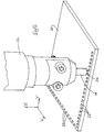
- a tool holder 11 comprises a tubular body 12 having a reduced diameter shank 13 for attachment to a test machine such as the bond test machine 100 schematically illustrated in Figure 1A .
- the shank 13 is secured in the machine by means of a collet chuck or the like such as chuck 102 of Figure 1A .
- the tubular body 12 is for example of metal, preferably a suitably stiff material such as steel.
- Pressed into the mouth of the tubular body 12 is an annular insulator 14 of any suitable dielectric material, such as a non-conductive plastic.
- Pressed into the insulator 14 is a tool holder 15 of e.g. steel, and having a split clamp 16 at the proximal end comprising a removable cap 17 secured by socket head screws 20, as illustrated.
- the split clamp 16 allows insertion and removal of a support element, or shear tool, 18 on which is mounted a piezo-electric crystal 19.
- the shear tool is of ceramic material, and comprises a flat plate of substantially constant thickness.
- the tool 18 is housed in a corresponding recess of the tool holder so that it is retained and gripped when the screws 20 are tightened.
- the shear tool 18 is mounted as a cantilevered beam, with the piezo-electric crystal 19, mounted along the central area of the length of the beam.
- This invention relates to a device for testing the shear strength of a bond in a semiconductor device and more specifically to a shear tool assembly comprising shear tool 18 and crystal 19.
- Removable mounting of the tool holder 11 in a test machine is desirable, but not essential, and in the case of removable mounting, the means of mounting is not important save that a suitably rigid and secure connection is ensured.
- a removable shear tool 18 is not essential, but may be advantageous to permit different shear tools to be fitted to a common tool holder 16. It will be understood that a shear tool 18 may be fixed in a test machine so as to be semi-permanent; in other words removable thereof is envisaged only in case of breakage or other kind of malfunction. Such an arrangement would be beneficial in the event of repeated testing of the same component, where a removable tool holder and/or shear tool may be beneficial in the case of frequent changes in test procedure and/or product.
- tool holder and shear tool could be permanently connected, for example by epoxy adhesive, in which case a removable cap 17 is not required.
- Bond testing machines capable of doing ball deposit shear tests are available in the art.
- One example is the Model 4000 Series machine available from Dage Precision Industries, Ltd. of Aylesbury, United Kingdom.
- Figure 13 schematically illustrates a bond test machine having many elements in common with Model 4000 machine.
- the shank 13 of the tool holder 11 which holds shear tool 18 is secured in a chuck 102 which is in turn mounted on a tool mover 104.
- Tool mover 104 provides movement in the X direction, for example, of the shear tool 18 to shear a ball deposits 23 off substrate 22 and movement in the Z direction to vertically position the shear tool 18 with respect to the ball deposits 23.
- Substrate 22 is mounted on table 118 which provides for movement of the substrate in the X and Y directions relative to shear tool 18.
- Tool mover 104 is secured to a housing 105 upon which is mounted a high-powered microscope 106.
- Housing 105 can also include the processor which processes the electrical signals received from the piezo-electric crystal 19 and preferably displays the results of that processing on a display screen 107 which is attached to the housing 105.
- the machine 100 also includes joystick controls 106, 108 which move the X-Y table 118 and shear tool 18. The operator looks through the high-powered microscope 106 at the area of the substrate 22 of interest and uses the joy sticks 106, 108 to position the shear tool 18 adjacent to the ball deposit 23 to be sheared off of the substrate 22.
- the tool mover 104 moves the tool 18 a desired distance in the X direction, at a desired speed, to shear the ball deposit 23 off of the substrate 22.
- the piezo-electric crystal 19 experiences forces of tension and compression in a manner later described in more detail. The forces which act upon the piezo-electric crystal 19 produce an electric signal from the crystal 19 which can be correlated to the shear force required to shear the ball deposit 23 off of the substrate.
- the electric signal produced by the piezo-electric crystal can be conveyed by insulated wires (not shown) passing through the aperture 5 within the body 12 to exit at the distal end 21 and then up into the processor (not shown) contained within housing 105.
- suitable electric tracks may be formed by photo-resist printing on the surface of a ceramic shear tool 18, and provided with push-on electrical connections at the surfaces at which the tool is secured to the tool holder 15.
- the ceramic shear tool 18 provides the dielectric material onto which the conductive tracks are provided.
- Conductive tracks may be provided in other ways, for example by bonding or otherwise fixing metallic elements to the ceramic tool 18.
- the tip 24 of the shear tool 18 is reduced in width, as illustrated best in Figure 4 to correspond closely to the actual width of the connection balls to be tested.
- the shear tool 18 typically has a width/thickness proportion in the range 3:1 to 8:1, and the tip 24 is typically 1000 ⁇ m or less. As illustrated the ratio of the width of the tip 24 to the width of the shear tool 18 may be in the range 4:1 to 10:1.
- Fig. 5 shows a test tool in use.
- the body 12 of the tool holder is mounted on a suitable test machine such as the one shown in Figure 1A having X, Y, Z traverse as depicted and as previously described is moved relative to a substrate 22 so as to be in position to apply a shear force to one of a number of ball deposits 23.
- Suitable contact sensing apparatus may be provided to ensure that drag of the shear tool 18 on the substrate 22 is avoided while the shear tool 18 is shearing the ball deposit 23 off the substrate 22.
- Two edge rows of balls 23 are illustrated, but any shape of array may be encountered, including a grid array covering the face of substrate 23.
- the test is performed by moving the shear tool 18 against the respective ball 23 in the 'X' direction, and applying a progressively increasing force until breakage occurs.
- the test may alternatively be performed by moving the shear tool 18 at speed, for example at a speed in the range 0.5 to 2.5 m/sec relative to the ball deposit 23 to dynamically shear the ball deposit 23 off of substrate 22.
- the speed of tool movement may be up to 10 m/sec dependent on the capabilities of the apparatus, but generally speaking the lowest speed commensurate with effective testing is suitable.
- the shear tool 18 is cantilevered out from the body 12 so that in use loads on the front face of the shear tool 18 experienced while the tool 18 is shearing a ball deposit 23 of the substrate 22 place that face in tension.
- the rear face is placed correspondingly in compression. Accordingly the piezo-electric crystal 19 is stressed by the compressive forces acting on the rear face and the crystal 19 generates an electrical output which can be used to determine the force required to shear the ball 23 of the substrate 22.
- Tests may be repeated for some or all of the ball deposits of a substrate, and in the case of a regular array the test may be automated.
- This embodiment describes use of a single piezo-electric crystal having an aperture compressive axis generally in the Z direction, orthogonal to the plane of movement during shear testing. If necessary or convenient, several crystals may be utilized to detect strain in several mutually different directions, and the several electrical outputs be used severally or in combination to resolve shear force in a desired direction of interest.
- the tool 18 may be calibrated by repeated shearing of a material of known size and quality, for example a wire end indexed upwardly through a close fitting hole in a substrate. According to this method, a fixture holding the test wire would be secured on the table 118. The shear tool 18 would then be positioned adjacent to the wire end in the same way in which it is positioned relative to a ball deposit. The machine would then be activated to shear off the end of the test wire. Given that the test wire is of a known material and geometry, the forces required to shear the test wire are known. Thus, the electric signal produced by the piezo-electric crystal 19 can be correlated to a known sheer force values.
- a tool holder 41 has a mounting shank 43 and a mouth 44 having opposed 'V' grooves 45 to receive a shear tool insert 46.
- the insert slides 46 into the holder 41 along the axis of the grooves 45 and into abutment with a stop plate 47.
- the insert 46 is arranged to be retained by a spring loaded ball catch (not shown), and secured by a grub screw 48 so that it becomes immovable with respect to the tool holder 41.
- a ceramic shear tool 49 having a front face 50 for contact with a ball deposit, and a back face 51 having a piezo-electric crystal 52 mounted thereon.
- shear loads applied at the front face to ball deposits 23 cause a compressive stress to be applied to the crystal 52 with a resulting electrical output.
- the tool 49 has similar overall proportions to the tool illustrated in the first embodiment.
- Suitable sliding electrical connections 53 are provided between the piezo-electric element 52 of insert 46 and the tool holder 41, so as to engage automatically by brushing as the tool holder 41 is inserted.
- the contact face 54 of the shear tool 49 is set back from the front face as illustrated.
- vertical forces are also generated.
- the vertical forces if significant, affect the output of the crystal 52 and may be sufficient to distort the measured forces. Ideally, only the horizontal force necessary to shear the ball deposit off for the substrate should be registered by the crystal 19.
- the vertical forces can be directed into a neutral plane so that measurement of bending stress and strain at the mounting face is relatively undistorted.
- the contact face 54 is set back a distance 120 which, in this embodiment, is approximately 40% of the distance 122 from the front face 50 to the back (mounting) face 51.
- the actual set back 120 selected for a particular shear tool 49 is dependent on the overall dimensions of the shear tool 49 and the size and position of the piezo crystal 52.
- the set back 120 may also be influenced by the shape of the ball deposit, and the form of the contact face 52.
- the size of set back 120 is typically in the range 30-60% and can be determined empirically from testing, by mathematical methods such as finite element analysis (FEA), and from application of vertical loads to the underside of the tool 49 whilst observing the output of the crystal 52.
- FEA finite element analysis
- the size of the bending moment is a function of the moment arm, or distance, 216 between the contact face 200 and the root of the tool 202.
- the horizontal force 210 places the front face 204 of the tool in tension and the rear face 206 in compression as previously described.
- piezo-electric crystal 220 experiences a compressive force 230 produced by the horizontal force 210, a compressive force 232 corresponding to the vertical force 212, and a force 234 placing the crystal 220 in tension corresponding to the bending moment 214.
- the tension force 234 is likely to be more significant than the compressive force 232 with the result that this tension force 234 will tend to cancel a part of the force 230, resulting in an inaccurate sheer force measurement.
- the contact face 300 of the shear tool 302 is offset rearwardly from the front face 304.
- the effect of this offset is to bring the contact face 300 closer to the center of bending 318 of the tool 302.
- the result is that the tool 302 still experiences the same horizontal force 310 which results from a ball deposit 23 pushing back against the tool 302.
- the tool 302 also experiences the same vertical force 312 caused by the ball deposit 23 pushing up on the tool 302.
- the moment arm 308 has been shortened, the bending moment 314 has been correspondingly reduced compared to the bending moment 214 in Figure 10 .
- the piezo-element 320 still experiences the same compressive force 330 corresponding to the horizontal force 310, and the same compressive force 332 corresponding to the vertical force 312, the tension force 334 resulting from the bending moment 314 is significantly reduced.
- the geometry of the tool is designed such that the tension force 334 resulting from the bending moment 314 is roughly equivalent to the compression force 332 with the result that these forces substantially cancel each other out so that the piezo-electric crystal 320 produces an electrical signal corresponding only to the compressive force 330 which results from the horizontal force 310. In this way, the crystal 320 is producing a force that more accurately reflects just the amowit of force necessary to shear the ball deposit 23 off of substrate 22.
- Fig.12 shows a three dimensional representation of a stepped-back tool 49 prior to application of a shear force to one of a row of ball deposits.
- the width of the contact face 54 is approximately the same as the diameter of the ball deposit, and may be about 100-750 ⁇ m.
- the use of a replaceable inset permits different widths of tool to be provided, and tools with different form (for example tools having a shaped recess adapted to the shape of the ball deposit).
Landscapes
- Physics & Mathematics (AREA)
- Health & Medical Sciences (AREA)
- Life Sciences & Earth Sciences (AREA)
- Chemical & Material Sciences (AREA)
- Analytical Chemistry (AREA)
- Biochemistry (AREA)
- General Health & Medical Sciences (AREA)
- General Physics & Mathematics (AREA)
- Immunology (AREA)
- Pathology (AREA)
- Investigating Strength Of Materials By Application Of Mechanical Stress (AREA)
Claims (16)
- Appareil de test destiné à appliquer des forces de cisaillement à un dépôt électriquement conducteur (23) sur un substrat (22) pour tester la résistance au cisaillement de la liaison entre eux, l'appareil comprenant un outil de cisaillement (18, 49, 202, 302), et un cristal piézoélectrique (19, 52, 220, 320) monté sur l'outil de cisaillement (18, 49, 202, 302), l'outil de cisaillement (18, 49, 202, 302) étant adapté pour appliquer une force de cisaillement sur ledit dépôt (23), et ledit cristal (19, 52, 220, 320) étant agencé pour être placé sous une contrainte causée par des forces de compression ou de tension agissant le long dudit outil de cisaillement (18, 49, 202, 302) pendant que ledit outil de cisaillement (18, 49, 202, 302) applique ladite force de cisaillement sur ledit dépôt (23), ledit cristal (19, 52, 220, 320) produisant un signal électrique en réponse à ladite contrainte, ledit signal électrique fournissant une indication de la force de cisaillement requise pour cisailler le dépôt (23) et le séparer du substrat (22), dans lequel ledit outil de cisaillement (18, 49, 202, 302) comporte une face frontale (50, 204) et une face arrière (51, 206), la face frontale (50, 204) étant adaptée pour appliquer ladite force de cisaillement sur ledit dépôt (23), caractérisé en ce que le cristal piézoélectrique (19, 52, 220, 320) est monté sur la face arrière (51, 206).
- Appareil selon la revendication 1 dans lequel l'outil de cisaillement (18, 49, 202, 302) comprend une partie de corps principale sur laquelle est monté le cristal piézoélectrique (19, 52, 220, 320), et une partie de contact saillante (24) de dimension réduite.
- Appareil selon la revendication 1 dans lequel ledit outil de cisaillement (18, 49, 202, 302) est doté d'une partie de contact destinée à faire contact avec le dépôt de bille (23), et dans lequel ladite partie de contact est décalée vers l'arrière à partir de ladite face frontale.
- Appareil selon la revendication 2 ou la revendication 3 dans lequel ladite partie de contact comprend une face de contact (54, 200, 300) en retrait à partir de ladite face frontale (50, 204) par un décalage qui est 30 à 60% de la largeur globale dudit outil de cisaillement (18, 49, 202, 302).
- Appareil selon la revendication 4 dans lequel le plan du décalage est orthogonal à la direction d'application de ladite force d'application.
- Appareil selon n'importe quelle revendication précédente dans lequel la relation entre la force de cisaillement appliquée et la sortie électrique est proportionnelle.
- Appareil selon la revendication 6 dans lequel la relation entre la force de cisaillement appliquée et la sortie électrique est linéaire.
- Appareil selon n'importe quelle revendication précédente, comportant en outre un porte-outil (11, 15, 41) auquel est fixé ledit outil de cisaillement (18, 49, 202, 302), ledit porte-outil (11, 15, 41) étant adapté pour être fixé à un dispositif de déplacement d'outil.
- Appareil selon la revendication 8 dans lequel ledit porte-outil (11, 41) définit une embouchure (44) dans laquelle est retenu ledit outil de cisaillement (49).
- Appareil selon la revendication 9 dans lequel ledit porte-outil (11, 15) comprend une pince fendue définissant ladite embouchure, et étant actionnable pour saisir ledit outil de cisaillement (18).
- Appareil selon la revendication 10 dans lequel ledit porte-outil (15) comprend un corps et un capot amovible (17) fixé à celui-ci par des vis (20), lesdits corps et capot (17) définissant ladite pince fendue et ledit capot (17) étant réglable relativement audit corps par l'actionnement desdites vis (20) afin de saisir ledit outil de cisaillement (18).
- Appareil selon la revendication 8 dans lequel lesdits porte-outil (41) et outil de cisaillement (49) comprennent des formes mâle et femelle complémentaires permettant la connexion sur un même axe linéaire perpendiculaire à la direction de cisaillement dudit outil de cisaillement (49).
- Appareil selon la revendication 12 dans lequel ledit outil de cisaillement (49) comprend des glissières saillantes opposées destinées à être reçues dans des évidements pour glissières correspondants (45) dudit porte-outil (41).
- Appareil selon la revendication 13 et comportant une butée (47) destinée à limiter l'insertion dudit outil de cisaillement (49) dans ledit porte-outil (41), et comportant en outre une pince libérable pour retenir ledit outil de cisaillement (49) dans ledit porte-outil (41).
- Appareil selon l'une quelconque des revendications 12 à 14 et comportant en outre des contacts électriques coopérants (53) adaptés pour se coupler à la connexion dudit outil de cisaillement (49) et dudit porte-outil (41).
- Appareil selon la revendication 15 dans lequel lesdits contacts électriques (53) comprennent des balais coulissants engageables automatiquement dans la direction dudit axe.
Applications Claiming Priority (3)
| Application Number | Priority Date | Filing Date | Title |
|---|---|---|---|
| GB0603243A GB0603243D0 (en) | 2006-02-17 | 2006-02-17 | Shear test device |
| GB0621462A GB0621462D0 (en) | 2006-10-27 | 2006-10-27 | Shear test device |
| PCT/GB2007/000528 WO2007093799A1 (fr) | 2006-02-17 | 2007-02-16 | Dispositif et procédé d'essai de cisaillement |
Publications (2)
| Publication Number | Publication Date |
|---|---|
| EP1987343A1 EP1987343A1 (fr) | 2008-11-05 |
| EP1987343B1 true EP1987343B1 (fr) | 2021-07-21 |
Family
ID=37983518
Family Applications (1)
| Application Number | Title | Priority Date | Filing Date |
|---|---|---|---|
| EP07705212.4A Ceased EP1987343B1 (fr) | 2006-02-17 | 2007-02-16 | Dispositif d'essai de cisaillement |
Country Status (4)
| Country | Link |
|---|---|
| US (1) | US7905152B2 (fr) |
| EP (1) | EP1987343B1 (fr) |
| JP (1) | JP5060494B2 (fr) |
| WO (1) | WO2007093799A1 (fr) |
Families Citing this family (12)
| Publication number | Priority date | Publication date | Assignee | Title |
|---|---|---|---|---|
| EP2570790B1 (fr) * | 2004-08-10 | 2015-11-04 | Dage precision Industries Ltd. | Procédé d'essai de cisaillement |
| GB0613205D0 (en) | 2006-07-03 | 2006-08-09 | Dage Prec Ind Ltd | High speed test cartridge |
| EP2363701B1 (fr) | 2010-03-05 | 2015-11-04 | Nordson Corporation | Mécanisme de serrage amélioré pour appareil de test de cisaillement |
| EP2386845B1 (fr) | 2010-05-14 | 2024-03-13 | Nordson Corporation | Procédé et système pour tester les soudures d'un ensemble semi-conducteur |
| RU2511624C1 (ru) * | 2012-11-06 | 2014-04-10 | Федеральное государственное бюджетное образовательное учреждение высшего профессионального образования Казанский национальный исследовательский технический университет им. А.Н. Туполева-КАИ" (КНИТУ-КАИ) | Способ проведения испытаний на сдвиг и устройство для его реализации |
| CN103575651A (zh) * | 2013-11-25 | 2014-02-12 | 山东省建筑科学研究院 | 砌体通缝切向粘结强度测试仪及测试方法 |
| DE102015111328A1 (de) | 2015-07-13 | 2017-01-19 | Fraunhofer-Gesellschaft zur Förderung der angewandten Forschung e.V. | Prüfvorrichtung und Verfahren zur Ermittlung einer Abreißfestigkeit |
| CN110567810B (zh) * | 2019-10-28 | 2022-07-12 | 山东大庚工程材料科技有限公司 | 一种钢塑格栅拉伸检测装置 |
| US20220270937A1 (en) * | 2021-02-23 | 2022-08-25 | Kulicke And Soffa Industries, Inc. | Methods of determining shear strength of bonded free air balls on wire bonding machines |
| CN113624938B (zh) * | 2021-07-19 | 2023-12-01 | 深圳市德瑞茵精密科技有限公司 | 半导体微焊点强度测试工具保护装置及测试设备 |
| KR102573040B1 (ko) * | 2021-08-20 | 2023-08-31 | 에이티아이 주식회사 | 시료 표면의 범프 결합 강도 측정 장치 |
| CN116973246A (zh) * | 2022-04-21 | 2023-10-31 | 先进科技新加坡有限公司 | 对互连键合件进行剪切测试的方法和装置 |
Family Cites Families (29)
| Publication number | Priority date | Publication date | Assignee | Title |
|---|---|---|---|---|
| GB1094862A (en) | 1964-03-31 | 1967-12-13 | Ether Eng Ltd | Improvements in and relating to strain gauges |
| GB1208382A (en) | 1968-03-23 | 1970-10-14 | Ferranti Ltd | Improvements relating to semiconductor strain transducers |
| US3603152A (en) | 1970-02-05 | 1971-09-07 | Columbia Research Lab Inc | Transducer for detecting pressure changes in fluid flow |
| DE2102684C3 (de) | 1971-01-21 | 1980-02-28 | Friedrich Kocks Gmbh & Co, 4000 Duesseldorf | Vorrichtung zum Durchtrennen von Walzdraht |
| US3821785A (en) | 1972-03-27 | 1974-06-28 | Signetics Corp | Semiconductor structure with bumps |
| US3805601A (en) | 1972-07-28 | 1974-04-23 | Bell & Howell Co | High sensitivity semiconductor strain gauge |
| US4280350A (en) | 1979-12-10 | 1981-07-28 | Consolidated Foods Corporation | Wire bending system |
| GB2174241A (en) | 1985-04-25 | 1986-10-29 | Transamerica Delaval Inc | Transducer devices |
| JPH0733990B2 (ja) | 1987-12-29 | 1995-04-12 | 三井造船株式会社 | 打撃検査装置 |
| US4869043A (en) | 1988-08-02 | 1989-09-26 | Fero Holdings Ltd. | Shear connector |
| SU1727039A1 (ru) | 1989-12-04 | 1992-04-15 | Московский институт радиотехники, электроники и автоматики | Устройство дл определени адгезионной прочности покрытий |
| US5178005A (en) * | 1990-07-02 | 1993-01-12 | Western Atlas International, Inc. | Sample sleeve with integral acoustic transducers |
| US5166910A (en) * | 1991-10-15 | 1992-11-24 | Atlantic Richfield Company | Method and apparatus for measuring the acoustic velocity |
| JPH05203550A (ja) * | 1992-01-24 | 1993-08-10 | Shimadzu Corp | 界面強度測定方法及びその測定装置 |
| US5479683A (en) | 1993-12-29 | 1996-01-02 | Bausch & Lomb Incorporated | Three-dimensional eyewinder apparatus |
| KR0186084B1 (ko) | 1995-09-02 | 1999-04-15 | 문정환 | 히팅장치를 구비한 웨지 공구 |
| NL1001532C1 (nl) | 1995-10-31 | 1997-05-02 | Gerold Staudinger | Inrichting voor het beproeven van verbindingen tussen een (electronisch) bouwelement en een van geleidende sporen voorziene drager. |
| US6041996A (en) | 1996-11-22 | 2000-03-28 | Matsushita Electric Industrial Co., Ltd. | Method of pressure bonding a bumped electronic part and an apparatus for pressure bonding a bumped electronic part |
| US6131795A (en) | 1997-11-10 | 2000-10-17 | Matsushita Electric Industrial Co., Ltd. | Thermal compression bonding method of electronic part with solder bump |
| US5938503A (en) * | 1997-11-25 | 1999-08-17 | Edo Western Corporation | Active centering apparatus with imbedded shear load sensor and actuator |
| GB9910362D0 (en) | 1999-05-06 | 1999-06-30 | Dage Precision Ind Ltd | Test apparatus |
| AUPQ077899A0 (en) | 1999-06-04 | 1999-06-24 | University Of Sydney, The | A device for evaluating the dynamic mechanical properties of materials |
| EP1442274A1 (fr) | 2001-10-30 | 2004-08-04 | Board of Trustees of Michigan State University | Detecteur de debit a fil ou a film chauds oscillants |
| GB0219910D0 (en) | 2002-08-28 | 2002-10-02 | Koninkl Philips Electronics Nv | Wedge-bonding of wires in electronic device manufacture |
| US7059512B2 (en) | 2002-11-06 | 2006-06-13 | Ricoh Company, Ltd. | Solder alloy material layer composition, electroconductive and adhesive composition, flux material layer composition, solder ball transferring sheet, bump and bump forming process, and semiconductor device |
| WO2004083831A1 (fr) | 2003-03-19 | 2004-09-30 | Dage Precision Industries Ltd. | Sonde blindee pour testeur de soudures |
| GB0411057D0 (en) * | 2004-05-18 | 2004-06-23 | Dage Prec Ind Ltd | Test apparatus |
| EP2570790B1 (fr) | 2004-08-10 | 2015-11-04 | Dage precision Industries Ltd. | Procédé d'essai de cisaillement |
| WO2006118545A2 (fr) | 2005-04-29 | 2006-11-09 | Agency For Science, Technology And Research | Appareil d'essai de micro-impact |
-
2007
- 2007-02-16 EP EP07705212.4A patent/EP1987343B1/fr not_active Ceased
- 2007-02-16 US US12/161,055 patent/US7905152B2/en active Active
- 2007-02-16 JP JP2008554843A patent/JP5060494B2/ja not_active Expired - Fee Related
- 2007-02-16 WO PCT/GB2007/000528 patent/WO2007093799A1/fr not_active Ceased
Non-Patent Citations (1)
| Title |
|---|
| None * |
Also Published As
| Publication number | Publication date |
|---|---|
| US7905152B2 (en) | 2011-03-15 |
| JP2009526987A (ja) | 2009-07-23 |
| WO2007093799A1 (fr) | 2007-08-23 |
| EP1987343A1 (fr) | 2008-11-05 |
| JP5060494B2 (ja) | 2012-10-31 |
| US20100116063A1 (en) | 2010-05-13 |
Similar Documents
| Publication | Publication Date | Title |
|---|---|---|
| EP1987343B1 (fr) | Dispositif d'essai de cisaillement | |
| US8312777B2 (en) | Test device | |
| EP2363701B1 (fr) | Mécanisme de serrage amélioré pour appareil de test de cisaillement | |
| EP0699913B1 (fr) | Appareil d'interface pour équipement de test automatique | |
| US9400238B2 (en) | Shearing force test device | |
| US8375804B2 (en) | Apparatus for testing bonding strength of electrical connections and frictionless calibration device for the same | |
| CN101384894B (zh) | 剪切测试设备和方法 | |
| US12596136B2 (en) | Spring probe assembly for a Kelvin testing system | |
| KR100968131B1 (ko) | 프로브 장치 및 피검사체와 프로브의 접촉압 조정 방법 | |
| TWI412768B (zh) | 基板檢查用之檢查治具及使用該檢查治具之測定裝置 | |
| CN101014847B (zh) | 剪切测试设备 | |
| CN116847974A (zh) | 接合测试设备 | |
| EP0220830A2 (fr) | Tête de sonde pour tranches et méthode pour assembler une tête de sonde pour tranches | |
| JP2002131332A (ja) | コンタクトプローブ装置 |
Legal Events
| Date | Code | Title | Description |
|---|---|---|---|
| PUAI | Public reference made under article 153(3) epc to a published international application that has entered the european phase |
Free format text: ORIGINAL CODE: 0009012 |
|
| 17P | Request for examination filed |
Effective date: 20080915 |
|
| AK | Designated contracting states |
Kind code of ref document: A1 Designated state(s): DE GB NL |
|
| DAX | Request for extension of the european patent (deleted) | ||
| RBV | Designated contracting states (corrected) |
Designated state(s): DE GB NL |
|
| 17Q | First examination report despatched |
Effective date: 20150622 |
|
| RAP1 | Party data changed (applicant data changed or rights of an application transferred) |
Owner name: NORDSON CORPORATION |
|
| STAA | Information on the status of an ep patent application or granted ep patent |
Free format text: STATUS: EXAMINATION IS IN PROGRESS |
|
| GRAP | Despatch of communication of intention to grant a patent |
Free format text: ORIGINAL CODE: EPIDOSNIGR1 |
|
| STAA | Information on the status of an ep patent application or granted ep patent |
Free format text: STATUS: GRANT OF PATENT IS INTENDED |
|
| INTG | Intention to grant announced |
Effective date: 20210222 |
|
| GRAS | Grant fee paid |
Free format text: ORIGINAL CODE: EPIDOSNIGR3 |
|
| GRAA | (expected) grant |
Free format text: ORIGINAL CODE: 0009210 |
|
| STAA | Information on the status of an ep patent application or granted ep patent |
Free format text: STATUS: THE PATENT HAS BEEN GRANTED |
|
| AK | Designated contracting states |
Kind code of ref document: B1 Designated state(s): DE GB NL |
|
| REG | Reference to a national code |
Ref country code: GB Ref legal event code: FG4D |
|
| REG | Reference to a national code |
Ref country code: DE Ref legal event code: R096 Ref document number: 602007061230 Country of ref document: DE |
|
| REG | Reference to a national code |
Ref country code: NL Ref legal event code: FP |
|
| REG | Reference to a national code |
Ref country code: DE Ref legal event code: R097 Ref document number: 602007061230 Country of ref document: DE |
|
| PLBE | No opposition filed within time limit |
Free format text: ORIGINAL CODE: 0009261 |
|
| STAA | Information on the status of an ep patent application or granted ep patent |
Free format text: STATUS: NO OPPOSITION FILED WITHIN TIME LIMIT |
|
| 26N | No opposition filed |
Effective date: 20220422 |
|
| PGFP | Annual fee paid to national office [announced via postgrant information from national office to epo] |
Ref country code: NL Payment date: 20230216 Year of fee payment: 17 |
|
| PGFP | Annual fee paid to national office [announced via postgrant information from national office to epo] |
Ref country code: GB Payment date: 20230220 Year of fee payment: 17 Ref country code: DE Payment date: 20230216 Year of fee payment: 17 |
|
| REG | Reference to a national code |
Ref country code: DE Ref legal event code: R119 Ref document number: 602007061230 Country of ref document: DE |
|
| REG | Reference to a national code |
Ref country code: NL Ref legal event code: MM Effective date: 20240301 |
|
| GBPC | Gb: european patent ceased through non-payment of renewal fee |
Effective date: 20240216 |
|
| PG25 | Lapsed in a contracting state [announced via postgrant information from national office to epo] |
Ref country code: NL Free format text: LAPSE BECAUSE OF NON-PAYMENT OF DUE FEES Effective date: 20240301 |
|
| PG25 | Lapsed in a contracting state [announced via postgrant information from national office to epo] |
Ref country code: NL Free format text: LAPSE BECAUSE OF NON-PAYMENT OF DUE FEES Effective date: 20240301 |
|
| PG25 | Lapsed in a contracting state [announced via postgrant information from national office to epo] |
Ref country code: DE Free format text: LAPSE BECAUSE OF NON-PAYMENT OF DUE FEES Effective date: 20240903 |
|
| PG25 | Lapsed in a contracting state [announced via postgrant information from national office to epo] |
Ref country code: GB Free format text: LAPSE BECAUSE OF NON-PAYMENT OF DUE FEES Effective date: 20240216 |
|
| PG25 | Lapsed in a contracting state [announced via postgrant information from national office to epo] |
Ref country code: GB Free format text: LAPSE BECAUSE OF NON-PAYMENT OF DUE FEES Effective date: 20240216 Ref country code: DE Free format text: LAPSE BECAUSE OF NON-PAYMENT OF DUE FEES Effective date: 20240903 |