EP1988145A2 - Phosphor, lichtemittierendes Element und Bilderzeugungsvorrichtung - Google Patents
Phosphor, lichtemittierendes Element und Bilderzeugungsvorrichtung Download PDFInfo
- Publication number
- EP1988145A2 EP1988145A2 EP08154520A EP08154520A EP1988145A2 EP 1988145 A2 EP1988145 A2 EP 1988145A2 EP 08154520 A EP08154520 A EP 08154520A EP 08154520 A EP08154520 A EP 08154520A EP 1988145 A2 EP1988145 A2 EP 1988145A2
- Authority
- EP
- European Patent Office
- Prior art keywords
- phosphor
- light
- present
- emitting
- image display
- Prior art date
- Legal status (The legal status is an assumption and is not a legal conclusion. Google has not performed a legal analysis and makes no representation as to the accuracy of the status listed.)
- Withdrawn
Links
Images





Classifications
-
- C—CHEMISTRY; METALLURGY
- C09—DYES; PAINTS; POLISHES; NATURAL RESINS; ADHESIVES; COMPOSITIONS NOT OTHERWISE PROVIDED FOR; APPLICATIONS OF MATERIALS NOT OTHERWISE PROVIDED FOR
- C09K—MATERIALS FOR MISCELLANEOUS APPLICATIONS, NOT PROVIDED FOR ELSEWHERE
- C09K11/00—Luminescent materials, e.g. electroluminescent or chemiluminescent
- C09K11/08—Luminescent materials, e.g. electroluminescent or chemiluminescent containing inorganic luminescent materials
- C09K11/77—Luminescent materials, e.g. electroluminescent or chemiluminescent containing inorganic luminescent materials containing rare earth metals
- C09K11/7728—Luminescent materials, e.g. electroluminescent or chemiluminescent containing inorganic luminescent materials containing rare earth metals containing europium
- C09K11/7729—Chalcogenides
- C09K11/7731—Chalcogenides with alkaline earth metals
-
- C—CHEMISTRY; METALLURGY
- C09—DYES; PAINTS; POLISHES; NATURAL RESINS; ADHESIVES; COMPOSITIONS NOT OTHERWISE PROVIDED FOR; APPLICATIONS OF MATERIALS NOT OTHERWISE PROVIDED FOR
- C09K—MATERIALS FOR MISCELLANEOUS APPLICATIONS, NOT PROVIDED FOR ELSEWHERE
- C09K11/00—Luminescent materials, e.g. electroluminescent or chemiluminescent
- C09K11/08—Luminescent materials, e.g. electroluminescent or chemiluminescent containing inorganic luminescent materials
- C09K11/55—Luminescent materials, e.g. electroluminescent or chemiluminescent containing inorganic luminescent materials containing beryllium, magnesium, alkali metals or alkaline earth metals
-
- H—ELECTRICITY
- H01—ELECTRIC ELEMENTS
- H01J—ELECTRIC DISCHARGE TUBES OR DISCHARGE LAMPS
- H01J31/00—Cathode ray tubes; Electron beam tubes
- H01J31/08—Cathode ray tubes; Electron beam tubes having a screen on or from which an image or pattern is formed, picked up, converted, or stored
- H01J31/10—Image or pattern display tubes, i.e. having electrical input and optical output; Flying-spot tubes for scanning purposes
- H01J31/12—Image or pattern display tubes, i.e. having electrical input and optical output; Flying-spot tubes for scanning purposes with luminescent screen
- H01J31/123—Flat display tubes
- H01J31/125—Flat display tubes provided with control means permitting the electron beam to reach selected parts of the screen, e.g. digital selection
- H01J31/127—Flat display tubes provided with control means permitting the electron beam to reach selected parts of the screen, e.g. digital selection using large area or array sources, i.e. essentially a source for each pixel group
-
- H—ELECTRICITY
- H01—ELECTRIC ELEMENTS
- H01J—ELECTRIC DISCHARGE TUBES OR DISCHARGE LAMPS
- H01J61/00—Gas-discharge or vapour-discharge lamps
- H01J61/02—Details
- H01J61/38—Devices for influencing the colour or wavelength of the light
- H01J61/42—Devices for influencing the colour or wavelength of the light by transforming the wavelength of the light by luminescence
- H01J61/44—Devices characterised by the luminescent material
-
- H—ELECTRICITY
- H01—ELECTRIC ELEMENTS
- H01J—ELECTRIC DISCHARGE TUBES OR DISCHARGE LAMPS
- H01J2329/00—Electron emission display panels, e.g. field emission display panels
- H01J2329/18—Luminescent screens
- H01J2329/20—Luminescent screens characterised by the luminescent material
Definitions
- the present invention relates to a phosphor, and a light-emitting member and an image display apparatus using the same.
- An electron beam excited phosphor conventionally represented by CRT includes ZnS:Cu, Al; ZnS:Ag, Al; Y 2 O 2 S:Eu, and the like.
- Phosphor materials such as SrGa 2 S 4 :Eu and the like have been also recently researched as multicomponent sulfide phosphor material in a flat panel display application.
- the present invention provides a high luminance phosphor, a light-emitting member capable of displaying a high color reproducing range, and an image display apparatus using the same.
- the present invention in its first aspect provides a phosphor as specified in claim 1.
- the present invention in its second aspect provides a phosphor as specified in claim 2.
- the present invention in its third aspect provides a light-emitting member as specified in claims 3 and 5.
- the present invention in its fourth aspect provides a light-emitting member as specified in claims 4 and 5.
- the present invention in its fifth aspect provides an image display apparatus as specified in claims 6 and 7.
- the color reproducing range can be enlarged and the luminance can be enhanced. Therefore, a brighter image display apparatus of satisfactory color reproducibility can be obtained.
- the phosphor material of the present invention has a host material represented by a composition formula (general formula) of Ba x Sr 1-x Ga 2 S 4 and europium which acts as a luminescent center (activator).
- a composition formula generally formula of Ba x Sr 1-x Ga 2 S 4 and europium which acts as a luminescent center (activator).
- X representing the composition ratio of the host material takes a value in a range of 0 ⁇ X ⁇ 0.5, and the composition will not become SrGa 2 S 4 or Ba 0.5 Sr 0.5 Ga 2 S 4 .
- the concentration of the europium acting as the luminescent center is preferably adjusted to 0.01 to 10 atomic percent with respect to the sum of the elements Sr and Ba of the elements composing the host material.
- the Eu compound includes europium metal, europium chloride, europium fluoride, europium oxide, or the like.
- changing the composition ratio X of the host material allows changing emission color from 532 nm being a light emission peak wavelength of SrGa 2 S 4 :Eu to 522 nm being a light emission peak wavelength of Ba 0.5 Sr 0.5 Ga 2 S 4 :Eu, whereby an optimum green light emission color can be set.
- the change in emission color at this moment is shown in FIG. 1 with an xy chromaticity diagram showing a two-dimensional color space by CIE color system.
- point A is Ba 0.5 Sr 0.5 Ga 2 S 4 :Eu
- point B is SrGa 2 S 4 :Eu.
- a broken line connecting point A and point B represents Ba x Sr 1-x Ga 2 S 4 :Eu according to the present invention.
- light emission of higher luminance than SrGa 2 S 4 :Eu can be observed in the composition range of the phosphor material of the present invention.
- the phosphor material in which light emission having a light emission peak wavelength of greater than 522 nm and smaller than 532 nm and having higher luminance than SrGa 2 S 4 :Eu is observed is obtained by adjusting the composition ratio X of Sr and Ba to a desired value.
- the luminance of the phosphor material of the present invention changes by changing the Ba composition ratio.
- the X value of the composition ratio of the host material is preferably selected from a range of 0.03 ⁇ X ⁇ 0.4 in view of widening the color gamut. If the X value is in such range, the light emission efficiency can be increased and the color gamut can be further widened.
- the X value is more preferably selected from a range of 0.1 ⁇ X ⁇ 0.4.
- composition ratio of the host material can be checked with X-ray photoelectron spectroscopy (XPS), Energy Dispersive X-ray Spectroscopy (EDS), X-ray fluorescence spectroscopy, or the like.
- XPS X-ray photoelectron spectroscopy
- EDS Energy Dispersive X-ray Spectroscopy
- X-ray fluorescence spectroscopy or the like.
- Processes of producing the phosphor material of the present invention include solid phase crystallization method which mixes and crystallizes the material powder. One example thereof will be described.
- strontium sulfide powder SrS
- barium sulfide powder BaS
- gallium sulfide powder Ga 2 S 3
- europium chloride powder EuCl 3
- the materials are mixed to meet the weight ratio of SrS:BaS:Ga 2 S 3 :EuCl 3 ⁇ 0.39:0.14:1.0:0.03 in order to obtain the composition ratio represented by Ba 0.2 Sr 0.8 Ga 2 S 4 :Eu.
- the composition ratio of GaS may be used as gallium sulfide.
- the material mixed in this manner is put into a crucible formed by alumina etc., and is processed in an atmosphere of hydrogen sulfide at a temperature of 1000°C for about three hours to be crystallized.
- Gas diluted with inert gas such as argon, nitrogen, or others to a few percent may be used as the hydrogen sulfide atmosphere.
- the crystallizing process may be performed in an atmosphere of inert gas such as argon and nitrogen.
- Temperature in the crystallizing process may range from about 700°C to 1400°C depending upon the grain size and crystallinity of the material powder to be used.
- the color display represented by CRT display combines three types of phosphors of three colors of red (R), green (G), and blue (B) to form a color image.
- a display of high luminance and wide color gamut can be realized by using the above described phosphor formed using the phosphor material of the present invention for at least one type of phosphor. Specifically, a black matrix is formed on the face plate and the phosphor particle is formed through methods such as screen printing, similar to the phosphor for the conventional CRT display, the field emission display (FED), and the surface conduction emission display.
- a black matrix is formed on the face plate and the phosphor particle is formed through methods such as screen printing, similar to the phosphor for the conventional CRT display, the field emission display (FED), and the surface conduction emission display.
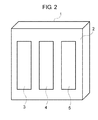
- FIG. 2 shows one example of a light-emitting member in which the phosphor formed using the phosphor material of the present invention is arranged on the base member.
- FIG. 2 shows a configuration of one pixel of a fluorescence film, where reference numeral 1 denotes a base member, 2 denotes a light absorption layer of black matrix etc. and 3 to 5 denote phosphors having different light emission peak wavelengths from each other.
- a red phosphor 3 having a light emission peak wavelength in a wavelength region of 620 nm to 780 nm, a blue phosphor 4 having a light emission peak wavelength in a wavelength region of 435 nm to 480 nm, and a phosphor 5 formed using the phosphor material of the present invention are at least arranged on the base member 1 to form a light-emitting member including phosphor regions of three colors.
- the order and the arrangement of the phosphor region are not limited to the above arrangement.
- the light-emitting member of the present invention may be formed with a phosphor region of one color of only the phosphor 5.
- the light-emitting member of the present invention may be formed with phosphor regions of four or more colors if necessary to realize a higher luminance display having wide color gamut.
- the light-emitting member described above may also include an electrode to be applied with a predetermined potential.
- the electrode includes aluminum and ITO, and is formed through vapor deposition method and sputtering method.
- Y 2 O 2 S:Eu (red), CaS:Eu (red), ZnS:Ag, Al (blue), CaMgSi 2 O 6 :Eu (blue) etc. may be appropriately combined and used according to the display characteristics of the light-emitting member.
- the display color gamut enhances by about 7% compared to the combination of three colors of the above red and blue phosphors, and green phosphor SrGa 2 S 4 :Eu conventionally used.
- Ba 0.1 Sr 0.9 Ga 2 S 4 :Eu obtains higher luminance than SrGa 2 S 4 :Eu.
- the optimum composition ratio can be selected according to the combination of the phosphor materials of the other two colors to be used and the required luminance characteristic, and is preferably selected from 0.03 ⁇ X ⁇ 0.4.
- FIG. 3 is a cross sectional view.
- FIG. 5 is a perspective view partially cutout to show the internal configuration.
- reference numeral 2 denotes a black matrix
- 3, 4, 5 denote phosphor materials
- 9 denotes a cathode electrode
- 10 denotes an insulating layer
- 11 denotes a gate electrode
- 12 denotes an opening of the insulating layer
- 13 denotes an electron-emitting portion
- 14 denotes a substrate (face plate 21 side)
- 19 denotes a metal back
- 21 denotes a face plate.
- 8 denotes a substrate (rear plate 20 side)
- 23 denotes an electron-emitting region
- 24 denotes a supporting frame.
- FIGS. 3 and 5 uses a Spindt type electron-emitting device as an excitation source.
- a configuration of one device is shown in FIG. 4 .
- the reference numerals in FIG. 4 are the same as in FIGS. 3 and 5 .
- An optimum FED including MIM type or surface conduction type can be selected other than the Spindt type.
- FIGS. 7A and 7B show a configuration of the surface conduction electron-emitting device
- FIG. 8 shows a schematic configuration of a panel of the image display apparatus of the present invention using the same.
- FIG. 8 is a perspective view partially cutout to show the internal configuration.
- reference numeral 51 denotes a substrate
- 52 denote device electrodes
- 54 denotes a conductive film
- 55 denotes an electron-emitting portion
- 62 denotes a fixing member
- 63 denotes a spacer
- 64 denotes a X-direction wiring
- 65 denotes a Y-direction wiring
- 66 denotes an electron-emitting device, where same reference numerals are denoted for members same as in FIG. 5 .
- a phosphor material of the present invention was produced.
- Strontium sulfide powder (SrS), barium sulfide powder (BaS), gallium sulfide powder (Ga 2 S 3 ), and europium chloride powder (EuCl 3 ) were used as the material, and the respective powders were mixed using a mortar.
- the respective materials were weighed to meet the weight ratio of SrS:BaS:Ga 2 S 3 :EuCl 3 ⁇ 0.44:0.09:1:0.03 so that the host material has a composition represented by Ba 0.1 Sr 0.9 Ga 2 S 4 .
- the concentration of Eu was three atomic percent with respect to the molar concentration of Sr + Ba.
- the powder was then put into a crucible made of alumina, arranged in an atmosphere of hydrogen sulfide gas diluted with argon to 2%, and subjected to a crystallizing process in the atmosphere of 1000°C for two hours.
- Luminance obtained by irradiating 0.1 gram powder with the electron beam having a current density of 1 mA/cm 2 was 454 cd/m 2 . This luminance is approximately 1.30 times as high as that of the phosphor SrGa 2 S 4 :Eu produced at the same conditions.
- a phosphor material different in composition ratio was produced through the same process as in Example 1.
- Strontium sulfide powder (SrS), barium sulfide powder (BaS), gallium sulfide powder (Ga 2 S 3 ), and europium chloride powder (EuCl 3 ) were used as the material.
- the materials were weighed to meet the weight ration of SrS:BaS:Ga 2 S 3 :EuCl 3 ⁇ 0.30:0.28:1:0.03 so that the host material has a composition represented by Ba 0.4 Sr 0.6 Ga 2 S 4 .
- Luminance obtained by irradiating 0.1 gram of powder with electron beam having a current density of 1 mA/cm 2 was 363 cd/m 2 . This luminance is approximately 1.04 times as high as that of the SrGa 2 S 4 :Eu phosphor.
- An image display apparatus was produced using the phosphor material produced in Example 1.
- the image display apparatus of the present example is the FED of FIG. 3 equipped with the device whose configuration is shown in FIG. 4 .
- a 200 nm aluminum as the cathode electrode 9 was deposited on the glass substrate 8 by the sputtering method.
- a 600 nm of silicon dioxide was then deposited as the insulating layer 10 by the CVD method, and 100 nm of titanium film was deposited as the gate electrode 11 by the sputtering method.
- the opening 12 with a diameter of 1 ⁇ m was formed in the gate electrode 11 and the insulating layer 10 by photolithography and etching process.
- the substrate passed through the above production process was arranged in the sputtering device, the air in the device was evacuated and then molybdenum was deposited obliquely to form the electron-emitting portion 13 while the substrate 8 was being rotated. Subsequently, the unwanted molybdenum was removed by lift-off to form the electron-emitting portion 13.
- the rear plate 20 was formed by the above process. Description has been made of an area corresponding to one pixel, but actually, such configurations are arranged on the substrate in a matrix form.
- a method of producing a face plate (fluorescent surface) 21 will now be described.
- the black matrix 2 was formed on the glass substrate 14 (base member) by screen printing method to remove unnecessary light-emitting surface. An aperture was formed in a region to be formed with the phosphors 3, 4, 5 shown in FIG. 2 .
- the powder of the phosphor material was dispersed in a binder etc. to form a paste, and the paste was applied to the aperture by screen printing method to form the fluorescent surface.
- the phosphor material used in this case is Y 2 O 2 S : Eu to form the red phosphor 3, ZnS:Ag, Cl to form the blue phosphor 4, and Ba 0.1 Sr 0.9 Ga 2 S 4 : Eu to form the phosphor 5.
- Ba 0.1 Sr 0.9 Ga 2 S 4 : Eu was produced at the same conditions as in Example 1.
- a 100 nm aluminum as the metal back 19 was deposited through an evaporation method to form the face plate 21. Description has been made of an area corresponding to one pixel, but actually, such configurations are arranged on the substrate in a matrix form.
- the rear plate 20 and the face plate 21 produced in the above manner were combined to produce the FED.
- the electron-emitting region 23 is arranged in a region where the cathode electrode 9 and the gate electrode 11 cross. Each of the plurality of electron-emitting regions 23 is arranged so as to correspond to each phosphor 3 to 5 shown in FIG. 2 .
- the supporting frame 24 is arranged at the joining part of the rear plate 20 and the face plate 21.
- High voltage terminal Hv is connected to the face plate 21.
- the application voltage is 10kV.
- Signal input terminals Dx1 to Dxm, and Dy1 to Dyn are connected to the cathode electrode 9 and the gate electrode 11, respectively, in the rear plate 20, where a signal from the drive driver is input to the respective terminal.
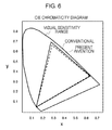
- the display color gamut of the display produced in the above manner is shown in the CIE chromaticity diagram of FIG. 6 .
- the FED of the present invention realized enlargement of the color gamut by about 7% in the display region compared to the FED of the prior art.
- a phosphor of the present invention includes Ba x Sr 1x Ga 2 S 4 :Eu, where 0 ⁇ X ⁇ 0.5. Preferably, 0.03 ⁇ X ⁇ 0.4.
- a light-emitting member of the present invention includes a base member; and a phosphor arranged on the base member.
- An image display apparatus of the present invention includes the light-emitting member and an excitation source for light emitting the light-emitting member.
Landscapes
- Chemical & Material Sciences (AREA)
- Inorganic Chemistry (AREA)
- Engineering & Computer Science (AREA)
- Materials Engineering (AREA)
- Organic Chemistry (AREA)
- Luminescent Compositions (AREA)
- Cathode-Ray Tubes And Fluorescent Screens For Display (AREA)
Applications Claiming Priority (1)
| Application Number | Priority Date | Filing Date | Title |
|---|---|---|---|
| JP2007116151A JP2008274028A (ja) | 2007-04-25 | 2007-04-25 | 蛍光体材料、発光部材および画像形成装置 |
Publications (2)
| Publication Number | Publication Date |
|---|---|
| EP1988145A2 true EP1988145A2 (de) | 2008-11-05 |
| EP1988145A3 EP1988145A3 (de) | 2009-12-16 |
Family
ID=39562013
Family Applications (1)
| Application Number | Title | Priority Date | Filing Date |
|---|---|---|---|
| EP08154520A Withdrawn EP1988145A3 (de) | 2007-04-25 | 2008-04-15 | Phosphor, lichtemittierendes Element und Bilderzeugungsvorrichtung |
Country Status (5)
| Country | Link |
|---|---|
| US (1) | US20080265747A1 (de) |
| EP (1) | EP1988145A3 (de) |
| JP (1) | JP2008274028A (de) |
| KR (1) | KR20080095762A (de) |
| CN (1) | CN101294074A (de) |
Cited By (1)
| Publication number | Priority date | Publication date | Assignee | Title |
|---|---|---|---|---|
| EP2369613A3 (de) * | 2010-03-22 | 2012-05-02 | Samsung Electronics Co., Ltd. | Feldemissionsartige Vorrichtung für Oberflächenlichtquellen und Bildanzeigevorrichtung damit |
Families Citing this family (3)
| Publication number | Priority date | Publication date | Assignee | Title |
|---|---|---|---|---|
| JP2009293022A (ja) * | 2008-05-09 | 2009-12-17 | Mitsui Mining & Smelting Co Ltd | 緑色蛍光体 |
| JP6871098B2 (ja) * | 2017-07-26 | 2021-05-12 | デクセリアルズ株式会社 | 蛍光体、及びその製造方法、蛍光体シート、並びに照明装置 |
| WO2022209033A1 (ja) * | 2021-03-30 | 2022-10-06 | 三井金属鉱業株式会社 | 蛍光体及びその製造方法、蛍光体を含む発光素子並びに発光装置 |
Citations (4)
| Publication number | Priority date | Publication date | Assignee | Title |
|---|---|---|---|---|
| US3639254A (en) | 1969-07-01 | 1972-02-01 | Gte Laboratories Inc | Alkaline earth thiogallate phosphors |
| JPS6038431B2 (ja) | 1977-01-24 | 1985-08-31 | 大日本塗料株式会社 | カラ−ブラウン管 |
| JP2007036041A (ja) | 2005-07-28 | 2007-02-08 | Sony Corp | 発光装置及び光学装置 |
| US20070090748A1 (en) | 2005-10-24 | 2007-04-26 | Canon Kabushiki Kaisha | Phosphor material, light emitting member and image display apparatus using the same |
Family Cites Families (7)
| Publication number | Priority date | Publication date | Assignee | Title |
|---|---|---|---|---|
| EP0887833B1 (de) * | 1997-05-22 | 2006-08-16 | Hitachi Chemical Co., Ltd. | Verfahren zur Herstellung eines Phosphormusters für eine Feldemissionsanzeigetafel und photoempfindliches Element |
| US6580097B1 (en) * | 1998-02-06 | 2003-06-17 | General Electric Company | Light emitting device with phosphor composition |
| KR100342044B1 (ko) * | 1999-04-14 | 2002-06-27 | 김순택 | 녹색발광 형광체 조성물 및 이를 이용하여 제조된 음극선관 |
| DE10051242A1 (de) * | 2000-10-17 | 2002-04-25 | Philips Corp Intellectual Pty | Lichtemittierende Vorrichtung mit beschichtetem Leuchtstoff |
| JP2007056235A (ja) * | 2005-07-28 | 2007-03-08 | Sony Corp | 蛍光体、光学装置、及び表示装置 |
| JP2007335399A (ja) * | 2006-05-19 | 2007-12-27 | Canon Inc | 画像表示装置及び画像表示装置の駆動方法 |
| CN101294075A (zh) * | 2007-04-23 | 2008-10-29 | 三星Sdi株式会社 | 绿色荧光粉、含其的发光器件及包括该器件的液晶显示器 |
-
2007
- 2007-04-25 JP JP2007116151A patent/JP2008274028A/ja not_active Withdrawn
-
2008
- 2008-03-27 US US12/056,447 patent/US20080265747A1/en not_active Abandoned
- 2008-04-15 EP EP08154520A patent/EP1988145A3/de not_active Withdrawn
- 2008-04-15 KR KR1020080034518A patent/KR20080095762A/ko not_active Ceased
- 2008-04-25 CN CNA200810096002XA patent/CN101294074A/zh active Pending
Patent Citations (5)
| Publication number | Priority date | Publication date | Assignee | Title |
|---|---|---|---|---|
| US3639254A (en) | 1969-07-01 | 1972-02-01 | Gte Laboratories Inc | Alkaline earth thiogallate phosphors |
| JPS6038431B2 (ja) | 1977-01-24 | 1985-08-31 | 大日本塗料株式会社 | カラ−ブラウン管 |
| JP2007036041A (ja) | 2005-07-28 | 2007-02-08 | Sony Corp | 発光装置及び光学装置 |
| US20070090748A1 (en) | 2005-10-24 | 2007-04-26 | Canon Kabushiki Kaisha | Phosphor material, light emitting member and image display apparatus using the same |
| JP2007112950A (ja) | 2005-10-24 | 2007-05-10 | Canon Inc | 蛍光体材料及びこれを用いた発光部材、画像表示装置 |
Cited By (2)
| Publication number | Priority date | Publication date | Assignee | Title |
|---|---|---|---|---|
| EP2369613A3 (de) * | 2010-03-22 | 2012-05-02 | Samsung Electronics Co., Ltd. | Feldemissionsartige Vorrichtung für Oberflächenlichtquellen und Bildanzeigevorrichtung damit |
| US8558444B2 (en) | 2010-03-22 | 2013-10-15 | Samsung Electronics Co., Ltd. | Field emission type surface light source device and image display apparatus employing the same |
Also Published As
| Publication number | Publication date |
|---|---|
| JP2008274028A (ja) | 2008-11-13 |
| KR20080095762A (ko) | 2008-10-29 |
| CN101294074A (zh) | 2008-10-29 |
| EP1988145A3 (de) | 2009-12-16 |
| US20080265747A1 (en) | 2008-10-30 |
Similar Documents
| Publication | Publication Date | Title |
|---|---|---|
| KR100489575B1 (ko) | 표시 장치용 형광체 및 그것을 이용한 전계 방출형 표시장치 | |
| EP1995295A1 (de) | Leuchtstoff für display und feldemissionsdisplay | |
| US20070090748A1 (en) | Phosphor material, light emitting member and image display apparatus using the same | |
| EP1988145A2 (de) | Phosphor, lichtemittierendes Element und Bilderzeugungsvorrichtung | |
| US7525245B2 (en) | Electron beam excited fluorescence emitting device | |
| KR100502877B1 (ko) | 화상 표시 장치 | |
| KR100821047B1 (ko) | 청색 형광체 및 그것을 이용한 디스플레이패널 | |
| JP2002226847A (ja) | 表示装置用蛍光体およびそれを用いた電界放出型表示装置 | |
| KR100676352B1 (ko) | 표시 장치용 형광체와 그의 제조 방법, 및 그를 이용한컬러 표시 장치 | |
| JP2004123786A (ja) | 表示装置用蛍光体とその製造方法、およびそれを用いたカラー表示装置 | |
| JP4077131B2 (ja) | フルカラー薄膜elディスプレイパネル | |
| US20060145591A1 (en) | Green light emitting phosphor for low voltage/high current density and field emission type display including the same | |
| US20080265742A1 (en) | Display Unit-Use Blue Light Emitting Fluorescent Substance and Production Method Therefor and Field Emission Type Display Unit | |
| JP5119631B2 (ja) | 画像表示装置 | |
| US7400099B2 (en) | Flat panel image display device | |
| US20080265743A1 (en) | Green Light-Emitting Phosphor for Displays and Field-Emission Display Using Same | |
| JP2004339293A (ja) | 低電圧・高電流密度用青色発光蛍光体とそれを用いた電界放出型表示装置 | |
| JP2004123787A (ja) | 表示装置用蛍光体とそれを用いたカラー表示装置 | |
| JP2008140617A (ja) | 赤色発光素子および電界放出型表示装置 | |
| JP2007177078A (ja) | 表示装置用蛍光体および電界放出型表示装置 | |
| WO2006051601A1 (ja) | 表示装置用蛍光体とその製造方法、およびそれを用いた電界放射型表示装置 | |
| JP2008130305A (ja) | 緑色発光素子および電界放出型表示装置 |
Legal Events
| Date | Code | Title | Description |
|---|---|---|---|
| PUAI | Public reference made under article 153(3) epc to a published international application that has entered the european phase |
Free format text: ORIGINAL CODE: 0009012 |
|
| AK | Designated contracting states |
Kind code of ref document: A2 Designated state(s): AT BE BG CH CY CZ DE DK EE ES FI FR GB GR HR HU IE IS IT LI LT LU LV MC MT NL NO PL PT RO SE SI SK TR |
|
| AX | Request for extension of the european patent |
Extension state: AL BA MK RS |
|
| PUAL | Search report despatched |
Free format text: ORIGINAL CODE: 0009013 |
|
| AK | Designated contracting states |
Kind code of ref document: A3 Designated state(s): AT BE BG CH CY CZ DE DK EE ES FI FR GB GR HR HU IE IS IT LI LT LU LV MC MT NL NO PL PT RO SE SI SK TR |
|
| AX | Request for extension of the european patent |
Extension state: AL BA MK RS |
|
| 17P | Request for examination filed |
Effective date: 20100616 |
|
| AKX | Designation fees paid |
Designated state(s): DE FR GB |
|
| 17Q | First examination report despatched |
Effective date: 20101109 |
|
| STAA | Information on the status of an ep patent application or granted ep patent |
Free format text: STATUS: THE APPLICATION HAS BEEN WITHDRAWN |
|
| 18W | Application withdrawn |
Effective date: 20111019 |