EP1988187A2 - Appareil et procédé permettant de réduire le taux d'érosion des surfaces exposées aux plasmas contenant de l'halogène - Google Patents
Appareil et procédé permettant de réduire le taux d'érosion des surfaces exposées aux plasmas contenant de l'halogène Download PDFInfo
- Publication number
- EP1988187A2 EP1988187A2 EP08154940A EP08154940A EP1988187A2 EP 1988187 A2 EP1988187 A2 EP 1988187A2 EP 08154940 A EP08154940 A EP 08154940A EP 08154940 A EP08154940 A EP 08154940A EP 1988187 A2 EP1988187 A2 EP 1988187A2
- Authority
- EP
- European Patent Office
- Prior art keywords
- mole
- oxide
- ceramic
- concentration ranging
- molar concentration
- Prior art date
- Legal status (The legal status is an assumption and is not a legal conclusion. Google has not performed a legal analysis and makes no representation as to the accuracy of the status listed.)
- Withdrawn
Links
- 210000002381 plasma Anatomy 0.000 title claims abstract description 128
- 230000003628 erosive effect Effects 0.000 title claims abstract description 108
- 229910052736 halogen Inorganic materials 0.000 title claims abstract description 21
- 150000002367 halogens Chemical class 0.000 title claims abstract description 21
- 238000000034 method Methods 0.000 title claims description 91
- 239000000919 ceramic Substances 0.000 claims abstract description 148
- SIWVEOZUMHYXCS-UHFFFAOYSA-N oxo(oxoyttriooxy)yttrium Chemical compound O=[Y]O[Y]=O SIWVEOZUMHYXCS-UHFFFAOYSA-N 0.000 claims abstract description 136
- 238000012545 processing Methods 0.000 claims abstract description 105
- TWNQGVIAIRXVLR-UHFFFAOYSA-N oxo(oxoalumanyloxy)alumane Chemical compound O=[Al]O[Al]=O TWNQGVIAIRXVLR-UHFFFAOYSA-N 0.000 claims abstract description 104
- RVTZCBVAJQQJTK-UHFFFAOYSA-N oxygen(2-);zirconium(4+) Chemical compound [O-2].[O-2].[Zr+4] RVTZCBVAJQQJTK-UHFFFAOYSA-N 0.000 claims abstract description 96
- 229910001928 zirconium oxide Inorganic materials 0.000 claims abstract description 96
- 239000004065 semiconductor Substances 0.000 claims abstract description 81
- VQCBHWLJZDBHOS-UHFFFAOYSA-N erbium(iii) oxide Chemical compound O=[Er]O[Er]=O VQCBHWLJZDBHOS-UHFFFAOYSA-N 0.000 claims abstract description 20
- PLDDOISOJJCEMH-UHFFFAOYSA-N neodymium(3+);oxygen(2-) Chemical compound [O-2].[O-2].[O-2].[Nd+3].[Nd+3] PLDDOISOJJCEMH-UHFFFAOYSA-N 0.000 claims abstract description 20
- HYXGAEYDKFCVMU-UHFFFAOYSA-N scandium oxide Chemical compound O=[Sc]O[Sc]=O HYXGAEYDKFCVMU-UHFFFAOYSA-N 0.000 claims abstract description 12
- FKTOIHSPIPYAPE-UHFFFAOYSA-N samarium(iii) oxide Chemical compound [O-2].[O-2].[O-2].[Sm+3].[Sm+3] FKTOIHSPIPYAPE-UHFFFAOYSA-N 0.000 claims abstract description 11
- 229910000420 cerium oxide Inorganic materials 0.000 claims abstract description 9
- 229910000449 hafnium oxide Inorganic materials 0.000 claims abstract description 9
- WIHZLLGSGQNAGK-UHFFFAOYSA-N hafnium(4+);oxygen(2-) Chemical compound [O-2].[O-2].[Hf+4] WIHZLLGSGQNAGK-UHFFFAOYSA-N 0.000 claims abstract description 9
- 229910000484 niobium oxide Inorganic materials 0.000 claims abstract description 9
- URLJKFSTXLNXLG-UHFFFAOYSA-N niobium(5+);oxygen(2-) Chemical compound [O-2].[O-2].[O-2].[O-2].[O-2].[Nb+5].[Nb+5] URLJKFSTXLNXLG-UHFFFAOYSA-N 0.000 claims abstract description 9
- BMMGVYCKOGBVEV-UHFFFAOYSA-N oxo(oxoceriooxy)cerium Chemical compound [Ce]=O.O=[Ce]=O BMMGVYCKOGBVEV-UHFFFAOYSA-N 0.000 claims abstract description 9
- UZLYXNNZYFBAQO-UHFFFAOYSA-N oxygen(2-);ytterbium(3+) Chemical compound [O-2].[O-2].[O-2].[Yb+3].[Yb+3] UZLYXNNZYFBAQO-UHFFFAOYSA-N 0.000 claims abstract description 9
- 229910001954 samarium oxide Inorganic materials 0.000 claims abstract description 9
- 229940075630 samarium oxide Drugs 0.000 claims abstract description 9
- 229910003454 ytterbium oxide Inorganic materials 0.000 claims abstract description 9
- 229940075624 ytterbium oxide Drugs 0.000 claims abstract description 9
- 230000008569 process Effects 0.000 claims description 52
- 239000000758 substrate Substances 0.000 claims description 50
- 239000007787 solid Substances 0.000 claims description 26
- 238000009826 distribution Methods 0.000 claims description 18
- 229910000838 Al alloy Inorganic materials 0.000 claims description 15
- 239000006104 solid solution Substances 0.000 description 75
- 239000000203 mixture Substances 0.000 description 34
- RUDFQVOCFDJEEF-UHFFFAOYSA-N yttrium(III) oxide Inorganic materials [O-2].[O-2].[O-2].[Y+3].[Y+3] RUDFQVOCFDJEEF-UHFFFAOYSA-N 0.000 description 29
- MCMNRKCIXSYSNV-UHFFFAOYSA-N Zirconium dioxide Chemical compound O=[Zr]=O MCMNRKCIXSYSNV-UHFFFAOYSA-N 0.000 description 23
- 239000007789 gas Substances 0.000 description 23
- 229910052751 metal Inorganic materials 0.000 description 23
- 239000002184 metal Substances 0.000 description 23
- PNEYBMLMFCGWSK-UHFFFAOYSA-N aluminium oxide Inorganic materials [O-2].[O-2].[O-2].[Al+3].[Al+3] PNEYBMLMFCGWSK-UHFFFAOYSA-N 0.000 description 22
- 239000002131 composite material Substances 0.000 description 22
- 239000011248 coating agent Substances 0.000 description 21
- 238000000576 coating method Methods 0.000 description 21
- 238000012360 testing method Methods 0.000 description 19
- 238000005530 etching Methods 0.000 description 18
- 239000000463 material Substances 0.000 description 18
- 229910052782 aluminium Inorganic materials 0.000 description 17
- XAGFODPZIPBFFR-UHFFFAOYSA-N aluminium Chemical compound [Al] XAGFODPZIPBFFR-UHFFFAOYSA-N 0.000 description 17
- 229910010293 ceramic material Inorganic materials 0.000 description 17
- 229910052593 corundum Inorganic materials 0.000 description 16
- 229910001845 yogo sapphire Inorganic materials 0.000 description 16
- 239000010410 layer Substances 0.000 description 14
- 229910052574 oxide ceramic Inorganic materials 0.000 description 14
- 239000011224 oxide ceramic Substances 0.000 description 14
- 229910052727 yttrium Inorganic materials 0.000 description 14
- 239000013078 crystal Substances 0.000 description 13
- VWQVUPCCIRVNHF-UHFFFAOYSA-N yttrium atom Chemical compound [Y] VWQVUPCCIRVNHF-UHFFFAOYSA-N 0.000 description 12
- XPDWGBQVDMORPB-UHFFFAOYSA-N Fluoroform Chemical compound FC(F)F XPDWGBQVDMORPB-UHFFFAOYSA-N 0.000 description 11
- JNDMLEXHDPKVFC-UHFFFAOYSA-N aluminum;oxygen(2-);yttrium(3+) Chemical compound [O-2].[O-2].[O-2].[Al+3].[Y+3] JNDMLEXHDPKVFC-UHFFFAOYSA-N 0.000 description 10
- 239000000843 powder Substances 0.000 description 10
- 239000011247 coating layer Substances 0.000 description 9
- 238000004519 manufacturing process Methods 0.000 description 8
- 239000011253 protective coating Substances 0.000 description 8
- 239000007858 starting material Substances 0.000 description 7
- 230000015572 biosynthetic process Effects 0.000 description 6
- 150000001875 compounds Chemical class 0.000 description 6
- 230000007797 corrosion Effects 0.000 description 6
- 238000005260 corrosion Methods 0.000 description 6
- 229910052731 fluorine Inorganic materials 0.000 description 6
- 238000005245 sintering Methods 0.000 description 6
- YCKRFDGAMUMZLT-UHFFFAOYSA-N Fluorine atom Chemical compound [F] YCKRFDGAMUMZLT-UHFFFAOYSA-N 0.000 description 5
- VYPSYNLAJGMNEJ-UHFFFAOYSA-N Silicium dioxide Chemical compound O=[Si]=O VYPSYNLAJGMNEJ-UHFFFAOYSA-N 0.000 description 5
- 239000011230 binding agent Substances 0.000 description 5
- 210000004027 cell Anatomy 0.000 description 5
- 239000011737 fluorine Substances 0.000 description 5
- 230000006872 improvement Effects 0.000 description 5
- 229910052760 oxygen Inorganic materials 0.000 description 5
- QVGXLLKOCUKJST-UHFFFAOYSA-N atomic oxygen Chemical compound [O] QVGXLLKOCUKJST-UHFFFAOYSA-N 0.000 description 4
- 238000005229 chemical vapour deposition Methods 0.000 description 4
- 238000004140 cleaning Methods 0.000 description 4
- 238000009694 cold isostatic pressing Methods 0.000 description 4
- 238000011109 contamination Methods 0.000 description 4
- 230000007547 defect Effects 0.000 description 4
- ZKATWMILCYLAPD-UHFFFAOYSA-N niobium pentoxide Chemical compound O=[Nb](=O)O[Nb](=O)=O ZKATWMILCYLAPD-UHFFFAOYSA-N 0.000 description 4
- 239000001301 oxygen Substances 0.000 description 4
- NYWITVDHYCKDAU-UHFFFAOYSA-N oxygen(2-) yttrium(3+) zirconium(4+) Chemical compound [O--].[O--].[Y+3].[Zr+4] NYWITVDHYCKDAU-UHFFFAOYSA-N 0.000 description 4
- 238000003825 pressing Methods 0.000 description 4
- 238000001694 spray drying Methods 0.000 description 4
- 229910019901 yttrium aluminum garnet Inorganic materials 0.000 description 4
- 229910052684 Cerium Inorganic materials 0.000 description 3
- KDBCKQIMMRZEBB-UHFFFAOYSA-N aluminum oxygen(2-) yttrium(3+) zirconium(4+) Chemical compound [O-2].[Al+3].[O-2].[Zr+4].[O-2].[Y+3] KDBCKQIMMRZEBB-UHFFFAOYSA-N 0.000 description 3
- 238000005524 ceramic coating Methods 0.000 description 3
- 238000004814 ceramic processing Methods 0.000 description 3
- 230000000052 comparative effect Effects 0.000 description 3
- PMHQVHHXPFUNSP-UHFFFAOYSA-M copper(1+);methylsulfanylmethane;bromide Chemical compound Br[Cu].CSC PMHQVHHXPFUNSP-UHFFFAOYSA-M 0.000 description 3
- 238000005516 engineering process Methods 0.000 description 3
- 238000009472 formulation Methods 0.000 description 3
- 239000012535 impurity Substances 0.000 description 3
- 239000002245 particle Substances 0.000 description 3
- 239000011241 protective layer Substances 0.000 description 3
- 239000010453 quartz Substances 0.000 description 3
- 229910052706 scandium Inorganic materials 0.000 description 3
- HBMJWWWQQXIZIP-UHFFFAOYSA-N silicon carbide Chemical compound [Si+]#[C-] HBMJWWWQQXIZIP-UHFFFAOYSA-N 0.000 description 3
- 229910010271 silicon carbide Inorganic materials 0.000 description 3
- 238000004088 simulation Methods 0.000 description 3
- 239000010935 stainless steel Substances 0.000 description 3
- 229910001220 stainless steel Inorganic materials 0.000 description 3
- 230000003746 surface roughness Effects 0.000 description 3
- 229910017083 AlN Inorganic materials 0.000 description 2
- IJGRMHOSHXDMSA-UHFFFAOYSA-N Atomic nitrogen Chemical compound N#N IJGRMHOSHXDMSA-UHFFFAOYSA-N 0.000 description 2
- 229910052692 Dysprosium Inorganic materials 0.000 description 2
- 229910052693 Europium Inorganic materials 0.000 description 2
- KRHYYFGTRYWZRS-UHFFFAOYSA-M Fluoride anion Chemical compound [F-] KRHYYFGTRYWZRS-UHFFFAOYSA-M 0.000 description 2
- CETPSERCERDGAM-UHFFFAOYSA-N ceric oxide Chemical compound O=[Ce]=O CETPSERCERDGAM-UHFFFAOYSA-N 0.000 description 2
- 229910000421 cerium(III) oxide Inorganic materials 0.000 description 2
- 229910000422 cerium(IV) oxide Inorganic materials 0.000 description 2
- 239000003795 chemical substances by application Substances 0.000 description 2
- 239000000356 contaminant Substances 0.000 description 2
- 238000001816 cooling Methods 0.000 description 2
- 230000000694 effects Effects 0.000 description 2
- CJNBYAVZURUTKZ-UHFFFAOYSA-N hafnium(IV) oxide Inorganic materials O=[Hf]=O CJNBYAVZURUTKZ-UHFFFAOYSA-N 0.000 description 2
- 229910052746 lanthanum Inorganic materials 0.000 description 2
- 238000002156 mixing Methods 0.000 description 2
- 229910052757 nitrogen Inorganic materials 0.000 description 2
- 238000007750 plasma spraying Methods 0.000 description 2
- 238000001272 pressureless sintering Methods 0.000 description 2
- 230000009257 reactivity Effects 0.000 description 2
- 239000000126 substance Substances 0.000 description 2
- FIXNOXLJNSSSLJ-UHFFFAOYSA-N ytterbium(III) oxide Inorganic materials O=[Yb]O[Yb]=O FIXNOXLJNSSSLJ-UHFFFAOYSA-N 0.000 description 2
- OMQSJNWFFJOIMO-UHFFFAOYSA-J zirconium tetrafluoride Chemical compound F[Zr](F)(F)F OMQSJNWFFJOIMO-UHFFFAOYSA-J 0.000 description 2
- 229910052580 B4C Inorganic materials 0.000 description 1
- 229910015844 BCl3 Inorganic materials 0.000 description 1
- 229910052582 BN Inorganic materials 0.000 description 1
- 208000010392 Bone Fractures Diseases 0.000 description 1
- PZNSFCLAULLKQX-UHFFFAOYSA-N Boron nitride Chemical compound N#B PZNSFCLAULLKQX-UHFFFAOYSA-N 0.000 description 1
- 206010017076 Fracture Diseases 0.000 description 1
- UFHFLCQGNIYNRP-UHFFFAOYSA-N Hydrogen Chemical compound [H][H] UFHFLCQGNIYNRP-UHFFFAOYSA-N 0.000 description 1
- 229910052581 Si3N4 Inorganic materials 0.000 description 1
- NRTOMJZYCJJWKI-UHFFFAOYSA-N Titanium nitride Chemical compound [Ti]#N NRTOMJZYCJJWKI-UHFFFAOYSA-N 0.000 description 1
- 229910000946 Y alloy Inorganic materials 0.000 description 1
- 239000000654 additive Substances 0.000 description 1
- 230000000996 additive effect Effects 0.000 description 1
- 238000002048 anodisation reaction Methods 0.000 description 1
- 239000006117 anti-reflective coating Substances 0.000 description 1
- INAHAJYZKVIDIZ-UHFFFAOYSA-N boron carbide Chemical compound B12B3B4C32B41 INAHAJYZKVIDIZ-UHFFFAOYSA-N 0.000 description 1
- 229910052794 bromium Inorganic materials 0.000 description 1
- GWXLDORMOJMVQZ-UHFFFAOYSA-N cerium Chemical compound [Ce] GWXLDORMOJMVQZ-UHFFFAOYSA-N 0.000 description 1
- 230000008859 change Effects 0.000 description 1
- 239000003153 chemical reaction reagent Substances 0.000 description 1
- 229910052801 chlorine Inorganic materials 0.000 description 1
- 229910052681 coesite Inorganic materials 0.000 description 1
- 238000007906 compression Methods 0.000 description 1
- 230000006835 compression Effects 0.000 description 1
- 238000007596 consolidation process Methods 0.000 description 1
- 229910052906 cristobalite Inorganic materials 0.000 description 1
- 230000003247 decreasing effect Effects 0.000 description 1
- -1 etc.) Chemical compound 0.000 description 1
- 238000011156 evaluation Methods 0.000 description 1
- 238000010285 flame spraying Methods 0.000 description 1
- 150000002222 fluorine compounds Chemical class 0.000 description 1
- 235000011194 food seasoning agent Nutrition 0.000 description 1
- 239000002241 glass-ceramic Substances 0.000 description 1
- 239000001257 hydrogen Substances 0.000 description 1
- 229910052739 hydrogen Inorganic materials 0.000 description 1
- 150000002500 ions Chemical class 0.000 description 1
- 229910001092 metal group alloy Inorganic materials 0.000 description 1
- 229910003465 moissanite Inorganic materials 0.000 description 1
- WHOPEPSOPUIRQQ-UHFFFAOYSA-N oxoaluminum Chemical compound O1[Al]O[Al]1 WHOPEPSOPUIRQQ-UHFFFAOYSA-N 0.000 description 1
- 230000000149 penetrating effect Effects 0.000 description 1
- 230000035515 penetration Effects 0.000 description 1
- 230000000737 periodic effect Effects 0.000 description 1
- 238000005240 physical vapour deposition Methods 0.000 description 1
- 238000002294 plasma sputter deposition Methods 0.000 description 1
- 238000000623 plasma-assisted chemical vapour deposition Methods 0.000 description 1
- 230000002035 prolonged effect Effects 0.000 description 1
- 230000001681 protective effect Effects 0.000 description 1
- 229910001404 rare earth metal oxide Inorganic materials 0.000 description 1
- 238000012552 review Methods 0.000 description 1
- SIXSYDAISGFNSX-UHFFFAOYSA-N scandium atom Chemical compound [Sc] SIXSYDAISGFNSX-UHFFFAOYSA-N 0.000 description 1
- 230000035939 shock Effects 0.000 description 1
- 238000004904 shortening Methods 0.000 description 1
- 239000000377 silicon dioxide Substances 0.000 description 1
- HQVNEWCFYHHQES-UHFFFAOYSA-N silicon nitride Chemical compound N12[Si]34N5[Si]62N3[Si]51N64 HQVNEWCFYHHQES-UHFFFAOYSA-N 0.000 description 1
- 239000000243 solution Substances 0.000 description 1
- 239000007921 spray Substances 0.000 description 1
- 238000005507 spraying Methods 0.000 description 1
- 229910052682 stishovite Inorganic materials 0.000 description 1
- 238000007751 thermal spraying Methods 0.000 description 1
- FAQYAMRNWDIXMY-UHFFFAOYSA-N trichloroborane Chemical compound ClB(Cl)Cl FAQYAMRNWDIXMY-UHFFFAOYSA-N 0.000 description 1
- 229910052905 tridymite Inorganic materials 0.000 description 1
- 229940105963 yttrium fluoride Drugs 0.000 description 1
- RBORBHYCVONNJH-UHFFFAOYSA-K yttrium(iii) fluoride Chemical compound F[Y](F)F RBORBHYCVONNJH-UHFFFAOYSA-K 0.000 description 1
Images




Classifications
-
- C—CHEMISTRY; METALLURGY
- C04—CEMENTS; CONCRETE; ARTIFICIAL STONE; CERAMICS; REFRACTORIES
- C04B—LIME, MAGNESIA; SLAG; CEMENTS; COMPOSITIONS THEREOF, e.g. MORTARS, CONCRETE OR LIKE BUILDING MATERIALS; ARTIFICIAL STONE; CERAMICS; REFRACTORIES; TREATMENT OF NATURAL STONE
- C04B35/00—Shaped ceramic products characterised by their composition; Ceramics compositions; Processing powders of inorganic compounds preparatory to the manufacturing of ceramic products
- C04B35/50—Shaped ceramic products characterised by their composition; Ceramics compositions; Processing powders of inorganic compounds preparatory to the manufacturing of ceramic products based on rare-earth compounds
- C04B35/505—Shaped ceramic products characterised by their composition; Ceramics compositions; Processing powders of inorganic compounds preparatory to the manufacturing of ceramic products based on rare-earth compounds based on yttrium oxide
-
- C—CHEMISTRY; METALLURGY
- C23—COATING METALLIC MATERIAL; COATING MATERIAL WITH METALLIC MATERIAL; CHEMICAL SURFACE TREATMENT; DIFFUSION TREATMENT OF METALLIC MATERIAL; COATING BY VACUUM EVAPORATION, BY SPUTTERING, BY ION IMPLANTATION OR BY CHEMICAL VAPOUR DEPOSITION, IN GENERAL; INHIBITING CORROSION OF METALLIC MATERIAL OR INCRUSTATION IN GENERAL
- C23C—COATING METALLIC MATERIAL; COATING MATERIAL WITH METALLIC MATERIAL; SURFACE TREATMENT OF METALLIC MATERIAL BY DIFFUSION INTO THE SURFACE, BY CHEMICAL CONVERSION OR SUBSTITUTION; COATING BY VACUUM EVAPORATION, BY SPUTTERING, BY ION IMPLANTATION OR BY CHEMICAL VAPOUR DEPOSITION, IN GENERAL
- C23C16/00—Chemical coating by decomposition of gaseous compounds, without leaving reaction products of surface material in the coating, i.e. chemical vapour deposition [CVD] processes
- C23C16/44—Chemical coating by decomposition of gaseous compounds, without leaving reaction products of surface material in the coating, i.e. chemical vapour deposition [CVD] processes characterised by the method of coating
- C23C16/4401—Means for minimising impurities, e.g. dust, moisture or residual gas, in the reaction chamber
- C23C16/4404—Coatings or surface treatment on the inside of the reaction chamber or on parts thereof
-
- C—CHEMISTRY; METALLURGY
- C04—CEMENTS; CONCRETE; ARTIFICIAL STONE; CERAMICS; REFRACTORIES
- C04B—LIME, MAGNESIA; SLAG; CEMENTS; COMPOSITIONS THEREOF, e.g. MORTARS, CONCRETE OR LIKE BUILDING MATERIALS; ARTIFICIAL STONE; CERAMICS; REFRACTORIES; TREATMENT OF NATURAL STONE
- C04B35/00—Shaped ceramic products characterised by their composition; Ceramics compositions; Processing powders of inorganic compounds preparatory to the manufacturing of ceramic products
- C04B35/01—Shaped ceramic products characterised by their composition; Ceramics compositions; Processing powders of inorganic compounds preparatory to the manufacturing of ceramic products based on oxide ceramics
- C04B35/48—Shaped ceramic products characterised by their composition; Ceramics compositions; Processing powders of inorganic compounds preparatory to the manufacturing of ceramic products based on oxide ceramics based on zirconium or hafnium oxides, zirconates, zircon or hafnates
-
- H—ELECTRICITY
- H01—ELECTRIC ELEMENTS
- H01J—ELECTRIC DISCHARGE TUBES OR DISCHARGE LAMPS
- H01J37/00—Discharge tubes with provision for introducing objects or material to be exposed to the discharge, e.g. for the purpose of examination or processing thereof
- H01J37/32—Gas-filled discharge tubes
- H01J37/32431—Constructional details of the reactor
- H01J37/32458—Vessel
- H01J37/32467—Material
-
- H—ELECTRICITY
- H01—ELECTRIC ELEMENTS
- H01J—ELECTRIC DISCHARGE TUBES OR DISCHARGE LAMPS
- H01J37/00—Discharge tubes with provision for introducing objects or material to be exposed to the discharge, e.g. for the purpose of examination or processing thereof
- H01J37/32—Gas-filled discharge tubes
- H01J37/32431—Constructional details of the reactor
- H01J37/32458—Vessel
- H01J37/32477—Vessel characterised by the means for protecting vessels or internal parts, e.g. coatings
- H01J37/32495—Means for protecting the vessel against plasma
Definitions
- the present application is related to a series of applications filed by various inventors of the present application, many of the applications relate to the use of a yttrium-oxide comprising ceramic in the form of a coating, to provide a plasma-resistant surface which is useful in semiconductor processing applications.
- the applications include U.S. Application Serial No. 10/075,967 of Sun et al., filed February 14, 2002 , titled: "Yttrium Oxide Based Surface Coating For Semiconductor IC Processing Vacuum Chambers", which issued as U.S. Patent No. 6,776,873 on August 17, 2004 ; U.S. Application Serial No.
- the present invention relates to a specialized yttrium oxide comprising solid solution ceramic which is highly resistant to plasmas in general, particularly resistant to corrosive plasmas of the kind used in the etching of semiconductor substrates.
- Corrosion (including erosion) resistance is a critical property for apparatus components and liners used in semiconductor processing chambers, where corrosive environments are present.
- Example of corrosive plasma environments include plasmas used for cleaning of processing apparatus and plasmas used to etch semiconductor substrates. Plasmas used for plasma-enhanced chemical vapor deposition processes often tend to be corrosive as well. This is especially true where high-energy plasma is present and combined with chemical reactivity to act upon the surface of components present in the environment. The reduced chemical reactivity of an apparatus component surface or of a liner surface is also an important property when corrosive gases alone are in contact with processing apparatus surfaces.
- Process chambers and component apparatus present within processing chambers which are used in the fabrication of electronic devices and micro-electromechanical structures (MEMS) are frequently constructed from aluminum and aluminum alloys. Surfaces of a process chamber and component apparatus present within the chamber are frequently anodized to provide a degree of protection from the corrosive environment. However, the integrity of the anodization layer may be deteriorated by impurities in the aluminum or aluminum alloy, so that corrosion begins to occur early, shortening the life span of the protective coating. Ceramic coatings of various compositions have been used in place of the aluminum oxide layer mentioned above, and have been used over the surface of the anodized layer to improve the protection of the underlying aluminum-based materials. However, current materials used for protective layers deteriorate over time and eventually leave the aluminum alloy subject to attack by the plasma, even though the life span of the protective layer is extended over that of anodized aluminum.
- Yttrium oxide is a ceramic material which has shown considerable promise in the protection of aluminum and aluminum alloy surfaces which are exposed to fluorine-containing plasmas of the kind used in the fabrication of semiconductor devices.
- a yttrium oxide coating has been used and applied over an anodized surface of a high purity aluminum alloy process chamber surface, or a process component surface, to produce excellent corrosion protection (e.g. U.S. Patent Nol. 6,777,873 to Sun et al ., mentioned above).
- the '873 Patent provides a processing chamber component resistant to a plasma including fluorine and oxygen species.
- the processing chamber component typically comprises: a high purity aluminum substrate, where particulates formed from mobile impurities present in the aluminum are carefully controlled to have a particular size distribution; an anodized coating on a surface of the high purity aluminum substrate; and, a protective coating comprising yttrium oxide overlying the anodized coating.
- the protective coating may include aluminum oxide up to about 10 % by weight, and typically comprises 99.95 % by weight or greater yttrium oxide.
- the protective coating is coating typically applied using a method such as spray coating, chemical vapor deposition, or physical vapor deposition.
- the Oehrlein et al. reference further discloses that since aluminum is reactive with a number of plasmas, it is recommended that "aluminum oxide or a coating thereof be disposed on the liner or chamber walls", because aluminum oxide tends to be chemically inert.
- a protective coating may be applied over the surfaces of the liner and/or chamber walls. Examples which are given include Al 2 O 3 , Sc 2 O 3 , or Y 2 O 3 .
- U.S. Patent Application Publication No. US 2001/0003271A1 discloses a film of Al 2 O 3 , or Al 2 O 3 and Y 2 O 3 , formed on an inner wall surface of the chamber and on those exposed surfaces of the members within the chamber which require a high corrosion resistance and insulating property.
- a base material of the chamber may be a ceramic material (Al 2 O 3 , SiO 2 , AlN, etc.), aluminum, or stainless steel, or other metal or metal alloy, which has a sprayed film over the base material.
- the film may be made of a compound of a III-B element of the periodic table, such as Y 2 O 3
- the film may substantially comprise Al 2 O 3 and Y 2 O 3 .
- a sprayed film of yttrium-aluminum-garnet (YAG) is also mentioned.
- the sprayed film thickness is said to range from 50 ⁇ m to 300 ⁇ m.
- a ceramic composition of matter comprising a ceramic compound (e.g. Al 2 O 3 ) and an oxide of a Group IIIB metal (e.g. Y 2 O 3 ) has been used for a dielectric window of a reactor chamber where substrates are processed in a plasma of a processing gas (e.g. U.S. Patent No. 6,352,611, to Han et al., issued March 5, 2002 ).
- the ceramic compound may be selected from silicon carbide, silicon nitride, boron carbide, boron nitride, aluminum nitride, aluminum oxide, and mixtures thereof; however, aluminum oxide is said to be available in a pure form which does not outgas.
- the Group IIIB metal may be selected from the group consisting of scandium, yttrium, the cerium subgroup, and the yttrium subgroup; however, yttrium is preferred, with the oxide being yttrium oxide.
- the preferred process for forming or producing the dielectric member is by thermal processing of a powdered raw mixture comprising the ceramic compound, the oxide of a Group IIIB metal, a suitable additive agent, and a suitable binder agent.
- a protective coating for a semiconductor processing apparatus component comprises aluminum or an aluminum alloy, where the coating includes a material selected from, for example, but not limited to: yttrium-aluminum-garnet (YAG); an oxide of an element selected from the group consisting of Y, Sc, La, Ce, Eu, and Dy; a fluoride of an element selected from the group consisting of Y, Sc, La, Ce, Eu, and Dy; and combinations thereof is used (e.g. U.S. Patent Application Serial No.10/898,113 of Sun et al., filed July 22, 2004 , and entitled "Clean, Dense Yttrium Oxide Coating Protecting Semiconductor Apparatus", mentioned above).
- the coating is applied to a substrate surface by thermal / flame spraying, plasma spraying, sputtering, or chemical vapor deposition (CVD).
- the coating is placed in compression by applying the coating at a substrate surface temperature of at least about 150-200°C.
- the kinds of protective coatings described above have been used to protect exposed surfaces of a plasma source gas distribution plate of the kind used in semiconductor and MEMS processing apparatus.
- the lifetime of the gas distribution plate has typically been limited, from about 8 processing days to about 80 processing days, depending on the corrosivity of the plasma created in the processing chamber.
- a gas distribution plate was fabricated from a solid yttrium oxide-comprising substrate, as described in U.S. Application No. 10/918,232 of Sun et al ., mentioned above.
- the solid yttrium oxide-comprising substrate contains up to about 10 % aluminum oxide in some instances.
- the solid yttrium oxide-comprising substrate typically comprises about 99.99 % yttrium oxide.
- Semiconductor processing conditions expose semiconductor processing apparatus, such as the interior of processing chambers and the surfaces of components within the processing chambers, to a variety of chemical reagents and plasma ions which attack processing apparatus surfaces.
- the effect of the attack on an apparatus surface is frequently referred to as erosion of the apparatus surface. It is possible to reduce the erosion rate by selecting a particular material composition for the apparatus surfaces.
- a protective material may be applied as a coating over the apparatus surface; however, this may not be the best solution to avoiding erosion.
- the coating is constantly getting thinner (eroding) during a plasma etch, and there is an increased risk that the substrate beneath the coating will be attacked by the plasma penetrating the coating layer.
- the coating layer may flake off during plasma processing due to residual stress.
- Embodiments of the present invention pertain to reducing the erosion rate of a ceramic material, typically comprising a Group IIIA, IIIB, IVB, or a Group IVB element, or combinations thereof, while maintaining acceptable mechanical properties or improving mechanical properties of the component parts made of the ceramic material.
- sintered ceramics are formed which contain a single solid solution phase or which are multi-phase, such as two phase and three phase.
- the multi-phase ceramics typically contain a yttrium aluminate phase and one or two solid solution phases formed from yttrium oxide, zirconium oxide and/or rare earth oxides.
- the sintered ceramic has been evaluated under various plasma processing conditions to determine erosion resistance. The materials which were erosion tested were also tested for mechanical properties.
- ceramic materials formed from starting compositions in which the Y 2 O 3 , yttrium oxide, molar concentration ranges from about 50 mole % to about 75 mole %; the ZrO 2 , zirconium oxide, molar concentration ranges from about 10 mole % to about 30 mole %; and, the Al 2 O 3 , aluminum oxide, molar concentration ranges from about 10 mole % to about 30 mole % provide excellent erosion resistance to halogen-containing plasmas while providing advanced mechanical properties which enable handling of solid ceramic processing components with less concern about damage to a component.
- a starting composition for the ceramic materials may be one that comprises Y 2 O 3 molar concentration ranges from about 55 mole % to about 65 mole %, ZrO 2 molar concentration ranges from about 15 mole % to about 25 mole %, and Al 2 O 3 molar concentration ranges from about 10 mole % to about 25 mole %.
- the starting material concentration of the ceramic material may be one that comprises Y 2 O 3 molar concentration ranges from about 55 mole % to about 65 mole %, the ZrO 2 molar concentration ranges from about 20 mole % to about 25 mole % and the Al 2 O 3 molar concentration 10 mole % to about 15 mole %.
- these starting material formulations are compacted into a pelletized form and are sintered using a method selected from pressureless sintering, hot-press sintering (HP), or hot isostatic press sintering (HIP). These sintering techniques are well known in the art.
- the starting material compositions listed above may be used to form a ceramic coating over the surface of a variety of metal and ceramic substrates, including, but not limited to, aluminum, aluminum alloy, stainless steel, alumina, aluminum nitride and quartz, using a technique well known in the art, such as plasma spraying, for example and not by way of limitation.
- the aluminum alloy used is a high purity aluminum alloy of the kind described in U.S. Patent No. 6,766,873 to Sun et al ., mentioned above.
- solid ceramic apparatus components be used when possible, to avoid the eventual failure of the apparatus to function properly due to interfacial problems between the coating and the underlying substrate, or to prevent a sudden failure of plasma resistance due to the coating layer flaking off, or to prevent plasma penetration of the coating layer through defects which may be exposed from within the coating layer as the coating layer becomes thinner due to erosion.
- the cell parameter of the solid solution is smaller than that of the pure cubic yttrium oxide crystalline structure, due to the formation of yttrium vacancy.
- the cell parameter of the solid solution is smaller than that of the pure cubic fluorite-type structure, due to the formation of oxygen vacancy.
- the smaller cell parameter improves the plasma resistance properties of the solid solution of zirconium oxide in yttrium oxide.
- the erosion rate of a pure solid yttrium oxide ceramic in a CF 4 /CHF 3 plasma is about 0.3 ⁇ m/hr.
- the erosion rate (the rate at which a surface is removed in ⁇ m (of thickness)/hr) of a solid ceramic of about 69 mole % yttrium oxide and about 31 mole % zirconium oxide is about 0.1 ⁇ m/hr, a 3 times slower erosion rate than pure solid yttrium oxide.
- the mechanical properties of the zirconium oxide-containing yttrium oxide solid solution illustrate that an improvement in flexural strength and fracture toughness would be helpful.
- the flexural strength and fracture toughness of the zirconium oxide-containing yttrium oxide solid solution are achieved, by adding various amounts of aluminum oxide to the formula for the solid solution ceramic to form an additional yttrium aluminate phase.
- the mixture of oxides was pelletized by unidirectional mechanical pressing or cold isostatic pressing of a granular powder formed by spray drying, in combination with a typical content of binders.
- the green body was then pressureless sintered using techniques generally known in the art.
- the addition of 10 mole % to 30 mole % of alumina significantly improved the mechanical properties of the sintered ceramic composition in terms of flexural strength and fracture toughness, as discussed subsequently herein.
- the erosion rate of the ceramic containing 69 mole % yttrium oxide and 31 mole % zirconium oxide, after exposure to a plasma containing CF 4 and CHF 3 was about 0.1 ⁇ m / hr.
- the erosion rate after exposure to the same plasma was also about 0.1 ⁇ m / hr.
- the erosion rate after exposure to the same plasma was about 0.2 ⁇ m / hr.
- the relationship between aluminum oxide content, increase in flexural strength, and increase in erosion rate is not a linear relationship. However, one of skill in the art can optimize the formula with minimal experimentation, in view of the information provided herein.
- the concentration of the oxide in the starting material formulation ranges from about 0.1 mole % to about 90 mole %, and typically ranges from about 10 mole % to about 30 mole %.
- the combination of powders was compacted by unidirectionally mechanical pressing or cold isostatic pressing of the granular powder formed by spray drying with a typical content of binders.
- the green body was then pressureless sintered using techniques known in the art. Upon cooling of the sintered body, a single phase or two phase solid solution forms, where the solid solution is a "multi-element-doped" solid solution.
- One solid solution exhibits a cubic yttria crystal structure, and another solid solution exhibits the cubic fluorite-type crystal structure.
- the solid solution has excellent plasma resistance, typically better erosion resistance than that of the aluminum oxide-comprising solid solutions discussed herein.
- the mechanical properties of the yttria-zirconia-alumina system are somewhat better. All of these multi-doped solid solutions exhibit excellent plasma erosion resistance and improved mechanical properties in comparison with previously known yttrium oxide-zirconium oxide solid solutions.
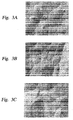
- Figure 1A shows a photomicrograph of the as-sintered surface of a solid yttrium oxide ceramic at a magnification of 1,000 times.
- Figure 1B shows a photomicrograph of the as-sintered surface of a solid solution ceramic substrate formed from 63 mole % yttrium oxide, 23 mole % zirconium oxide, and 14 mole % aluminum oxide, at a magnification of 1,000 times.
- Figure 1C shows a photomicrograph of the as-sintered surface of a solid solution ceramic substrate formed from 55 mole % yttrium oxide, 20 mole % zirconium oxide, and 25 mole % aluminum oxide, at a magnification of 1,000 times.
- Figure 2A shows a photomicrograph of the surface of a solid yttrium oxide ceramic after a test etch using the processing plasmas and times typically used to etch the various layers of a contact via feature in a semiconductor device.
- the magnification is 1,000 times.
- Figure 2B shows a photomicrograph of the surface of a solid solution ceramic formed from 63 mole % yttrium oxide, 23 mole % zirconium oxide, and 14 mole % aluminum oxide after a test etch using the processing plasmas and times typically used to etch the various layers of a contact via feature in a semiconductor device.
- the magnification is 1,000 times.
- Figure 2C shows a photomicrograph of the surface of a solid solution ceramic formed from 55 mole % yttrium oxide, 20 mole % zirconium oxide, and 25 mole % aluminum oxide after a test etch using the processing plasmas and times typically used to etch the various layers of a contact via feature in a semiconductor device.
- the magnification is 1,000 times.
- Figure 3A shows a photomicrograph of the post-etch ceramic of Figure 2A , but at a magnification of 5,000 times.
- Figure 3B shows a photomicrograph of the post-etch ceramic of Figure 2B , but at a magnification of 5,000 times.
- Figure 3C shows a photomicrograph of the post-etch ceramic of Figure 2C , but at a magnification of 5,000 times.
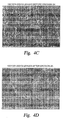
- Figure 4A shows a photomicrograph of the as-sintered surface of a solid solution ceramic formed from 63 mole % yttrium oxide, 23 mole % zirconium oxide, and 14 mole % aluminum oxide, at a magnification of 2,000 times.
- Figure 4B shows a photomicrograph of the surface of the solid solution ceramic shown in Figure 4A , after exposure of the test coupon to a trench etch process of the kind described herein.
- the magnification is 2,000 times.
- Figure 4C shows a photomicrograph of the as sintered surface of a solid solution ceramic formed from 55 mole % yttrium oxide, 20 mole % zirconium oxide, and 25 mole % aluminum oxide, at a magnification of 2,000 times.
- Figure 4D shows a photomicrograph of the surface of the solid solution ceramic shown in Figure 4C , after exposure of the test coupon to a trench etch process of the kind described herein.
- the magnification is 2,000 times.
- Figure 5A shows a photomicrograph of a solid solution ceramic formed from63 mole % yttrium oxide, 23 mole % zirconium oxide, and 14 mole % aluminum oxide after exposure of the test coupon to a metal etch process of the kind described herein.
- the magnification is 5,000 times.
- Figure 5B shows a photomicrograph of a solid solution ceramic formed from 55 mole % yttrium oxide, 20 mole % zirconium oxide, and 25 mole % aluminum oxide after exposure of the test coupon to an etch by a CF 4 /CHF 3 plasma. The magnification of 5,000 times.
- Bulk yttrium oxide has been shown to have very good corrosion resistance upon exposure to fluorine plasma and other corrosive plasmas which are typically used in semiconductor manufacturing processes (such as etch processes and chemical vapor deposition processes).
- pure crystalline yttrium oxide while offering very good corrosion resistance to various etchant plasmas, does not offer good mechanical properties in terms of flexural strength and fracture toughness, for example.
- Tables One - Three, below, provides the etch plasma compositions and etch plasma processing conditions which were used for evaluation of a series of test coupon materials.
- etch plasma conditions which were used for the erosion rate testing: 1) Trench etching, where the etch plasma source gas and etch process conditions were representative of etching a trench feature size beyond 65 nm technology, i.e. smaller than 65 nm, into a multilayered semiconductor substrate.
- Such a substrate typically includes an antireflective coating (ARC or BARC) layer, an organic or inorganic dielectric layer, a metal layer, and an etch stop layer.
- ARC or BARC antireflective coating
- etching where the etch plasma source gas and etch process conditions were representative of etching a contact via having an aspect ratio of about 30 in production and 40 plus in the developed device substrate, and having a diameter of beyond 65 nm technology into a multilayered semiconductor substrate including a buried ARC (BARC) layer, a dielectric layer and a stop layer; and 3) Metal etching, here the etch plasma source gas and etch process conditions were representative of etching an overlying titanium nitride hard mask and an aluminum layer, where the etch plasma source gas and etch process conditions are beyond 65 nm technology.
- BARC buried ARC
- the trench etching process and the contact via etching process were carried out in the ENABLER TM processing system, and the metal etching process was carried out in the DPS TM processing system, all available from Applied Materials, Inc. of Santa Clara, California.
- Example Two Comparative Relative Erosion Rates Of Various Ceramic Materials Compared With Aluminum Oxide
- Aluminum oxide has frequently been used as a protective layer or liner when a semiconductor process makes use of an etchant plasma.
- aluminum oxide as the base comparative material, we determined the relative etch rates, in a Trench Etch (CF 4 /CHF 3 ) environment. With aluminum oxide having a relative erosion rate of 1, we found that the relative erosion rate of quartz was about 2.2 times that of aluminum oxide.
- the relative erosion rate of silicon carbide was about 1.6 times that of aluminum oxide.
- the relative erosion rate of zirconia was about 0.8 times that of aluminum oxide.
- the relative erosion rate of pure yttrium oxide was about 0.19 times that of aluminum oxide.
- the relative erosion rate of a yttrium oxide, zirconium oxide, aluminum oxide ceramic composite, formed from 55 mole % yttrium oxide, 20 mole % zirconium oxide, and 25 mole % aluminum oxide was about 0.2 times that of aluminum oxide.
- the relative erosion rate of a yttrium oxide, zirconium oxide, aluminum oxide ceramic composite, formed from 63 mole % yttrium oxide, 23 mole % zirconium oxide, and 14 mole % aluminum oxide was about 0.05 times that of aluminum oxide.
- the sample substrate test coupon erosion rates measured were as follows.
- the erosion rate of aluminum oxide was 1.1 ⁇ m/hr.
- the erosion rate of bulk yttrium oxide was 0.3 ⁇ m/hr.
- the erosion rate of a the a yttrium oxide, zirconium oxide, aluminum oxide ceramic composite, formed from 55 mole % yttrium oxide, 20 mole % zirconium oxide, and 25 mole % aluminum oxide was 0.1 ⁇ m/hr.
- the erosion rate of a yttrium oxide, zirconium oxide, aluminum oxide ceramic composite, formed from 63 mole % yttrium oxide, 23 mole % zirconium oxide, and 14 mole % aluminum oxide was 0.07 ⁇ m/hr.
- the sample substrate test coupon erosion rates measured were as follows.
- the erosion rate of aluminum oxide was not measured.
- the erosion rate of bulk yttrium oxide was 0.16 ⁇ m/hr.
- the erosion rate of a the a yttrium oxide, zirconium oxide, aluminum oxide solid solution, formed from 55 mole % yttrium oxide, 20 mole % zirconium oxide, and 25 mole % aluminum oxide was 0.21 ⁇ m/hr.
- the erosion rate of a yttrium oxide, zirconium oxide, aluminum oxide solid solution, formed from 63 mole % yttrium oxide, 23 mole % zirconium oxide, and 14 mole % aluminum oxide was 0.22 ⁇ m/hr.
- the sample substrate test coupon erosion rates measured were as follows.
- the erosion rate of aluminum oxide was 4.10 ⁇ m/hr.
- the erosion rate for bulk yttrium oxide was 0.14 ⁇ m/hr.
- the erosion rate of a the a yttrium oxide, zirconium oxide, aluminum oxide ceramic composite, formed from 55 mole % yttrium oxide, 20 mole % zirconium oxide, and 25 mole % aluminum oxide was 0.10 ⁇ m/hr.
- the erosion rate of a yttrium oxide, zirconium oxide, aluminum oxide ceramic composite, formed from 63 mole % yttrium oxide, 23 mole % zirconium oxide, and 14 mole % aluminum oxide was 0.18 ⁇ m/hr.
- Figures 1A through 1C show photomicrographs of the surface of a sintered yttrium-oxide-containing ceramic composite prior to exposure to the via etch process described herein.
- the yttrium-oxide-containing ceramic composites include: 1) yttrium oxide-zirconium oxide solid solution; and 2) yttrium aluminate, when the composition was yttrium oxide 100 parts by weight, zirconium oxide 20 parts by weight, and aluminum oxide 10 parts by weight.
- This composition is the same as 63 mole % yttrium oxide, 23 mole % zirconium oxide, and 14 mole % aluminum oxide); and 3) yttrium oxide - zirconium oxide - aluminum oxide solid solution, when the composition from which the solid solution was formed was yttrium oxide 100 parts by weight, zirconium oxide 20 parts by weight, and aluminum oxide 20 parts by weight.
- This composition is the same as 55 mole % yttrium oxide, 20 mole % zirconium oxide, and 25 mole % aluminum oxide). All of the photomicrographs are at a magnification of 1,000 times.
- FIGS 2A through 2C show photomicrographs of the sintered yttrium-oxide-containing ceramic composite subsequent to exposure to the via etch process described herein.
- the yttrium-oxide-containing ceramic composites include: 1) yttrium oxide-zirconium oxide solid solution; and 2) yttrium aluminate, when the composition was yttrium oxide 100 parts by weight, zirconium oxide 20 parts by weight, and aluminum oxide 10 parts by weight (This composition is the same as 63 mole % yttrium oxide, 23 mole % zirconium oxide, and 14 mole % aluminum oxide); or when the composition was yttrium oxide 100 parts by weight, zirconium oxide 20 parts by weight, and aluminum oxide 20 parts by weight (This composition is the same as 55 mole % yttrium oxide, 20 mole % zirconium oxide, and 25 mole % aluminum oxide). All of the photomicrographs are at a magnification of 1,000 times.
- the surface roughness of the bulk yttrium oxide shown in Figure 2A has increased in roughness substantially. However, the overall surface roughness appears to be less than that of the zirconium oxide and aluminum oxide containing sample coupons.
- the surface roughness of the solid solution shown in Figure 2B which contains 10 parts by weight aluminum oxide appears to have hills and valleys which are flatter than the hills and valleys of the solid solution shown in Figure 2C , which contains the 20 parts by weight of aluminum oxide.
- the hills and valleys on the 10 parts by weight aluminum oxide sample coupon shown in Figure 2B have more pitting on the surface than in the 20 parts by weight sample coupon shown in Figure 2C .
- Figures 3A through 3C show photomicrographs which correspond with Figures 2A through 2C , respectively, but are at a magnification of 5,000 times. Looking at the surface of the bulk yttrium oxide sample coupon shown in Figure 3A , the surface is relatively smooth but does show some evidence of small pits.
- the Figure 3B solid solution formed from yttrium oxide 100 parts by weight, zirconium oxide 20 parts by weight, and aluminum oxide 10 parts by weight also shows some small scale pitting present on the rougher surface shown in Figure 2B .
- the Figure 3C solid solution formed from yttrium oxide 100 parts by weight, zirconium oxide 20 parts by weight, and aluminum oxide 20 parts by weigh shows negligible small scale pitting.
- the erosion rates were 0.16 ⁇ m/hr for the solid yttrium oxide shown in Figure 2A ; 0.22 ⁇ m/hr for the solid solution of yttrium oxide - zirconium oxide - aluminum oxide which contained 10 parts by weight aluminum oxide; and 0.21 ⁇ m/hr for the solid solution of yttrium oxide - zirconium oxide - aluminum oxide which contained 20 parts by weight aluminum oxide.
- Figure 4A shows a photomicrograph of the as-sintered surface of a solid solution ceramic composite containing 100 parts by weight yttrium oxide, 20 parts by weight aluminum oxide, and 10 parts by weight aluminum oxide (63 mole % yttrium oxide, 23 mole % zirconium oxide, and 14 mole % aluminum oxide), at a magnification of 2,000 times.
- Figure 4B shows a photomicrograph of the surface of the solid ceramic composite of Figure 4A after etching by a trench etch process of the kind shown herein. Both photomicrographs are at a magnification of 2,000.
- the post-etched surface appears to be flat and relatively homogeneous.
- Figure 4C shows a photomicrograph of the as-sintered surface of a solid solution ceramic composite containing 100 parts by weight yttrium oxide, 20 parts by weight aluminum oxide, and 20 parts by weight aluminum oxide (55 mole % yttrium oxide, 20 mole % zirconium oxide, and 25 mole % aluminum oxide).
- Figure 4D shows a photomicrograph of the surface of the solid solution ceramic composite of Figure 4C after etching by a trench etch process of the kind shown herein. Both photomicrographs are at a magnification of 2,000. The post-etched surface appears to be flat and relatively homogeneous. This combination of photographs suggests the same seasoning process described above for newly fabricated apparatus.
- the erosion rate of the solid solution ceramic composite containing the 20 parts by weight of aluminum oxide, after exposure to the trench etch process was about 0.07 ⁇ m/hr.
- Figure 5A shows a photomicrograph of a two phase solid solution ceramic composite formed from 100 parts by weight of yttrium oxide, 20 parts by weight of zirconium oxide and 10 parts by weight of aluminum oxide (63 mole % yttrium oxide, 23 mole % zirconium oxide, and 14 mole % aluminum oxide) after exposure of the test coupon to a metal etch process of the kind described herein.
- the magnification is 5,000 times.
- Figure 5B shows a photomicrograph of a two phase solid solution ceramic composite formed from 100 parts by weight of yttrium oxide, 20 parts by weight of zirconium oxide, and 10 parts by weight of aluminum oxide (55 mole % yttrium oxide, 20 mole % zirconium oxide, and 25 mole % aluminum oxide) after exposure of the test coupon to a metal etch process of the kind described herein.
- the magnification is 5,000 times.
- a comparison of these two photomicrographs shows that the two phase solid solution containing the higher content of aluminum oxide has an increased amount of the darker phase, which is yttrium aluminate.
- the erosion rate of the two phase solid solution ceramic composites containing the 10 parts by weight of aluminum oxide, after exposure to the trench etch process, was about 0.18 ⁇ m/hr, while the erosion rate of the two phase solid solution ceramic composite containing the 20 parts by weight of aluminum oxide, after exposure to the trench process was about 0.10 ⁇ m/hr.
- Table Four below shows comparative physical and mechanical properties for the bulk, pure yttrium oxide ceramic and for various yttrium-oxide containing solid solution ceramics.
- a starting composition for the ceramic materials may be one in which Y 2 O 3 molar concentration ranges from about 55 mole % to about 65 mole %, the ZrO 2 molar concentration ranges from about 10 mole % to about 25 mole % and the Al 2 O 3 molar concentration ranges from about 10 mole % to about 20 mole %.
- starting material concentration of the ceramic material may be one in which Y 2 O 3 molar concentration ranges from about 55 mole % to about 65 mole %, the ZrO 2 molar concentration ranges from about 20 mole % to about 25 mole % and the Al 2 O 3 molar concentration 5 mole % to about 10 mole %.
- Starting material compositions of the kind described above may be used to form a ceramic coating over the surface of a variety of metal or ceramic substrates, including but not limited to aluminum, aluminum alloy, stainless steel, alumina, aluminum nitride, and quartz, using a technique well known in the art, such as plasma spray, for example and not by way of limitation.
- plasma spray a technique well known in the art, such as plasma spray, for example and not by way of limitation.
- solid ceramic apparatus components be used when possible, to prevent sudden failure of plasma resistance due to coating layer flaking off, or defects in the coating which appear as the coating thins, or the formation of metal contamination by mobile impurities from the underlying substrate which migrate into the coating.
- the addition of a concentration of zirconium oxide ranging from about 0.1 mole % to about 65 mole % to what was a pure yttrium oxide, provides a solid solution of yttrium oxide and zirconium oxide with the cubic yttria crystal structure or cubic fluorite-type crystal structure, where the cell parameter is smaller than that of the pure structure, due to the formation of yttrium vacancy/oxygen vacancy, respectively.
- the smaller cell parameter of the solid solution crystal structure improves the plasma resistance properties of the solid solution of zirconium oxide in yttrium oxide.
- the erosion rate of a solid yttrium oxide ceramic in a CF 4 /CHF 3 plasma of the kind used to etch a trench in a multilayered semiconductor substrate is about 0.3 ⁇ m/hr.
- the erosion rate of a solid solution ceramic of about 69 mole % yttrium oxide and about 31 mole % zirconium oxide is about 0.1 ⁇ m/hr, a 3 times slower etch rate than solid yttrium oxide.
- This unexpected decrease in etch rate extends the lifetime of a process chamber liner or an internal apparatus component within the process chamber, so that: the replacement frequency for such apparatus is reduced, reducing apparatus down time; the particle amount generated during a process is reduced, improving the product properties; the metal contamination generated during a process is reduced, advancing the product properties; and the overall will reduce the overall cost of the processing apparatus per wafer processed will be reduced, on the average.
- the mechanical properties of the zirconium oxide-containing yttrium oxide solid solution illustrate that an improvement in flexural strength and fracture toughness would be helpful.
- the flexural strength and fracture toughness of the zirconium oxide-containing yttrium oxide solid solution are achieved, by adding various amounts of aluminum oxide to the formula for the solid solution ceramic to form an additional yttrium aluminate phase.
- the mixture of oxides was compacted by unidirectional mechanical pressing or cold isostatic pressing of a granular powder formed by spray drying, in combination with a typical content of binders.
- the green body was then pressureless sintered using techniques generally known in the art.
- the addition of 10 mole % to 30 mole % of alumina significantly improved the mechanical properties of the sintered ceramic composition in terms of flexural strength and fracture toughness.
- the erosion rate of the ceramic containing 69 mole % yttrium oxide and 31 mole % zirconium oxide, after exposure to a plasma containing CF 4 and CHF 3 was about 0.1 ⁇ m / hr.
- the erosion rate after exposure to the same plasma was also about 0.1 ⁇ m / hr.
- the erosion rate after exposure to the same plasma was about 0.2 ⁇ m / hr.
- an overall starting composition which is about 69 mole % yttrium oxide and about 31 mole % zirconium oxide, after sintering exhibits a flexural strength of about 137 Mpa, and a fracture toughness of 1.3 Mpa ⁇ m 1/2 , as discussed above.
- the overall ceramic composition is about 63 mole % yttrium oxide, about 23 mole % zirconium oxide, and about 14 mole % aluminum oxide, after sintering the flexural strength is about 215 Mpa and the fracture toughness is about 1.6 Mpa • m 1/2 .
- the overall ceramic composition is about 55 mole % yttrium oxide, about 20 mole % zirconium oxide, and about 25 mole % aluminum oxide, after sintering the flexural strength is about 172 Mpa and the fracture toughness is about 1.7 Mpa • m 1/2 .
- the relationship between aluminum oxide content, increase in flexural strength, and increase in erosion rate is not a linear relationship. However, one of skill in the art can optimize the formula with minimal experimentation, in view of the information provided herein.
- the concentration of the alternative compound in the starting material formulation ranges from about 0.1 mole % to about 90 mole %. Typically the concentration used will range from about 10 mole % to about 30 mole %.
- the combination of powders was compacted by unidirectionally mechanical pressing or cold isostatic pressing of the granular powder formed by spray drying with a typical content of binders.
- the green body was then pressureless sintered using techniques known in the art. Upon cooling of the sintered body, a single phase or two phase solid solution forms, where the solid solution is a "multi-element-doped" solid solution.
- One solid solution exhibits a cubic yttria crystal structure, and another solid solution exhibits the cubic fluorite-type crystal structure.
- the solid solution has excellent plasma resistance, typically better erosion resistance than that of the aluminum oxide-comprising solid solutions discussed herein.
- the mechanical properties of the yttria-zirconia-alumina system are somewhat better. All of these multi-doped solid solutions exhibit excellent plasma erosion resistance and improved mechanical properties in comparison with previously known yttrium oxide-zirconium oxide solid solutions.
- Typical applications for a yttrium oxide-comprising substrate of the kind described herein include, but are not limited to components used internal to a plasma processing chamber, such as a lid, lid-liner, nozzle, gas distribution plate or shower head, electrostatic chuck components, shadow frame, substrate holding frame, processing kit, and chamber liner. All of these components are well known in the art to those who do plasma processing.
- a ceramic article which is resistant to erosion by halogen-containing plasmas used in semiconductor processing said ceramic article including ceramic having at least two phases, said ceramic formed from yttrium oxide at a molar concentration ranging from about 50 mole % to about 75 mole %; zirconium oxide at a molar concentration ranging from about 10 mole % to about 30 mole %; and at least one other component selected from the group consisting of aluminum oxide, hafnium oxide, scandium oxide, neodymium oxide, niobium oxide, samarium oxide, ytterbium oxide, erbium oxide, cerium oxide, and combinations thereof, said at least one other component concentration ranging from about 10 mole % to about 30 mole %.
- a ceramic article in accordance with embodiment 1, wherein a flexural strength of said ceramic ranges from about 150 MPa to about 250 MPa.
- a ceramic article in accordance with embodiment 1, wherein a fracture toughness of said ceramic ranges from about 1.5 MPa ⁇ m 1/2 to about 2.0 MPa ⁇ m 1/2 .
- a method of reducing the plasma erosion of a semiconductor processing apparatus contacted by a halogen-containing plasma comprising: employing a ceramic-comprising article, said ceramic formed from yttrium oxide at a molar concentration ranging from about 50 mole % to about 75 mole %; zirconium oxide at a molar concentration ranging from about 10 mole % to about 30 mole %; and at least one other component selected from the group consisting of aluminum oxide, hafnium oxide, scandium oxide, neodymium oxide, niobium oxide, samarium oxide, ytterbium oxide, erbium oxide, cerium oxide, and combinations thereof, said at least one other component concentration ranging from about 10 mole % to about 30 mole %.
- said ceramic-comprising article is formed from yttrium oxide at a molar concentration ranging from about 55 mole % to about 65 mole %, zirconium oxide at a concentration ranging from about 15 mole % to about 25 mole % and said at least one other component at a concentration ranging from about 10 mole % to about 25 mole %.
- said ceramic-comprising article is formed from yttrium oxide at a concentration ranging from about 55 mole % to about 65 mole %, zirconium oxide at concentration ranging from about 20 mole % to about 25 mole %, and said at least one other component at a concentration ranging from about 10 mole % to about 20 mole %.
- a method in accordance with embodiment 14, wherein said plasma erosion rate for a surface of said semiconductor processing apparatus upon exposure to a halogen-comprising plasma ranges from about 0.1 ⁇ m/hr to about 0.3 ⁇ m/hr.
- a method in accordance with embodiment 16, wherein said plasma erosion rate for a surface of said semiconductor processing apparatus upon exposure to a halogen-comprising plasma ranges from about 0.1 ⁇ m/hr to about 0.3 ⁇ m/hr.
- a semiconductor processing apparatus which has at least one surface exposed to a halogen-comprising plasma during said semiconductor processing, wherein said semiconductor processing apparatus surface is a ceramic, said ceramic being resistant to erosion by halogen-containing plasmas, wherein said ceramic includes at least two phases and is formed from yttrium oxide at a molar concentration ranging from about 50 mole % to about 75 mole %; zirconium oxide at a molar concentration ranging from about 10 mole % to about 30 mole %; and at least one other component selected from the group consisting of aluminum oxide, hafnium oxide, scandium oxide, neodymium oxide, niobium oxide, samarium oxide, ytterbium oxide, erbium oxide, cerium oxide, and combinations thereof, said at least one other component concentration ranging from about 10 mole % to about 30 mole %.
- a ceramic article which is resistant to erosion by halogen-containing plasmas used in semiconductor processing comprising: a ceramic formed from a combination of yttrium oxide and zirconium oxide, with yttrium oxide at a molar concentration ranging from about 90 mole % to about 70 mole %, and zirconium oxide at a molar concentration ranging from about 10 mole % to about 30 mole %, wherein a mean grain size of said ceramic ranges from about 2 ⁇ m to about 8 ⁇ m.
- a ceramic article in accordance with embodiment 23, wherein a flexural strength of said ceramic ranges from about 120 MPa to about 140 MPa.
- a ceramic article in accordance with embodiment 23, wherein a fracture toughness of said ceramic ranges from about 1.1 MPa ⁇ m 1/2 to about 1.3 MPa ⁇ m 1/2 .
- a method of reducing the plasma erosion of a semiconductor processing apparatus contacted by a halogen-containing plasma comprising: selecting said semiconductor processing apparatus to comprise ceramic, said ceramic formed from yttrium oxide at a molar concentration ranging from about 90 mole % to about 70 mole %, and zirconium oxide at a molar concentration ranging from about 10 mole % to about 30 mole %.
- a method in accordance with embodiment 29 or 30, wherein said plasma erosion rate for a surface of said semiconductor processing apparatus upon exposure to a halogen-comprising plasma is less than about 0.2 ⁇ m/hr.
- a method in accordance with embodiment 31, wherein said plasma erosion rate for a surface of said semiconductor processing apparatus upon exposure to a halogen-comprising plasma ranges from about 0.1 ⁇ m/hr to about 0.2 ⁇ m/hr.
- a semiconductor processing apparatus having at least one surface exposed to a halogen-comprising plasma during a process, wherein said semiconductor processing apparatus surface is a ceramic which is resistant to erosion by halogen-containing plasmas, wherein said ceramic is formed from yttrium oxide at a molar concentration ranging from about 90 mole % to about 70 mole %, and zirconium oxide at a molar concentration ranging from about 10 mole % to about 30 mole %.
- a semiconductor processing apparatus said apparatus having at least one surface exposed to a halogen-comprising plasma during a process, wherein said surface is a ceramic which is resistant to erosion by halogen-containing plasmas, wherein said ceramic is formed from zirconium oxide at a molar concentration ranging from about 96 mole % to about 94 mole %, and yttrium oxide at a molar concentration ranging from about 4 mole % to about 6 mole %.
- a semiconductor processing apparatus in accordance with embodiment 36 wherein said apparatus is selected from the group consisting of a lid, a lid liner, a nozzle, a gas distribution plate, a shower head, an electrostatic chuck component, a shadow frame, a substrate holding frame, a processing kit, and a chamber liner.
- a semiconductor processing apparatus in accordance with embodiment 36, wherein a flexural strength of said ceramic ranges from about 1100 MPa to about 1300 MPa.
- a semiconductor processing apparatus in accordance with embodiment 36, wherein a fracture toughness of said ceramic ranges from about 10 MPa ⁇ m 1/2 to about 12 MPa ⁇ m 1/2 .
- a method of reducing the plasma erosion of a semiconductor processing apparatus contacted by a halogen-containing plasma comprising: selecting said semiconductor processing apparatus to be a ceramic-comprising article, said ceramic formed from zirconium oxide at a molar concentration ranging from about 96 mole % to about 94 mole %, and yttrium oxide at a molar concentration ranging from about 4 mole % to about 6 mole %.
Landscapes
- Chemical & Material Sciences (AREA)
- Engineering & Computer Science (AREA)
- Organic Chemistry (AREA)
- Plasma & Fusion (AREA)
- Analytical Chemistry (AREA)
- Physics & Mathematics (AREA)
- Ceramic Engineering (AREA)
- Materials Engineering (AREA)
- General Chemical & Material Sciences (AREA)
- Metallurgy (AREA)
- Mechanical Engineering (AREA)
- Manufacturing & Machinery (AREA)
- Chemical Kinetics & Catalysis (AREA)
- Structural Engineering (AREA)
- Composite Materials (AREA)
- Drying Of Semiconductors (AREA)
- Chemical Vapour Deposition (AREA)
- Physical Vapour Deposition (AREA)
- Inorganic Compounds Of Heavy Metals (AREA)
- Coating By Spraying Or Casting (AREA)
Applications Claiming Priority (2)
| Application Number | Priority Date | Filing Date | Title |
|---|---|---|---|
| US11/796,211 US7696117B2 (en) | 2007-04-27 | 2007-04-27 | Method and apparatus which reduce the erosion rate of surfaces exposed to halogen-containing plasmas |
| US11/796,210 US20080264564A1 (en) | 2007-04-27 | 2007-04-27 | Method of reducing the erosion rate of semiconductor processing apparatus exposed to halogen-containing plasmas |
Publications (2)
| Publication Number | Publication Date |
|---|---|
| EP1988187A2 true EP1988187A2 (fr) | 2008-11-05 |
| EP1988187A3 EP1988187A3 (fr) | 2010-12-08 |
Family
ID=39691093
Family Applications (1)
| Application Number | Title | Priority Date | Filing Date |
|---|---|---|---|
| EP08154940A Withdrawn EP1988187A3 (fr) | 2007-04-27 | 2008-04-22 | Appareil et procédé permettant de réduire le taux d'érosion des surfaces exposées aux plasmas contenant de l'halogène |
Country Status (6)
| Country | Link |
|---|---|
| EP (1) | EP1988187A3 (fr) |
| JP (7) | JP4975676B2 (fr) |
| KR (6) | KR100917292B1 (fr) |
| CN (1) | CN103102157A (fr) |
| SG (3) | SG142320A1 (fr) |
| TW (11) | TWI351057B (fr) |
Cited By (3)
| Publication number | Priority date | Publication date | Assignee | Title |
|---|---|---|---|---|
| US8871312B2 (en) | 2007-08-02 | 2014-10-28 | Applied Materials, Inc. | Method of reducing plasma arcing on surfaces of semiconductor processing apparatus components in a plasma processing chamber |
| US20180102237A1 (en) * | 2013-06-05 | 2018-04-12 | Applied Materials, Inc. | Rare-earth oxide based erosion resistant coatings for semiconductor application |
| WO2020206389A1 (fr) * | 2019-04-05 | 2020-10-08 | Heraeus Gmsi Llc | Oxyde d'yttrium à porosité contrôlée pour applications de gravure |
Families Citing this family (37)
| Publication number | Priority date | Publication date | Assignee | Title |
|---|---|---|---|---|
| TWI351057B (en) * | 2007-04-27 | 2011-10-21 | Applied Materials Inc | Method and apparatus which reduce the erosion rate of surfaces exposed to halogen-containing plasmas |
| US20100272982A1 (en) * | 2008-11-04 | 2010-10-28 | Graeme Dickinson | Thermal spray coatings for semiconductor applications |
| US9017765B2 (en) * | 2008-11-12 | 2015-04-28 | Applied Materials, Inc. | Protective coatings resistant to reactive plasma processing |
| JP2010174325A (ja) * | 2009-01-29 | 2010-08-12 | Kyocera Corp | 放電用電極体、放電用電極アセンブリおよび放電処理装置 |
| JP5526098B2 (ja) * | 2011-09-30 | 2014-06-18 | コバレントマテリアル株式会社 | 耐食性部材及びその製造方法 |
| JP2013079155A (ja) * | 2011-09-30 | 2013-05-02 | Covalent Materials Corp | 耐プラズマ性部材 |
| US9212099B2 (en) * | 2012-02-22 | 2015-12-15 | Applied Materials, Inc. | Heat treated ceramic substrate having ceramic coating and heat treatment for coated ceramics |
| US9343289B2 (en) * | 2012-07-27 | 2016-05-17 | Applied Materials, Inc. | Chemistry compatible coating material for advanced device on-wafer particle performance |
| US9711334B2 (en) * | 2013-07-19 | 2017-07-18 | Applied Materials, Inc. | Ion assisted deposition for rare-earth oxide based thin film coatings on process rings |
| US9583369B2 (en) * | 2013-07-20 | 2017-02-28 | Applied Materials, Inc. | Ion assisted deposition for rare-earth oxide based coatings on lids and nozzles |
| US9624593B2 (en) * | 2013-08-29 | 2017-04-18 | Applied Materials, Inc. | Anodization architecture for electro-plate adhesion |
| US9440886B2 (en) * | 2013-11-12 | 2016-09-13 | Applied Materials, Inc. | Rare-earth oxide based monolithic chamber material |
| CN104701125A (zh) * | 2013-12-05 | 2015-06-10 | 中微半导体设备(上海)有限公司 | 气体分布板 |
| US9725799B2 (en) | 2013-12-06 | 2017-08-08 | Applied Materials, Inc. | Ion beam sputtering with ion assisted deposition for coatings on chamber components |
| KR102437125B1 (ko) | 2014-06-27 | 2022-08-25 | 어플라이드 머티어리얼스, 인코포레이티드 | 고온 프로세싱을 위한 플라즈마 부식 저항성 가열기 |
| KR101465640B1 (ko) * | 2014-08-08 | 2014-11-28 | 주식회사 펨빅스 | 불화알루미늄 생성방지막이 형성된 cvd 공정챔버 부품 |
| US9850573B1 (en) * | 2016-06-23 | 2017-12-26 | Applied Materials, Inc. | Non-line of sight deposition of erbium based plasma resistant ceramic coating |
| KR101877017B1 (ko) * | 2017-01-09 | 2018-07-12 | 한국과학기술연구원 | 반도체 반응기 및 반도체 반응기용 금속모재의 코팅층 형성방법 |
| US10975469B2 (en) * | 2017-03-17 | 2021-04-13 | Applied Materials, Inc. | Plasma resistant coating of porous body by atomic layer deposition |
| US20180327892A1 (en) * | 2017-05-10 | 2018-11-15 | Applied Materials, Inc. | Metal oxy-flouride films for chamber components |
| US20190078199A1 (en) * | 2017-09-08 | 2019-03-14 | Applied Materials, Inc. | Rare-earth-based oxyfluoride ald coating for chamber productivity enhancement |
| US11014853B2 (en) * | 2018-03-07 | 2021-05-25 | Applied Materials, Inc. | Y2O3—ZrO2 erosion resistant material for chamber components in plasma environments |
| US11515128B2 (en) * | 2018-08-28 | 2022-11-29 | Lam Research Corporation | Confinement ring with extended life |
| US20220285164A1 (en) | 2019-07-22 | 2022-09-08 | Korea Institute Of Materials Science | Plasma Etching Apparatus Component for Manufacturing Semiconductor Comprising Composite Sintered Body and Manufacturing Method Therefor |
| KR102411792B1 (ko) | 2019-07-22 | 2022-06-22 | 한국재료연구원 | 복합 소결체를 포함하는 반도체 제조용 플라즈마 식각 장치 부품 및 그 제조방법 |
| WO2021020502A1 (fr) * | 2019-07-31 | 2021-02-04 | 京セラ株式会社 | Buse à gaz et dispositif de traitement au plasma l'utilisant |
| CN113053712B (zh) * | 2019-12-26 | 2023-12-01 | 中微半导体设备(上海)股份有限公司 | 一种等离子体处理装置及其气体喷嘴、气体喷嘴组件 |
| US20230150889A1 (en) * | 2020-04-27 | 2023-05-18 | Kyocera Corporation | Air-permeable member, member for semiconductor manufacturing device, plug, and adsorption member |
| US20230212082A1 (en) * | 2020-05-26 | 2023-07-06 | Heraeus Conamic North America Llc | Plasma resistant ceramic body formed from multiple pieces |
| CN114068276B (zh) * | 2020-08-05 | 2025-03-28 | 中微半导体设备(上海)股份有限公司 | 半导体零部件、等离子体反应装置和涂层形成方法 |
| CN114496690B (zh) * | 2020-10-27 | 2024-12-13 | 中微半导体设备(上海)股份有限公司 | 耐等离子体半导体零部件和形成方法、等离子体反应装置 |
| CN115142005A (zh) * | 2021-04-15 | 2022-10-04 | 浙江福腾宝家居用品有限公司 | 烹饪器具及其制备方法 |
| KR20240010724A (ko) * | 2021-07-07 | 2024-01-24 | 헤레우스 코나믹 노스 아메리카 엘엘씨 | 플라즈마 저항성 재료를 위한 이트리아-지르코니아 소결 세라믹 |
| KR102881899B1 (ko) * | 2021-12-10 | 2025-11-05 | 도카로 가부시키가이샤 | 플라즈마 에칭 장치용 부재 등에 적합한 성막 재료 및 그 제조 방법 |
| CN116332647A (zh) * | 2023-02-14 | 2023-06-27 | 沪硅精密陶瓷科技(苏州)有限公司 | 抗等离子体稀土氧化物固溶体陶瓷及其制造方法 |
| WO2025177799A1 (fr) * | 2024-02-21 | 2025-08-28 | Agc株式会社 | Film protecteur à base d'yttrium, élément et son procédé de production |
| WO2026014507A1 (fr) * | 2024-07-10 | 2026-01-15 | 住友大阪セメント株式会社 | Élément de mandrin électrostatique et dispositif de mandrin électrostatique |
Citations (8)
| Publication number | Priority date | Publication date | Assignee | Title |
|---|---|---|---|---|
| US5798016A (en) | 1994-03-08 | 1998-08-25 | International Business Machines Corporation | Apparatus for hot wall reactive ion etching using a dielectric or metallic liner with temperature control to achieve process stability |
| US20010003271A1 (en) | 1999-12-10 | 2001-06-14 | Tokyo Electron Limited | Processing apparatus with a chamber having therein a high-corrosion-resistant sprayed film |
| US6352611B1 (en) | 1998-07-29 | 2002-03-05 | Applied Materials, Inc. | Ceramic composition for an apparatus and method for processing a substrate |
| US6766873B2 (en) | 2001-08-23 | 2004-07-27 | General Motors Corporation | Fuel cell vehicle with by-wire technology |
| US6776873B1 (en) | 2002-02-14 | 2004-08-17 | Jennifer Y Sun | Yttrium oxide based surface coating for semiconductor IC processing vacuum chambers |
| US6777873B2 (en) | 2002-03-06 | 2004-08-17 | Pioneer Corporation | Plasma display panel |
| US20050037193A1 (en) | 2002-02-14 | 2005-02-17 | Sun Jennifer Y. | Clean, dense yttrium oxide coating protecting semiconductor processing apparatus |
| US20050056218A1 (en) | 2002-02-14 | 2005-03-17 | Applied Materials, Inc. | Gas distribution plate fabricated from a solid yttrium oxide-comprising substrate |
Family Cites Families (38)
| Publication number | Priority date | Publication date | Assignee | Title |
|---|---|---|---|---|
| US4360598A (en) * | 1980-03-26 | 1982-11-23 | Ngk Insulators, Ltd. | Zirconia ceramics and a method of producing the same |
| JPS63252963A (ja) * | 1987-04-07 | 1988-10-20 | イビデン株式会社 | ZrO↓2−La↓2O↓3−Y↓2O↓3系焼結体およびその製造方法 |
| JP2879255B2 (ja) * | 1990-09-21 | 1999-04-05 | 三徳金属工業株式会社 | 溶融酸化イットリウム成型体 |
| US5746875A (en) * | 1994-09-16 | 1998-05-05 | Applied Materials, Inc. | Gas injection slit nozzle for a plasma process reactor |
| ZA965340B (en) * | 1995-06-30 | 1997-01-27 | Interdigital Tech Corp | Code division multiple access (cdma) communication system |
| JPH09139219A (ja) * | 1995-11-15 | 1997-05-27 | Mitsubishi Heavy Ind Ltd | 固体電解質型電気化学セルおよびその製造方法 |
| JP2939535B2 (ja) * | 1997-03-28 | 1999-08-25 | 科学技術庁無機材質研究所長 | 透明酸化イットリウム焼結体の製造法 |
| JP2000001362A (ja) * | 1998-06-10 | 2000-01-07 | Nippon Seratekku:Kk | 耐食性セラミックス材料 |
| JP4544700B2 (ja) * | 1999-07-29 | 2010-09-15 | 京セラ株式会社 | 真空容器及びその製造方法 |
| JP3510993B2 (ja) * | 1999-12-10 | 2004-03-29 | トーカロ株式会社 | プラズマ処理容器内部材およびその製造方法 |
| JP4548887B2 (ja) * | 1999-12-27 | 2010-09-22 | 京セラ株式会社 | 耐食性セラミック部材およびその製造方法 |
| TW503449B (en) * | 2000-04-18 | 2002-09-21 | Ngk Insulators Ltd | Halogen gas plasma-resistive members and method for producing the same, laminates, and corrosion-resistant members |
| US6645585B2 (en) * | 2000-05-30 | 2003-11-11 | Kyocera Corporation | Container for treating with corrosive-gas and plasma and method for manufacturing the same |
| JP4688307B2 (ja) * | 2000-07-11 | 2011-05-25 | コバレントマテリアル株式会社 | 半導体製造装置用耐プラズマ性部材 |
| US6620520B2 (en) * | 2000-12-29 | 2003-09-16 | Lam Research Corporation | Zirconia toughened ceramic components and coatings in semiconductor processing equipment and method of manufacture thereof |
| JP2002255647A (ja) | 2001-02-27 | 2002-09-11 | Nihon Ceratec Co Ltd | 酸化イットリウム焼結体およびウエハ保持具 |
| TWI262905B (en) * | 2001-11-13 | 2006-10-01 | Tosoh Corp | Quartz glass parts, ceramic parts and process of producing those |
| JP2003146751A (ja) * | 2001-11-20 | 2003-05-21 | Toshiba Ceramics Co Ltd | 耐プラズマ性部材及びその製造方法 |
| JP4315363B2 (ja) * | 2001-12-03 | 2009-08-19 | 日本板硝子株式会社 | 薄膜形成方法 |
| US6942929B2 (en) * | 2002-01-08 | 2005-09-13 | Nianci Han | Process chamber having component with yttrium-aluminum coating |
| JP2003238250A (ja) * | 2002-02-12 | 2003-08-27 | Yotai Refractories Co Ltd | イットリア質耐火物 |
| US20080264564A1 (en) * | 2007-04-27 | 2008-10-30 | Applied Materials, Inc. | Method of reducing the erosion rate of semiconductor processing apparatus exposed to halogen-containing plasmas |
| JP2006507662A (ja) * | 2002-06-28 | 2006-03-02 | 東京エレクトロン株式会社 | プラズマ処理システム内のアーク抑制方法およびシステム |
| CN1412150A (zh) * | 2002-11-19 | 2003-04-23 | 中国科学院兰州化学物理研究所 | 自润滑陶瓷复合材料及制备工艺 |
| TW200423195A (en) * | 2002-11-28 | 2004-11-01 | Tokyo Electron Ltd | Internal member of a plasma processing vessel |
| JP2004268573A (ja) * | 2003-02-17 | 2004-09-30 | Toshiba Ceramics Co Ltd | Y2o3の鋳込み成型方法 |
| JP2004269951A (ja) * | 2003-03-07 | 2004-09-30 | Tocalo Co Ltd | 耐ハロゲンガス皮膜被覆部材およびその製造方法 |
| JP2005020641A (ja) * | 2003-06-30 | 2005-01-20 | Nec Engineering Ltd | 遠方監視制御装置 |
| US7141522B2 (en) * | 2003-09-18 | 2006-11-28 | 3M Innovative Properties Company | Ceramics comprising Al2O3, Y2O3, ZrO2 and/or HfO2, and Nb2O5 and/or Ta2O5 and methods of making the same |
| US7220497B2 (en) * | 2003-12-18 | 2007-05-22 | Lam Research Corporation | Yttria-coated ceramic components of semiconductor material processing apparatuses and methods of manufacturing the components |
| JP5046480B2 (ja) * | 2004-09-24 | 2012-10-10 | 京セラ株式会社 | 耐食性部材とその製造方法、およびこれを用いた半導体・液晶製造装置用部材 |
| CN1278989C (zh) * | 2005-05-25 | 2006-10-11 | 宜兴新兴锆业有限公司 | 一种改进的钇部分稳定二氧化锆生产方法 |
| US8617672B2 (en) * | 2005-07-13 | 2013-12-31 | Applied Materials, Inc. | Localized surface annealing of components for substrate processing chambers |
| US20070032072A1 (en) * | 2005-08-02 | 2007-02-08 | Stmicroelectronics Inc. | Nucleation layer deposition on semiconductor process equipment parts |
| KR100778274B1 (ko) * | 2005-08-16 | 2007-11-29 | 코바렌트 마테리얼 가부시키가이샤 | 산화 이트늄 소결체 및 그 제조 방법 |
| JP4936948B2 (ja) * | 2007-03-27 | 2012-05-23 | 日本碍子株式会社 | 複合材料及びその製造方法 |
| US10242888B2 (en) * | 2007-04-27 | 2019-03-26 | Applied Materials, Inc. | Semiconductor processing apparatus with a ceramic-comprising surface which exhibits fracture toughness and halogen plasma resistance |
| TWI351057B (en) * | 2007-04-27 | 2011-10-21 | Applied Materials Inc | Method and apparatus which reduce the erosion rate of surfaces exposed to halogen-containing plasmas |
-
2007
- 2007-07-04 TW TW096124359A patent/TWI351057B/zh active
- 2007-07-04 TW TW103132299A patent/TWI567793B/zh active
- 2007-07-04 TW TW107103413A patent/TWI654159B/zh active
- 2007-07-04 TW TW109115828A patent/TWI744898B/zh active
- 2007-07-04 TW TW107103418A patent/TWI654160B/zh active
- 2007-07-04 TW TW103132298A patent/TWI562205B/zh active
- 2007-07-04 TW TW100117999A patent/TWI483291B/zh active
- 2007-07-04 TW TW104122059A patent/TWI571452B/zh active
- 2007-07-04 TW TW108104769A patent/TWI695822B/zh active
- 2007-07-04 CN CN2012105926835A patent/CN103102157A/zh active Pending
- 2007-07-04 TW TW105136802A patent/TWI628154B/zh active
- 2007-07-04 TW TW107103401A patent/TWI654158B/zh active
- 2007-07-23 KR KR1020070073619A patent/KR100917292B1/ko active Active
-
2008
- 2008-04-07 JP JP2008099381A patent/JP4975676B2/ja active Active
- 2008-04-22 EP EP08154940A patent/EP1988187A3/fr not_active Withdrawn
- 2008-04-24 SG SG200803151-0A patent/SG142320A1/en unknown
- 2008-04-24 SG SG10201803162TA patent/SG10201803162TA/en unknown
- 2008-04-24 SG SG10201508616SA patent/SG10201508616SA/en unknown
-
2009
- 2009-02-26 KR KR1020090016418A patent/KR101365139B1/ko active Active
-
2012
- 2012-01-06 JP JP2012001609A patent/JP5805545B2/ja active Active
- 2012-12-20 KR KR1020120149865A patent/KR101428646B1/ko active Active
-
2013
- 2013-08-26 KR KR1020130101297A patent/KR101441865B1/ko active Active
-
2014
- 2014-01-24 KR KR20140008866A patent/KR101491568B1/ko active Active
- 2014-07-09 KR KR1020140086042A patent/KR101456539B1/ko active Active
-
2015
- 2015-05-28 JP JP2015108229A patent/JP6314110B2/ja active Active
-
2016
- 2016-01-15 JP JP2016006345A patent/JP6259844B2/ja active Active
- 2016-12-09 JP JP2016239304A patent/JP2017095350A/ja active Pending
-
2018
- 2018-11-20 JP JP2018217295A patent/JP2019069891A/ja active Pending
- 2018-11-21 JP JP2018218140A patent/JP2019069892A/ja active Pending
Patent Citations (10)
| Publication number | Priority date | Publication date | Assignee | Title |
|---|---|---|---|---|
| US5798016A (en) | 1994-03-08 | 1998-08-25 | International Business Machines Corporation | Apparatus for hot wall reactive ion etching using a dielectric or metallic liner with temperature control to achieve process stability |
| US6352611B1 (en) | 1998-07-29 | 2002-03-05 | Applied Materials, Inc. | Ceramic composition for an apparatus and method for processing a substrate |
| US20010003271A1 (en) | 1999-12-10 | 2001-06-14 | Tokyo Electron Limited | Processing apparatus with a chamber having therein a high-corrosion-resistant sprayed film |
| US6766873B2 (en) | 2001-08-23 | 2004-07-27 | General Motors Corporation | Fuel cell vehicle with by-wire technology |
| US6776873B1 (en) | 2002-02-14 | 2004-08-17 | Jennifer Y Sun | Yttrium oxide based surface coating for semiconductor IC processing vacuum chambers |
| US20050037193A1 (en) | 2002-02-14 | 2005-02-17 | Sun Jennifer Y. | Clean, dense yttrium oxide coating protecting semiconductor processing apparatus |
| US20050056218A1 (en) | 2002-02-14 | 2005-03-17 | Applied Materials, Inc. | Gas distribution plate fabricated from a solid yttrium oxide-comprising substrate |
| US20070134416A1 (en) | 2002-02-14 | 2007-06-14 | Applied Materials, Inc. | Cleaning method used in removing contaminants from the surface of an oxide or fluoride comprising a group III B metal |
| US20070151581A1 (en) | 2002-02-14 | 2007-07-05 | Applied Materials, Inc. | Cleaning method used in removing contaminants from a solid yttrium oxide-containing substrate |
| US6777873B2 (en) | 2002-03-06 | 2004-08-17 | Pioneer Corporation | Plasma display panel |
Cited By (4)
| Publication number | Priority date | Publication date | Assignee | Title |
|---|---|---|---|---|
| US8871312B2 (en) | 2007-08-02 | 2014-10-28 | Applied Materials, Inc. | Method of reducing plasma arcing on surfaces of semiconductor processing apparatus components in a plasma processing chamber |
| US20180102237A1 (en) * | 2013-06-05 | 2018-04-12 | Applied Materials, Inc. | Rare-earth oxide based erosion resistant coatings for semiconductor application |
| WO2020206389A1 (fr) * | 2019-04-05 | 2020-10-08 | Heraeus Gmsi Llc | Oxyde d'yttrium à porosité contrôlée pour applications de gravure |
| US12378163B2 (en) | 2019-04-05 | 2025-08-05 | Heraeus Covantics North America Llc | Controlled porosity yttrium oxide for etch applications |
Also Published As
Similar Documents
| Publication | Publication Date | Title |
|---|---|---|
| US11373882B2 (en) | Coated article and semiconductor chamber apparatus formed from yttrium oxide and zirconium oxide | |
| US7696117B2 (en) | Method and apparatus which reduce the erosion rate of surfaces exposed to halogen-containing plasmas | |
| US9051219B2 (en) | Semiconductor processing apparatus comprising a solid solution ceramic formed from yttrium oxide, zirconium oxide, and aluminum oxide | |
| EP1988187A2 (fr) | Appareil et procédé permettant de réduire le taux d'érosion des surfaces exposées aux plasmas contenant de l'halogène | |
| US10622194B2 (en) | Bulk sintered solid solution ceramic which exhibits fracture toughness and halogen plasma resistance |
Legal Events
| Date | Code | Title | Description |
|---|---|---|---|
| PUAI | Public reference made under article 153(3) epc to a published international application that has entered the european phase |
Free format text: ORIGINAL CODE: 0009012 |
|
| AK | Designated contracting states |
Kind code of ref document: A2 Designated state(s): AT BE BG CH CY CZ DE DK EE ES FI FR GB GR HR HU IE IS IT LI LT LU LV MC MT NL NO PL PT RO SE SI SK TR |
|
| AX | Request for extension of the european patent |
Extension state: AL BA MK RS |
|
| PUAL | Search report despatched |
Free format text: ORIGINAL CODE: 0009013 |
|
| AK | Designated contracting states |
Kind code of ref document: A3 Designated state(s): AT BE BG CH CY CZ DE DK EE ES FI FR GB GR HR HU IE IS IT LI LT LU LV MC MT NL NO PL PT RO SE SI SK TR |
|
| AX | Request for extension of the european patent |
Extension state: AL BA MK RS |
|
| RIC1 | Information provided on ipc code assigned before grant |
Ipc: C23C 4/10 20060101ALI20101029BHEP Ipc: H01J 37/32 20060101ALI20101029BHEP Ipc: C04B 41/87 20060101ALI20101029BHEP Ipc: C04B 35/505 20060101ALI20101029BHEP Ipc: C23C 16/44 20060101AFI20080825BHEP |
|
| STAA | Information on the status of an ep patent application or granted ep patent |
Free format text: STATUS: THE APPLICATION IS DEEMED TO BE WITHDRAWN |
|
| 18D | Application deemed to be withdrawn |
Effective date: 20101102 |