EP1988577A1 - Module DEL à plateforme de silicium - Google Patents
Module DEL à plateforme de silicium Download PDFInfo
- Publication number
- EP1988577A1 EP1988577A1 EP07117245A EP07117245A EP1988577A1 EP 1988577 A1 EP1988577 A1 EP 1988577A1 EP 07117245 A EP07117245 A EP 07117245A EP 07117245 A EP07117245 A EP 07117245A EP 1988577 A1 EP1988577 A1 EP 1988577A1
- Authority
- EP
- European Patent Office
- Prior art keywords
- led
- led module
- module according
- platform
- depression
- Prior art date
- Legal status (The legal status is an assumption and is not a legal conclusion. Google has not performed a legal analysis and makes no representation as to the accuracy of the status listed.)
- Granted
Links
Images

Classifications
-
- H—ELECTRICITY
- H10—SEMICONDUCTOR DEVICES; ELECTRIC SOLID-STATE DEVICES NOT OTHERWISE PROVIDED FOR
- H10W—GENERIC PACKAGES, INTERCONNECTIONS, CONNECTORS OR OTHER CONSTRUCTIONAL DETAILS OF DEVICES COVERED BY CLASS H10
- H10W90/00—Package configurations
-
- H—ELECTRICITY
- H10—SEMICONDUCTOR DEVICES; ELECTRIC SOLID-STATE DEVICES NOT OTHERWISE PROVIDED FOR
- H10H—INORGANIC LIGHT-EMITTING SEMICONDUCTOR DEVICES HAVING POTENTIAL BARRIERS
- H10H20/00—Individual inorganic light-emitting semiconductor devices having potential barriers, e.g. light-emitting diodes [LED]
- H10H20/80—Constructional details
- H10H20/85—Packages
- H10H20/855—Optical field-shaping means, e.g. lenses
- H10H20/856—Reflecting means
-
- H—ELECTRICITY
- H10—SEMICONDUCTOR DEVICES; ELECTRIC SOLID-STATE DEVICES NOT OTHERWISE PROVIDED FOR
- H10W—GENERIC PACKAGES, INTERCONNECTIONS, CONNECTORS OR OTHER CONSTRUCTIONAL DETAILS OF DEVICES COVERED BY CLASS H10
- H10W90/00—Package configurations
- H10W90/701—Package configurations characterised by the relative positions of pads or connectors relative to package parts
- H10W90/751—Package configurations characterised by the relative positions of pads or connectors relative to package parts of bond wires
- H10W90/754—Package configurations characterised by the relative positions of pads or connectors relative to package parts of bond wires between a chip and a stacked insulating package substrate, interposer or RDL
Definitions
- the present invention relates to a LED module having a silicon platform.
- US2005/2760553A discloses a LED package with a submount which may include one or more other electronic components for controlling the intensity of light emitted from the LED die.
- the "submount” is an insulating board which is inserted between the chip bottom and the package ground level. Besides the insulation, the submount has other roles of facilitating thermal diffusion, harmonizing the thermal expansion coefficients between the chip and the package or adjusting the height of the chip. In the case of enhancing thermal diffusion, regulating the thermal expansion coefficients or controlling the chip height, the submount need not be an insulator. In the case of the devices stored in metallic packages, the submount is a passive, intermediate chip base which plays the role of keeping a device chip upon a package. The submount usually has the dimensions of the base of the LED chip.
- the module comprises a platform with a depression formed in one side thereof. On a bottom surface of the depression there is arranged a LED chip.
- the platform may be made of a first silicon substrate and a second silicon substrate.
- the first silicon substrate forms a base part on top of which the second silicon substrate is arranged building a reflector.
- An integrated circuit may be arranged on the first substrate.
- a “platform” according to the present description is a component which at least laterally has greater dimensions than the LED chip.
- the LED chip can be mounted directly on the platform or indirectly, e.g. via a submount.
- the invention proposes a LED module having a LED semiconductor chip mounted directly or indirectly on a platform.
- the platform is made from silicon and extending laterally beyond the LED semiconductor chip having an active light emitting layer and a substrate, wherein in the silicon platform there is integrated at least one electronic component which is part of the control circuitry for the LED semiconductor chip.
- the integrated electronic component can be a sensor for the light intensity, the color temperature and/or the temperature.
- the integrated electronic component can be part of the LED drive electronics providing the LED semiconductor chip with power.
- the integrated electronic component can be a wireless communication device.
- the silicon platform can define a depression in which the LED semiconductor chip is arranged.
- the walls of the silicon platform defining the depression can vertically extend beyond the active light emitting layer of the LED semiconductor chip.
- the walls of the depression can be vertical, inclined or curved.
- the walls of the depression can be designed as reflector walls.
- the electronic component can be integrated in the walls of the silicon platform defining the depression.
- the electronic component can be integrated in the base part of the silicon platform.
- the depression can be at least partially filled with a color conversion medium.
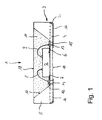
- Figure 1 shows a LED module 1 comprising a semiconductor LED chip 2.
- the LED chip 2 can be mounted in face-up or face-down geometry.
- the LED chip 2 has an active light emitting area and a substrate as it is well known from the prior art.
- the LED chip 2 is mounted directly on a silicon platform 3 or indirectly, i.e. by means of a submount which is not shown in the illustrated embodiment.
- the submount has lateral dimensions that correspond basically to the dimensions of the LED chip 2.
- the silicon platform 3 is not comparable with submounts.
- the shown silicon platform 3 extends laterally beyond the countours of the LED chip 2. It may also extend vertically beyond the LED chip 2 and particularly the active light emitting area of the LED chip 2.
- the silicon platform 3 may be designed to define an open cavity or depression 10, at the bottom 7 of which the LED chip 2 is arranged.
- the side walls of the depression 10 in the silicon platform 3 are constituted by the reflector and may be curved, vertical or inclined (as shown in the illustrated embodiment). They may serve as a reflector and can be metallised to this regard.
- the depression 10 may be filled at least partially with a color conversion layer 11 partially converting light emitted from the LED chip 2 into light having a different (longer) wavelength).
- the color conversion layer 11 may comprise phosphor embedded in a silicone mould.
- electronics is integrated in the silicon platform 3.
- This electronics may be or more of the following components:
- the electronics integrated in the platform 3 may be an integrated circuitry.
- platform 3 comprises a silicon substrate 4 which is a base part of platform 3.
- a first side of this silicon substrate 4 forms the bottom 7 of the depression 10 on which the LED chip 2 is mounted.
- the side walls are arranged protruding from the first side of the silicon substrate 4.
- the height of the walls is preferably greater than the height of the LED chip 2.
- the walls are made as a silicon reflector 5.
- the surface of the silicon reflector 5 which is directed to the depression 10 may be metallized in order to improve reflection.
- bonding wires 8, 9 are arranged and secured inside the silicon mould of the color conversion layer 11.
- the bonding wires 8, 9 connect the LED chip 2 with respective connecting areas 12, 13 which are arranged on the first side of silicon substrate 4 adjacent a mounting area 6 on which the LED chip 2 is mounted.
- the connecting areas 12, 13 are connected to a first electrode 16 and a second electrode 17 respectively by means of contact vias 14, 15.
- the first electrode 16 and the second electrode 17 are arranged on a second surface 18 of the silicon substrate 4 opposed to said first side 7 of the silicon substrate 4.
- the outer edges of the silicon substrate 4 are provided with a fillet area 20.
- electrodes 16, 17 follow the outer shape of the fillet area 20 of silicon substrate 4 thereby providing the LED module 1 with a contact area at the outer edge of the LED module 1.
- FIG 1 a basic structure of a LED module 1 according to the present invention is illustrated.
- the LED chip 2 can also be mounted on top of a submount which is consequently located between the LED chip 2 and the first surface 7 of the silicon substrate 4.
- the platform 3 comprising the silicon substrate 4 and the silicon reflector 5 may be fabricated by an edging process for example in order to generate depression 10 in which the LED chip 2 is arranged.
- the electronic component is preferably arranged in the walls of the silicon reflector 5 or in the silicon substrate 4. When the electronic component is arranged inside silicon substrate 4 it is arranged preferably nearer to the outer edge of the silicon substrate 4.
- the arrangement of the electronic component in the outer region of the platform 3 generally improves the sensing functionality. In particular if color temperature sensing is provided the sensing elements are not shaded by the LED chip itself or even by a submount.
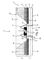
- the platform 3' is made of a number of individual layers that are laminated to build platform 3'.
- a first layer 31 and a second layer 32 build the base part of platform 3' together with a first intermediate layer 32.
- the first intermediate layer 33 is arranged on top of this first layer 31 and second layer 32.
- the base part of the platform 3' corresponds to the silicon substrate 4 of the first embodiment illustrated in fig. 1 .
- the first intermediate layer 33 comprises a central portion and an outer region 36. With the LED chip 2 being mounted on the central portion 35 of the first intermediate layer 33 it is preferred that the electronic component is arranged in the outer region 36 of the first intermediate layer 33.
- a second intermediate layer 34 is arranged on top of the first intermediate layer 33 .
- the second intermediate layer 34 is a first part of reflector 5'.
- an upper reflector part 36 is arranged on top of the second intermediate layer 34 arranged.
- the second intermediate layer 34 together with the upper reflector part 36 comprise an inclined surface defining depression 10 of the LED module 1.
- the arrangement of the electronic components in the platform 3 or 3' either in the silicon substrate or in the reflector has the advantage that different functions as light sensing or light colour sensing for example is improved.
- the sensing elements may be arranged besides the LED chip 2. Thereby light which is emitted by the LED chip 2 can be sensed by the electronic components in the silicon substrate 4 or the silicon reflector 5 without being shaded by the LED chip 2 or a submount. Although there is a direct contact to the depression area of the LED module 1 no additional space on the bottom surface of depression 10 is needed in order to arrange the electronic components adjacent to the LED chip 2.
- the further illustrated embodiment of a LED module 1" of figure 3 corresponds basically to that of figure 2 .
- the inner edges of the second intermediate layer 34' are provided with a rectangular edge.
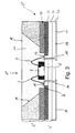
- FIG 4 there is shown a third embodiment. Contrary to figures 2 and 3 it is shown that the platform 3''' is made of three consecutive layers.
- a first layer forms the base part 40. Its shape defines the shape of depression 10.
- On top of the base part there is arranged a first additional layer 41 and a second additional layer 42.
- the shape of the first and the second additional layer 41, 42 correspond basically to the shape of the base part 40.
- the LED chip 2 is mounted on the second additional layer 42.
- the second additional layer 42 comprises a bottom surface 7' of the depression 10.
- the additional layers establish the reflector 50.
- the electronic component not under the LED chip 2 but adjacent to the LED chip 2. It is in particular preferred to locate the LED chip in a wall of the reflector.
- the reflector can be constituted from a number of consecutive layers.
- the electronic component comprises means for controlling the color temperature it is preferred to arrange the electronic component near the LED chip 2. Thereby it is preferred to arrange the electronic component inside either the first additional layer or the second additional layer.
- Platform 3 may comprise further layers.
- the invention is not limited to the illustrated embodiment but comprises also advantageous combinations of features of different embodiments.
Landscapes
- Led Device Packages (AREA)
Priority Applications (3)
| Application Number | Priority Date | Filing Date | Title |
|---|---|---|---|
| EP07117245.6A EP1988577B1 (fr) | 2007-04-30 | 2007-09-26 | Module à diode électroluminescente avec plateforme de silicium |
| PCT/EP2008/003387 WO2008131939A1 (fr) | 2007-04-30 | 2008-04-25 | Module de del à plate-forme de silicium |
| US12/527,240 US8569771B2 (en) | 2007-04-30 | 2008-04-25 | LED module with an LED semiconductor chip mounted on a silicon platform |
Applications Claiming Priority (2)
| Application Number | Priority Date | Filing Date | Title |
|---|---|---|---|
| EP07107236 | 2007-04-30 | ||
| EP07117245.6A EP1988577B1 (fr) | 2007-04-30 | 2007-09-26 | Module à diode électroluminescente avec plateforme de silicium |
Publications (2)
| Publication Number | Publication Date |
|---|---|
| EP1988577A1 true EP1988577A1 (fr) | 2008-11-05 |
| EP1988577B1 EP1988577B1 (fr) | 2017-04-05 |
Family
ID=39591416
Family Applications (1)
| Application Number | Title | Priority Date | Filing Date |
|---|---|---|---|
| EP07117245.6A Not-in-force EP1988577B1 (fr) | 2007-04-30 | 2007-09-26 | Module à diode électroluminescente avec plateforme de silicium |
Country Status (4)
| Country | Link |
|---|---|
| US (1) | US8569771B2 (fr) |
| EP (1) | EP1988577B1 (fr) |
| CN (1) | CN101663754A (fr) |
| WO (1) | WO2008131939A1 (fr) |
Cited By (4)
| Publication number | Priority date | Publication date | Assignee | Title |
|---|---|---|---|---|
| DE102009033915A1 (de) * | 2009-07-20 | 2011-01-27 | Osram Opto Semiconductors Gmbh | Verfahren zur Herstellung eines Leuchtmittels und Leuchtmittel |
| DE102010000738A1 (de) | 2009-11-25 | 2011-05-26 | Ledon Lighting Jennersdorf Gmbh | LED-Lampe mit Stiftsockel für Halogenlampen (Bipin) |
| US8273588B2 (en) | 2009-07-20 | 2012-09-25 | Osram Opto Semiconductros Gmbh | Method for producing a luminous device and luminous device |
| US9041295B2 (en) | 2009-04-09 | 2015-05-26 | Tridonic Jennersdorf Gmbh | Integrated LED and sensor device |
Families Citing this family (4)
| Publication number | Priority date | Publication date | Assignee | Title |
|---|---|---|---|---|
| TWI438889B (zh) * | 2010-12-01 | 2014-05-21 | 鴻海精密工業股份有限公司 | 發光二極體封裝結構 |
| JP5700544B2 (ja) * | 2011-04-14 | 2015-04-15 | 日東電工株式会社 | 発光ダイオード装置の製造方法 |
| TW201614345A (en) * | 2014-10-15 | 2016-04-16 | Taiwan Green Point Entpr Co | A method for manufacturing a light emitting assembly, the light emitting assembly and a backlight module comprising the light emitting assembly |
| DE102016219200A1 (de) | 2016-10-04 | 2018-04-05 | Tridonic Gmbh & Co Kg | Integrierte Anordnung modulierbarer Lichtpunkte für Kommunikation mittels sichtbarem Licht |
Citations (8)
| Publication number | Priority date | Publication date | Assignee | Title |
|---|---|---|---|---|
| US5003357A (en) * | 1987-05-30 | 1991-03-26 | Samsung Semiconductor And Telecommunications Co. | Semiconductor light emitting device |
| WO1999028971A1 (fr) * | 1997-05-15 | 1999-06-10 | Cis Institut Für Mikrosensorik | Composant electronique hybride et procede permettant de le produire |
| JPH11251644A (ja) * | 1998-02-27 | 1999-09-17 | Matsushita Electron Corp | 半導体発光装置 |
| JP2001015815A (ja) * | 1999-04-28 | 2001-01-19 | Sanken Electric Co Ltd | 半導体発光装置 |
| US20050127485A1 (en) * | 2003-12-11 | 2005-06-16 | Shih-Chang Shei | Light-emitting diode package structure |
| WO2005062393A2 (fr) * | 2003-12-09 | 2005-07-07 | Cree, Inc. | Dispositifs electroluminescents a semi-conducteurs, embases et procedes de production correspondants |
| EP1587151A2 (fr) * | 2004-04-17 | 2005-10-19 | Lg Electronics Inc. | Dispositif semi-conducteur d'émission de la lumière et méthode de fabrication |
| US20060071229A1 (en) * | 2004-10-01 | 2006-04-06 | Finisar Corporation | Integrated diode in a silicon chip scale package |
Family Cites Families (12)
| Publication number | Priority date | Publication date | Assignee | Title |
|---|---|---|---|---|
| US7344279B2 (en) | 2003-12-11 | 2008-03-18 | Philips Solid-State Lighting Solutions, Inc. | Thermal management methods and apparatus for lighting devices |
| KR100906475B1 (ko) * | 2004-01-13 | 2009-07-08 | 삼성전자주식회사 | 마이크로 광학벤치 구조물 및 그 제조방법 |
| US7165896B2 (en) * | 2004-02-12 | 2007-01-23 | Hymite A/S | Light transmitting modules with optical power monitoring |
| JP4572312B2 (ja) | 2004-02-23 | 2010-11-04 | スタンレー電気株式会社 | Led及びその製造方法 |
| WO2006011766A1 (fr) * | 2004-07-28 | 2006-02-02 | Epivalley Co., Ltd. | Dispositif optique dote d'un photodetecteur |
| DE112005001980T5 (de) * | 2004-08-18 | 2007-07-12 | National University Corporation Tokyo University Of Agriculture And Technology | Verfahren und Vorrichtung zur Gestaltmessung, sowie Frequenzkammlichtgenerator |
| KR100702569B1 (ko) * | 2005-09-12 | 2007-04-02 | 김광희 | 반사면 부착형 발광소자 |
| JP4757585B2 (ja) * | 2005-09-21 | 2011-08-24 | Nec液晶テクノロジー株式会社 | 光源ユニット及び照明装置 |
| US7766511B2 (en) * | 2006-04-24 | 2010-08-03 | Integrated Illumination Systems | LED light fixture |
| KR100854328B1 (ko) * | 2006-07-07 | 2008-08-28 | 엘지전자 주식회사 | 발광 소자 패키지 및 그 제조방법 |
| DE102006040641A1 (de) * | 2006-08-30 | 2008-03-13 | Robert Bosch Gmbh | Leuchtmodul |
| JP5127278B2 (ja) * | 2007-04-05 | 2013-01-23 | 三菱電機株式会社 | 熱型赤外線固体撮像素子及び赤外線カメラ |
-
2007
- 2007-09-26 EP EP07117245.6A patent/EP1988577B1/fr not_active Not-in-force
-
2008
- 2008-04-25 US US12/527,240 patent/US8569771B2/en not_active Expired - Fee Related
- 2008-04-25 WO PCT/EP2008/003387 patent/WO2008131939A1/fr not_active Ceased
- 2008-04-25 CN CN200880013170A patent/CN101663754A/zh active Pending
Patent Citations (8)
| Publication number | Priority date | Publication date | Assignee | Title |
|---|---|---|---|---|
| US5003357A (en) * | 1987-05-30 | 1991-03-26 | Samsung Semiconductor And Telecommunications Co. | Semiconductor light emitting device |
| WO1999028971A1 (fr) * | 1997-05-15 | 1999-06-10 | Cis Institut Für Mikrosensorik | Composant electronique hybride et procede permettant de le produire |
| JPH11251644A (ja) * | 1998-02-27 | 1999-09-17 | Matsushita Electron Corp | 半導体発光装置 |
| JP2001015815A (ja) * | 1999-04-28 | 2001-01-19 | Sanken Electric Co Ltd | 半導体発光装置 |
| WO2005062393A2 (fr) * | 2003-12-09 | 2005-07-07 | Cree, Inc. | Dispositifs electroluminescents a semi-conducteurs, embases et procedes de production correspondants |
| US20050127485A1 (en) * | 2003-12-11 | 2005-06-16 | Shih-Chang Shei | Light-emitting diode package structure |
| EP1587151A2 (fr) * | 2004-04-17 | 2005-10-19 | Lg Electronics Inc. | Dispositif semi-conducteur d'émission de la lumière et méthode de fabrication |
| US20060071229A1 (en) * | 2004-10-01 | 2006-04-06 | Finisar Corporation | Integrated diode in a silicon chip scale package |
Cited By (6)
| Publication number | Priority date | Publication date | Assignee | Title |
|---|---|---|---|---|
| US9041295B2 (en) | 2009-04-09 | 2015-05-26 | Tridonic Jennersdorf Gmbh | Integrated LED and sensor device |
| EP2417388B1 (fr) * | 2009-04-09 | 2016-02-10 | Tridonic Jennersdorf GmbH | Dispositif del et capteur intégré |
| DE102009033915A1 (de) * | 2009-07-20 | 2011-01-27 | Osram Opto Semiconductors Gmbh | Verfahren zur Herstellung eines Leuchtmittels und Leuchtmittel |
| US8273588B2 (en) | 2009-07-20 | 2012-09-25 | Osram Opto Semiconductros Gmbh | Method for producing a luminous device and luminous device |
| DE102010000738A1 (de) | 2009-11-25 | 2011-05-26 | Ledon Lighting Jennersdorf Gmbh | LED-Lampe mit Stiftsockel für Halogenlampen (Bipin) |
| WO2011064180A1 (fr) | 2009-11-25 | 2011-06-03 | Tridonic Jennersdorf Gmbh | Lampe à led munie d'un culot à broches pour lampes halogènes ('bipin') |
Also Published As
| Publication number | Publication date |
|---|---|
| US8569771B2 (en) | 2013-10-29 |
| CN101663754A (zh) | 2010-03-03 |
| US20110101381A1 (en) | 2011-05-05 |
| EP1988577B1 (fr) | 2017-04-05 |
| WO2008131939A1 (fr) | 2008-11-06 |
Similar Documents
| Publication | Publication Date | Title |
|---|---|---|
| US8569771B2 (en) | LED module with an LED semiconductor chip mounted on a silicon platform | |
| JP5226498B2 (ja) | 発光装置 | |
| EP2899762B1 (fr) | Emballage de dispositif électroluminescent | |
| EP2327582B1 (fr) | Boîtier de DEL, module de boîtier de DEL le comportant, module de phare doté de celui-ci et procédé de commande correspondant | |
| US6459130B1 (en) | Optoelectronic semiconductor component | |
| US8269244B2 (en) | LED package with efficient, isolated thermal path | |
| US20080296590A1 (en) | LED-Based Light Source Having Improved Thermal Dissipation | |
| JP5569389B2 (ja) | 発光装置の製造方法及び発光装置 | |
| US10559728B2 (en) | Semiconductor package structure | |
| US20120056227A1 (en) | Light emitting diode package and manufacturing method thereof | |
| TW201115792A (en) | Method for manufacturing an optoelectronic semiconductor component and said optoelectronic semiconductor component | |
| KR20110081306A (ko) | 반도체 소자를 위한 지지 몸체, 반도체 소자 및 지지 몸체의 제조 방법 | |
| US20160208987A1 (en) | Led module | |
| US20180182739A1 (en) | Light-emitting diode arrangement and method for the production thereof | |
| KR20130119908A (ko) | 발광 다이오드 | |
| JP2006303397A (ja) | 発光装置 | |
| KR100843734B1 (ko) | 반도체 전력용 모듈 및 그 제조방법 | |
| US20080006841A1 (en) | Light-emitting device | |
| JP2007324275A (ja) | 発光装置 | |
| JP2013183124A (ja) | 半導体発光装置 | |
| JP2007005722A (ja) | 光半導体素子用外囲器およびそれを用いた光半導体装置 | |
| CN113454796B (zh) | 光电子器件和用于制造光电子器件的方法 | |
| JP4967347B2 (ja) | 線状光源及び半導体発光ユニットの製法 | |
| JP7037044B2 (ja) | 発光装置及びその製造方法 | |
| KR20070058306A (ko) | 발광소자용 패키지 |
Legal Events
| Date | Code | Title | Description |
|---|---|---|---|
| PUAI | Public reference made under article 153(3) epc to a published international application that has entered the european phase |
Free format text: ORIGINAL CODE: 0009012 |
|
| AK | Designated contracting states |
Kind code of ref document: A1 Designated state(s): AT BE BG CH CY CZ DE DK EE ES FI FR GB GR HU IE IS IT LI LT LU LV MC MT NL PL PT RO SE SI SK TR |
|
| AX | Request for extension of the european patent |
Extension state: AL BA HR MK RS |
|
| 17P | Request for examination filed |
Effective date: 20090203 |
|
| 17Q | First examination report despatched |
Effective date: 20090306 |
|
| AKX | Designation fees paid |
Designated state(s): AT BE BG CH CY CZ DE DK EE ES FI FR GB GR HU IE IS IT LI LT LU LV MC MT NL PL PT RO SE SI SK TR |
|
| RAP1 | Party data changed (applicant data changed or rights of an application transferred) |
Owner name: TRIDONIC JENNERSDORF GMBH |
|
| GRAP | Despatch of communication of intention to grant a patent |
Free format text: ORIGINAL CODE: EPIDOSNIGR1 |
|
| STAA | Information on the status of an ep patent application or granted ep patent |
Free format text: STATUS: GRANT OF PATENT IS INTENDED |
|
| INTG | Intention to grant announced |
Effective date: 20161201 |
|
| GRAS | Grant fee paid |
Free format text: ORIGINAL CODE: EPIDOSNIGR3 |
|
| GRAA | (expected) grant |
Free format text: ORIGINAL CODE: 0009210 |
|
| STAA | Information on the status of an ep patent application or granted ep patent |
Free format text: STATUS: THE PATENT HAS BEEN GRANTED |
|
| AK | Designated contracting states |
Kind code of ref document: B1 Designated state(s): AT BE BG CH CY CZ DE DK EE ES FI FR GB GR HU IE IS IT LI LT LU LV MC MT NL PL PT RO SE SI SK TR |
|
| REG | Reference to a national code |
Ref country code: GB Ref legal event code: FG4D |
|
| REG | Reference to a national code |
Ref country code: CH Ref legal event code: EP |
|
| REG | Reference to a national code |
Ref country code: AT Ref legal event code: REF Ref document number: 882536 Country of ref document: AT Kind code of ref document: T Effective date: 20170415 |
|
| REG | Reference to a national code |
Ref country code: IE Ref legal event code: FG4D |
|
| REG | Reference to a national code |
Ref country code: DE Ref legal event code: R096 Ref document number: 602007050456 Country of ref document: DE |
|
| REG | Reference to a national code |
Ref country code: NL Ref legal event code: MP Effective date: 20170405 |
|
| REG | Reference to a national code |
Ref country code: LT Ref legal event code: MG4D |
|
| REG | Reference to a national code |
Ref country code: FR Ref legal event code: PLFP Year of fee payment: 11 |
|
| PG25 | Lapsed in a contracting state [announced via postgrant information from national office to epo] |
Ref country code: NL Free format text: LAPSE BECAUSE OF FAILURE TO SUBMIT A TRANSLATION OF THE DESCRIPTION OR TO PAY THE FEE WITHIN THE PRESCRIBED TIME-LIMIT Effective date: 20170405 |
|
| PG25 | Lapsed in a contracting state [announced via postgrant information from national office to epo] |
Ref country code: GR Free format text: LAPSE BECAUSE OF FAILURE TO SUBMIT A TRANSLATION OF THE DESCRIPTION OR TO PAY THE FEE WITHIN THE PRESCRIBED TIME-LIMIT Effective date: 20170706 Ref country code: LT Free format text: LAPSE BECAUSE OF FAILURE TO SUBMIT A TRANSLATION OF THE DESCRIPTION OR TO PAY THE FEE WITHIN THE PRESCRIBED TIME-LIMIT Effective date: 20170405 Ref country code: ES Free format text: LAPSE BECAUSE OF FAILURE TO SUBMIT A TRANSLATION OF THE DESCRIPTION OR TO PAY THE FEE WITHIN THE PRESCRIBED TIME-LIMIT Effective date: 20170405 Ref country code: FI Free format text: LAPSE BECAUSE OF FAILURE TO SUBMIT A TRANSLATION OF THE DESCRIPTION OR TO PAY THE FEE WITHIN THE PRESCRIBED TIME-LIMIT Effective date: 20170405 |
|
| PG25 | Lapsed in a contracting state [announced via postgrant information from national office to epo] |
Ref country code: BG Free format text: LAPSE BECAUSE OF FAILURE TO SUBMIT A TRANSLATION OF THE DESCRIPTION OR TO PAY THE FEE WITHIN THE PRESCRIBED TIME-LIMIT Effective date: 20170705 Ref country code: IS Free format text: LAPSE BECAUSE OF FAILURE TO SUBMIT A TRANSLATION OF THE DESCRIPTION OR TO PAY THE FEE WITHIN THE PRESCRIBED TIME-LIMIT Effective date: 20170805 Ref country code: SE Free format text: LAPSE BECAUSE OF FAILURE TO SUBMIT A TRANSLATION OF THE DESCRIPTION OR TO PAY THE FEE WITHIN THE PRESCRIBED TIME-LIMIT Effective date: 20170405 Ref country code: PL Free format text: LAPSE BECAUSE OF FAILURE TO SUBMIT A TRANSLATION OF THE DESCRIPTION OR TO PAY THE FEE WITHIN THE PRESCRIBED TIME-LIMIT Effective date: 20170405 Ref country code: LV Free format text: LAPSE BECAUSE OF FAILURE TO SUBMIT A TRANSLATION OF THE DESCRIPTION OR TO PAY THE FEE WITHIN THE PRESCRIBED TIME-LIMIT Effective date: 20170405 |
|
| PGFP | Annual fee paid to national office [announced via postgrant information from national office to epo] |
Ref country code: AT Payment date: 20170928 Year of fee payment: 11 |
|
| REG | Reference to a national code |
Ref country code: DE Ref legal event code: R097 Ref document number: 602007050456 Country of ref document: DE |
|
| PG25 | Lapsed in a contracting state [announced via postgrant information from national office to epo] |
Ref country code: RO Free format text: LAPSE BECAUSE OF FAILURE TO SUBMIT A TRANSLATION OF THE DESCRIPTION OR TO PAY THE FEE WITHIN THE PRESCRIBED TIME-LIMIT Effective date: 20170405 Ref country code: DK Free format text: LAPSE BECAUSE OF FAILURE TO SUBMIT A TRANSLATION OF THE DESCRIPTION OR TO PAY THE FEE WITHIN THE PRESCRIBED TIME-LIMIT Effective date: 20170405 Ref country code: SK Free format text: LAPSE BECAUSE OF FAILURE TO SUBMIT A TRANSLATION OF THE DESCRIPTION OR TO PAY THE FEE WITHIN THE PRESCRIBED TIME-LIMIT Effective date: 20170405 Ref country code: CZ Free format text: LAPSE BECAUSE OF FAILURE TO SUBMIT A TRANSLATION OF THE DESCRIPTION OR TO PAY THE FEE WITHIN THE PRESCRIBED TIME-LIMIT Effective date: 20170405 Ref country code: EE Free format text: LAPSE BECAUSE OF FAILURE TO SUBMIT A TRANSLATION OF THE DESCRIPTION OR TO PAY THE FEE WITHIN THE PRESCRIBED TIME-LIMIT Effective date: 20170405 |
|
| PLBE | No opposition filed within time limit |
Free format text: ORIGINAL CODE: 0009261 |
|
| STAA | Information on the status of an ep patent application or granted ep patent |
Free format text: STATUS: NO OPPOSITION FILED WITHIN TIME LIMIT |
|
| PG25 | Lapsed in a contracting state [announced via postgrant information from national office to epo] |
Ref country code: IT Free format text: LAPSE BECAUSE OF FAILURE TO SUBMIT A TRANSLATION OF THE DESCRIPTION OR TO PAY THE FEE WITHIN THE PRESCRIBED TIME-LIMIT Effective date: 20170405 |
|
| 26N | No opposition filed |
Effective date: 20180108 |
|
| REG | Reference to a national code |
Ref country code: CH Ref legal event code: PL |
|
| PG25 | Lapsed in a contracting state [announced via postgrant information from national office to epo] |
Ref country code: MC Free format text: LAPSE BECAUSE OF FAILURE TO SUBMIT A TRANSLATION OF THE DESCRIPTION OR TO PAY THE FEE WITHIN THE PRESCRIBED TIME-LIMIT Effective date: 20170405 Ref country code: SI Free format text: LAPSE BECAUSE OF FAILURE TO SUBMIT A TRANSLATION OF THE DESCRIPTION OR TO PAY THE FEE WITHIN THE PRESCRIBED TIME-LIMIT Effective date: 20170405 |
|
| REG | Reference to a national code |
Ref country code: IE Ref legal event code: MM4A |
|
| REG | Reference to a national code |
Ref country code: BE Ref legal event code: MM Effective date: 20170930 |
|
| PG25 | Lapsed in a contracting state [announced via postgrant information from national office to epo] |
Ref country code: LU Free format text: LAPSE BECAUSE OF NON-PAYMENT OF DUE FEES Effective date: 20170926 |
|
| REG | Reference to a national code |
Ref country code: DE Ref legal event code: R084 Ref document number: 602007050456 Country of ref document: DE |
|
| PG25 | Lapsed in a contracting state [announced via postgrant information from national office to epo] |
Ref country code: CH Free format text: LAPSE BECAUSE OF NON-PAYMENT OF DUE FEES Effective date: 20170930 Ref country code: LI Free format text: LAPSE BECAUSE OF NON-PAYMENT OF DUE FEES Effective date: 20170930 Ref country code: IE Free format text: LAPSE BECAUSE OF NON-PAYMENT OF DUE FEES Effective date: 20170926 |
|
| PG25 | Lapsed in a contracting state [announced via postgrant information from national office to epo] |
Ref country code: BE Free format text: LAPSE BECAUSE OF NON-PAYMENT OF DUE FEES Effective date: 20170930 |
|
| REG | Reference to a national code |
Ref country code: FR Ref legal event code: PLFP Year of fee payment: 12 |
|
| PG25 | Lapsed in a contracting state [announced via postgrant information from national office to epo] |
Ref country code: MT Free format text: LAPSE BECAUSE OF NON-PAYMENT OF DUE FEES Effective date: 20170926 |
|
| PGFP | Annual fee paid to national office [announced via postgrant information from national office to epo] |
Ref country code: FR Payment date: 20180927 Year of fee payment: 12 |
|
| PGFP | Annual fee paid to national office [announced via postgrant information from national office to epo] |
Ref country code: GB Payment date: 20180928 Year of fee payment: 12 |
|
| REG | Reference to a national code |
Ref country code: AT Ref legal event code: MM01 Ref document number: 882536 Country of ref document: AT Kind code of ref document: T Effective date: 20180926 |
|
| PG25 | Lapsed in a contracting state [announced via postgrant information from national office to epo] |
Ref country code: HU Free format text: LAPSE BECAUSE OF FAILURE TO SUBMIT A TRANSLATION OF THE DESCRIPTION OR TO PAY THE FEE WITHIN THE PRESCRIBED TIME-LIMIT; INVALID AB INITIO Effective date: 20070926 |
|
| PG25 | Lapsed in a contracting state [announced via postgrant information from national office to epo] |
Ref country code: AT Free format text: LAPSE BECAUSE OF NON-PAYMENT OF DUE FEES Effective date: 20180926 Ref country code: CY Free format text: LAPSE BECAUSE OF NON-PAYMENT OF DUE FEES Effective date: 20170405 |
|
| PG25 | Lapsed in a contracting state [announced via postgrant information from national office to epo] |
Ref country code: TR Free format text: LAPSE BECAUSE OF FAILURE TO SUBMIT A TRANSLATION OF THE DESCRIPTION OR TO PAY THE FEE WITHIN THE PRESCRIBED TIME-LIMIT Effective date: 20170405 |
|
| PG25 | Lapsed in a contracting state [announced via postgrant information from national office to epo] |
Ref country code: PT Free format text: LAPSE BECAUSE OF FAILURE TO SUBMIT A TRANSLATION OF THE DESCRIPTION OR TO PAY THE FEE WITHIN THE PRESCRIBED TIME-LIMIT Effective date: 20170405 |
|
| GBPC | Gb: european patent ceased through non-payment of renewal fee |
Effective date: 20190926 |
|
| PG25 | Lapsed in a contracting state [announced via postgrant information from national office to epo] |
Ref country code: FR Free format text: LAPSE BECAUSE OF NON-PAYMENT OF DUE FEES Effective date: 20190930 Ref country code: GB Free format text: LAPSE BECAUSE OF NON-PAYMENT OF DUE FEES Effective date: 20190926 |
|
| REG | Reference to a national code |
Ref country code: DE Ref legal event code: R081 Ref document number: 602007050456 Country of ref document: DE Owner name: TRIDONIC GMBH & CO KG, AT Free format text: FORMER OWNER: TRIDONIC JENNERSDORF GMBH, JENNERSDORF, AT |
|
| PGFP | Annual fee paid to national office [announced via postgrant information from national office to epo] |
Ref country code: DE Payment date: 20220927 Year of fee payment: 16 |
|
| P01 | Opt-out of the competence of the unified patent court (upc) registered |
Effective date: 20230530 |
|
| REG | Reference to a national code |
Ref country code: DE Ref legal event code: R119 Ref document number: 602007050456 Country of ref document: DE |
|
| PG25 | Lapsed in a contracting state [announced via postgrant information from national office to epo] |
Ref country code: DE Free format text: LAPSE BECAUSE OF NON-PAYMENT OF DUE FEES Effective date: 20240403 |