EP1989700B1 - Écran électronique à matrice active comprenant un circuit de commande à matrice de diodes - Google Patents
Écran électronique à matrice active comprenant un circuit de commande à matrice de diodes Download PDFInfo
- Publication number
- EP1989700B1 EP1989700B1 EP20060830939 EP06830939A EP1989700B1 EP 1989700 B1 EP1989700 B1 EP 1989700B1 EP 20060830939 EP20060830939 EP 20060830939 EP 06830939 A EP06830939 A EP 06830939A EP 1989700 B1 EP1989700 B1 EP 1989700B1
- Authority
- EP
- European Patent Office
- Prior art keywords
- pixel
- display
- driving circuit
- electrode
- row
- Prior art date
- Legal status (The legal status is an assumption and is not a legal conclusion. Google has not performed a legal analysis and makes no representation as to the accuracy of the status listed.)
- Not-in-force
Links
- 239000011159 matrix material Substances 0.000 title description 34
- 239000000758 substrate Substances 0.000 claims description 12
- 239000004065 semiconductor Substances 0.000 claims description 9
- 239000000463 material Substances 0.000 claims description 4
- 230000003287 optical effect Effects 0.000 description 10
- 238000000034 method Methods 0.000 description 5
- 230000008859 change Effects 0.000 description 4
- 239000010409 thin film Substances 0.000 description 4
- 230000008901 benefit Effects 0.000 description 3
- 238000004519 manufacturing process Methods 0.000 description 3
- 239000003990 capacitor Substances 0.000 description 2
- 239000002800 charge carrier Substances 0.000 description 2
- 239000004020 conductor Substances 0.000 description 2
- 238000005516 engineering process Methods 0.000 description 2
- 230000006870 function Effects 0.000 description 2
- 239000012212 insulator Substances 0.000 description 2
- 239000004973 liquid crystal related substance Substances 0.000 description 2
- 238000000059 patterning Methods 0.000 description 2
- 230000008569 process Effects 0.000 description 2
- 238000002310 reflectometry Methods 0.000 description 2
- 230000004044 response Effects 0.000 description 2
- 239000004983 Polymer Dispersed Liquid Crystal Substances 0.000 description 1
- 230000005540 biological transmission Effects 0.000 description 1
- 239000003086 colorant Substances 0.000 description 1
- 230000001419 dependent effect Effects 0.000 description 1
- 239000003989 dielectric material Substances 0.000 description 1
- 230000005684 electric field Effects 0.000 description 1
- AMGQUBHHOARCQH-UHFFFAOYSA-N indium;oxotin Chemical compound [In].[Sn]=O AMGQUBHHOARCQH-UHFFFAOYSA-N 0.000 description 1
- 238000010030 laminating Methods 0.000 description 1
- 238000003475 lamination Methods 0.000 description 1
- 230000014759 maintenance of location Effects 0.000 description 1
- 229910052751 metal Inorganic materials 0.000 description 1
- 239000002184 metal Substances 0.000 description 1
- 229910044991 metal oxide Inorganic materials 0.000 description 1
- 150000004706 metal oxides Chemical class 0.000 description 1
- 239000002245 particle Substances 0.000 description 1
- 230000010287 polarization Effects 0.000 description 1
- 230000009467 reduction Effects 0.000 description 1
- 238000010561 standard procedure Methods 0.000 description 1
Images




Classifications
-
- G—PHYSICS
- G02—OPTICS
- G02F—OPTICAL DEVICES OR ARRANGEMENTS FOR THE CONTROL OF LIGHT BY MODIFICATION OF THE OPTICAL PROPERTIES OF THE MEDIA OF THE ELEMENTS INVOLVED THEREIN; NON-LINEAR OPTICS; FREQUENCY-CHANGING OF LIGHT; OPTICAL LOGIC ELEMENTS; OPTICAL ANALOGUE/DIGITAL CONVERTERS
- G02F1/00—Devices or arrangements for the control of the intensity, colour, phase, polarisation or direction of light arriving from an independent light source, e.g. switching, gating or modulating; Non-linear optics
- G02F1/01—Devices or arrangements for the control of the intensity, colour, phase, polarisation or direction of light arriving from an independent light source, e.g. switching, gating or modulating; Non-linear optics for the control of the intensity, phase, polarisation or colour
- G02F1/13—Devices or arrangements for the control of the intensity, colour, phase, polarisation or direction of light arriving from an independent light source, e.g. switching, gating or modulating; Non-linear optics for the control of the intensity, phase, polarisation or colour based on liquid crystals, e.g. single liquid crystal display cells
- G02F1/133—Constructional arrangements; Operation of liquid crystal cells; Circuit arrangements
- G02F1/136—Liquid crystal cells structurally associated with a semi-conducting layer or substrate, e.g. cells forming part of an integrated circuit
- G02F1/1362—Active matrix addressed cells
- G02F1/1365—Active matrix addressed cells in which the switching element is a two-electrode device
-
- G—PHYSICS
- G02—OPTICS
- G02F—OPTICAL DEVICES OR ARRANGEMENTS FOR THE CONTROL OF LIGHT BY MODIFICATION OF THE OPTICAL PROPERTIES OF THE MEDIA OF THE ELEMENTS INVOLVED THEREIN; NON-LINEAR OPTICS; FREQUENCY-CHANGING OF LIGHT; OPTICAL LOGIC ELEMENTS; OPTICAL ANALOGUE/DIGITAL CONVERTERS
- G02F1/00—Devices or arrangements for the control of the intensity, colour, phase, polarisation or direction of light arriving from an independent light source, e.g. switching, gating or modulating; Non-linear optics
- G02F1/01—Devices or arrangements for the control of the intensity, colour, phase, polarisation or direction of light arriving from an independent light source, e.g. switching, gating or modulating; Non-linear optics for the control of the intensity, phase, polarisation or colour
- G02F1/165—Devices or arrangements for the control of the intensity, colour, phase, polarisation or direction of light arriving from an independent light source, e.g. switching, gating or modulating; Non-linear optics for the control of the intensity, phase, polarisation or colour based on translational movement of particles in a fluid under the influence of an applied field
- G02F1/166—Devices or arrangements for the control of the intensity, colour, phase, polarisation or direction of light arriving from an independent light source, e.g. switching, gating or modulating; Non-linear optics for the control of the intensity, phase, polarisation or colour based on translational movement of particles in a fluid under the influence of an applied field characterised by the electro-optical or magneto-optical effect
- G02F1/167—Devices or arrangements for the control of the intensity, colour, phase, polarisation or direction of light arriving from an independent light source, e.g. switching, gating or modulating; Non-linear optics for the control of the intensity, phase, polarisation or colour based on translational movement of particles in a fluid under the influence of an applied field characterised by the electro-optical or magneto-optical effect by electrophoresis
-
- G—PHYSICS
- G02—OPTICS
- G02F—OPTICAL DEVICES OR ARRANGEMENTS FOR THE CONTROL OF LIGHT BY MODIFICATION OF THE OPTICAL PROPERTIES OF THE MEDIA OF THE ELEMENTS INVOLVED THEREIN; NON-LINEAR OPTICS; FREQUENCY-CHANGING OF LIGHT; OPTICAL LOGIC ELEMENTS; OPTICAL ANALOGUE/DIGITAL CONVERTERS
- G02F2202/00—Materials and properties
- G02F2202/02—Materials and properties organic material
Definitions
- This invention relates to electronic displays and an improved switching control circuit based on diodes for the control of the circuit.
- a material in an electronic display, changes its optical state, e.g reflectivity, transmission or light emission, in response to an electrical signal such as a voltage or an injected current.
- LCDs liquid crystal displays
- the display architecture comprises a transparent front substrate coated with a transparent conductive electrode, e.g. Indium Tin Oxide (ITO), which may be patterned or unpatterned (the front plane), a back plane comprising electrodes which may optionally be transparent and an optional substrate which may also optionally be transparent, and the display medium place between the front and back plane.
- ITO Indium Tin Oxide
- the control of the optical state of the display results from the application of a voltage between the front and back plane electrodes which creates an electric field across the display medium or injects a current into the medium.
- the display may be divided into segments or, for more complicated information, into so-called pixels organised into a matrix of rows and columns.
- Such displays are commonly called bi-stable, even though many such displays are not strictly speaking truly bi-stable (having two stable states of equal energy), and this terminology will be applied herein as well.
- electrochromic displays such as reported and provided by NTera Inc. ( www.ntera.com )
- electrophoretic displays such as are reported and provided by E Ink Inc. (www.eink.com) and Sipix ( www.sipix.com ).
- E Ink Inc. www.eink.com
- Sipix www.sipix.com
- These displays show optical properties that in many ways are similar to ink on paper.
- these displays generally require an active matrix structure (an active electronic circuit controlling the electronic and optical state for each pixel) in order to display detailed information, as they are not addressable by passive matrix techniques and/or the response times are too slow for passive matrix line by line addressing.
- Active matrix circuits may be constructed on the basis of thin film transistors (TFTs), which are three terminal devices, or two terminal devices such as rectifying diodes and MIM diodes.
- TFTs have become the standard technique for LCDs.
- patterning is all done on the back plane of the display, with row and column lines connected to gate and source electrodes; the front plane electrode is typically unpatterned throughout the active area of the display.
- This has the advantage of reducing the requirements for alignment of front and back planes during assembly, which is especially important for displays which are made using printing technology and/or flexible substrates, e.g using organic semiconductors for the TFTs (see, for example, www.plasticlogic.com ).
- TFTs require very fine patterning steps and excellent semiconductor characteristics, especially charge carrier mobility, to perform adequately, and both issues become difficult when using printing technology and organic semiconductors.
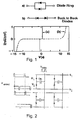
- diode-based active matrix back plane structures have been disclosed in the past and some have also been used commercially. Two structures are the diode ring and the back-to-back diode configuration, as seen in Fig. 1 .
- the display medium is in series with the diode circuit; the diode circuit and the display medium are placed between the row and column electrodes.
- FIG. 2 Another diode circuit design is called the two-diode switch, and the circuit is illustrated in Fig. 2 .
- This circuit configuration requires both a patterned front plane electrode structure and two select lines for each row of pixels.
- Patent application WO 2004/066410 discloses diode based circuits for active matrix back planes using single diode and back-to-back configurations, where the diodes are thin film diodes made using organic semiconductors ( Fig. 3 ).
- Two potential advantages of organic diodes over organic TFTs are less stringent requirements on charge carrier mobility and less stringent requirements on resolution due to the vertical instead of horizontal structure of the charge conducting layer. These two advantages can be especially significant for cost-efficient, high-throughput printing based manufacturing of active matrix back planes, as the resolution achievable with standard printing methods is limited.
- a patterned front plane electrode is used as in Fig. 1 and 2 .
- Metal-insulator-metal diode (M-I-M) diodes differ from rectifying diodes in that the current-voltage curves are symmetrical. MIM diodes have also been used to form active matrix back planes for displays; and example structure is shown in Fig. 4 . Note that also here the display medium (here a liquid crystal) is in series with the diode element in between row and column electrodes, i.e. the front plane electrode must be structured.
- Active matrix back planes based on solution processible MIM diodes have been disclosed in patent application disclosure WO 2004/051750 and in US patent 6,380,922 . In the former no description of a circuit or reduction to practice is given. In the latter, printed MIM diodes based on inorganic metal oxides are claimed for use in active matrix displays, preferably electrophoretic displays. An unpatterned front plane electrode is used in the proposed circuit, which can drive a single pixel, but no disclosure is made how an entire matrix of rows and columns could effectively be driven.
- US patent 6,980,196 discloses an electronic display where the display medium is particle based, e.g. electrophoretic, and controlled by an active matrix which may comprise printable nonlinear diode elements, the intention being the fabrication of a printable active matrix display.
- the display medium is placed in series with the nonlinear device between row and column electrodes, i.e. the disclosure requires patterned front plane electrodes.
- having structured elements on both the front and back plane create additional alignment difficulty, especially if printing and lamination processes are used for display fabrication and assembly.
- some display media e.g. electrophoretic and polymer-dispersed liquid crystal media, are frequently commercially available primarily as front plane laminates with the active display medium already laminated onto an unpatterned front plane.
- an object of the invention is to disclose a diode based back plane circuit that can drive a display medium, especially a bistable display medium, effectively in a matrix configuration such that row and column address lines are both on the back plane and the front plane is essentially unpatterned in the active display area. Furthermore, the driving circuit matrix should be able to drive a full matrix display with good contrast between optical states, and with the highest possible power efficiency.
- the invention discloses diode based backplane circuits that are able to drive a display medium, especially a bi-stable display medium, in an active matrix mode with a minimum of additional voltage and leakage current, without the need for a patterned front plane, and with optical performance comparable to directly driven displays and TFT active matrix displays
- the diode active matrix back plane disclosed herein comprises a matrix of row and column address lines on the back plane, with two rectifying diodes in series between the row and column lines, plus a load impedance in series with the diodes and disposed between the second diode and the row line.
- the display medium is located between the backplane and an unstructured front plane electrode structure, and the back pixel electrode of the display medium is connected to the diode circuit between the two diodes.
- the back plane architecture and the addressing scheme used are suitable for bi-stable display media possessing a short circuit memory (i.e. able to maintain an image even when the front and back electrodes are connected and at the same potential) without a patterned front plane. All the pixel capacitors share a common front electrode
- the display pixel electrode is still connected to the circuit between the two diodes, but the load resistor is made unnecessary, by choosing a diode - diode configuration in which the diodes have different forward resistances at chosen current values.
- the pixel electrode is connected to the circuit between a source lead at either a driving voltage or ground and two diodes which are connected to the row and column lines.
- this circuit functions like an AND or OR gate to drive the pixels.
- This circuit is also able to drive a bistable display with an unpatterned front plane.
- a driving circuit for a bistable display as defined by claim 1.
- a unit cell of which is shown in Fig. 5 the unit cell 10 (pixel) of the diode active matrix back plane disclosed herein comprises a connection to row address lines 11 and column address lines 12 on the back plane, with two rectifying diodes 13 and 14 in series between the row and column lines, plus a load impedance 15 in series with the diodes and disposed between the second diode and the row line.
- the display medium is located between the backplane and an unstructured front plane electrode structure, and the pixel back electrode 16 of the display medium is connected to the diode circuit between the two diodes.
- Fig. 6 The relationship of impedances in a single pixel element is sketched in Fig. 6 .
- the resistance RI of the load resistor 15 is dominant wherein the forward bias resistance Rf of the diodes 13, 14 is negligible and the voltage drop is essentially over this load resistor 15.
- the resistances Rr of the diodes 13, 14 are dominant wherein the resistance RI of the load resistor 15 is negligible.
- the following truth table describes the state of the pixel back electrode as a function of the voltages on the row 11 and column address line 12 to which it is connected via the circuit according to the invention. If the voltage in the row address line 11 (row voltage) is at 0 that row is selected and the state of the pixel can be changed. A voltage of 0 at the column address line 12 (column voltage) will cause a charged pixel to discharge at a time defined by the load resistance and the pixel capacitance, while an uncharged pixel remains uncharged. A column voltage of Vs will not change the state of a pixel electrode at Vs-Vd but will charge an uncharged pixel to Vs.
- the loading impedance In addition to enabling the control of the pixel state, the loading impedance also enables to lower the current consumption of the diode active matrix backplane. This is due to the current limiting nature of the loading impedance.
- the load impedance is at least 100 kOhm and especially preferred if the load impedance is over 1 MOhm.
- the value of the loading impedance must be selected such that Rf ⁇ RI ⁇ Rr, where Rf is the forward impedance of the diodes, RI the load impedance of the pixel and Rr is the reverse impedance of the diodes.
- the reverse bias current of the diodes is advantageously less than 1 ⁇ A per pixel, preferentially less than 1 nA.
- the rectification ratio of the diodes is advantageously larger than 100, and preferentially larger than 1000.
- the load resistor is replaced by a diode - diode configuration in which the diodes have different forward resistances at chosen current values. This can be taken into account with the driving wave forms by setting the pixel capacitors to the same voltage as the front plane.
- the driving scheme is realised with diode logic gated with either AND or OR structure.
- a unit circuit for the AND configuration is shown in Fig. 7 and the truth table is analysed similarly to the embodiment above.
- the unit cell 20 of the diode active matrix back plane comprises a connection to row and column address lines 21 and 22 and a source voltage Vs 23 on the back plane. Between the source and the row and column electrodes are disposed diodes 24 and 25 and load resistor 26. The back pixel electrode 27 is disposed between the load resistor and the diodes. In the AND configuration the pixel electrode is discharged to 0 unless both the row and column are at Vs.
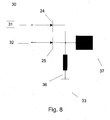
- a unit circuit for the OR configuration is shown in Fig. 8 and the truth table is analysed similarly to the embodiment above.
- the unit cell 30 of the diode active matrix back plane comprises a connection to row and column address lines 31 and 32 and to a ground connetion 33 on the back plane. Between the ground and the row and column electrodes are disposed diodes 24 and 25 and load resistor 26. The back pixel electrode 37 is disposed between the load resistor and the diodes. In the OR configuration the pixel electrode is at Vs if either the row is column are at Vs and 0 if both are at 0.
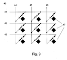
- a matrix backplane 40 can be constructed by connecting row electrodes and column electrodes together as described in figure 9 for the first embodiment described. Row electrodes 41-43 and column electrodes 44 - 46 are disposed on the back plane of a display, with unit circuits 47 disposed between the row and column electrodes as disclosed above.
- the embodiments described above can drive a display under assumption that the display medium is bistable and has a short circuit memory, i.e. the medium does not change its optical state if there is no potential difference between the front and back plane electrodes.
- a display driving scheme according to the invention is based on the fact that if there is no potential difference between the pixel electrode and the front plane the pixel remains optically unchanged. This enables possibility to construct a circuit and driving scheme in such a way that once a row is unselected all pixel electrodes in that row are in the same potential with front plane.
- the following example illustrates a driving scheme for a bistable display according to Fig. 9 .
- the front plane potential is initially set to Vs-Vd. Setting a row to Vs results in a situation where all the pixels at that row will be set to Vs-Vd. As this is the same potential as the front plane the optical state of the pixel will remain unchanged. However if the row is selected by setting it to 0, which is a different potential compared to the front plane, it is possible to determine the pixel voltage by controlling the state of the column electrodes. If a column is set to Vs the pixel is unchanged, since the voltage in pixel electrode is Vs-Vd. If the column voltage is set to 0 the pixel voltage decays to 0 at a fairly rapid rate determined by the load resistance and generates a potential difference between the pixel electrode and front plane. Therefore the optical state of the pixel is changed as there is a potential difference between front plane and pixel electrode.
- the pixel driving is reset at the end of each row driving sequence. This is done by setting all pixel electrodes to the same potential as front plane. This is done by setting the front plane to Vs-Vd, the row to be reset to Vs and all column electrodes to Vs.
- the diodes comprise organic semiconductor material, especially solution processed organic semiconductor material. It is especially preferred if the diodes and if possible also the resistors are deposited by printing techniques, especially for organic semiconductor diodes.
- the display medium is a bi-stable display medium, especially a reflective display medium, and in particular an electrophoretic display medium. It is especially preferred if the back plane, the front plane and the display medium are all flexible.
- a display is manufactured by preparing a back plane structure according to the circuits described above, with the same advantageous embodiments as described for the circuit and the display, then laminating a display medium previously laminated onto an unpatterned front plane electrode structure to the back plane to make an active matrix display.
- An active matrix backplane 50 comprises row lines 51-53, insulators 54 disposed on top of the row lines, column lines 55-57 crossing the row lines at the points where the insulators are deposited, and between the row and column lines diodes 58, resistors 59 and pixel electrodes 60 laterally oriented and connected in such as way as to form unit cells as shown in Fig. 5 .
- WO 2004//070466 discloses a version of a vertical pixel architecture, useful for e.g. electrophoretic displays, on the basis of thin film transistors (TFTs), whereby the pixel electrode is disposed above the TFT matrix, separated by a dielectric material layer, and connected to the drain electrode by means of a via hole in the dielectric.
- TFTs thin film transistors
- US patent 6,232,950 discloses a display architecture in which conductors are disposed onto a substrate, covered by a dielectric layer with via holes, and a pixel electrode is deposited onto the dielectric layer in such a way that the via holes are filled and electrical connection is made to the lead lines.
- a matrix based on thin film diodes and resistors i.e. a structure comprising not only conductive patterns but also active components comprising semiconductors may also be disposed underneath the pixel electrode.
- Fig. 11 demonstrates one embodiment of such a display architecture according to the invention in the example of a single pixel 100.
- a substrate 101 Upon a substrate 101 are disposed a row line 102, resistor 103, diodes 104 and 105, column line 110 and a dielectric layer comprising vias 109.
- a pixel electrode 106 Upon this is disposed a pixel electrode 106 in such a way that the vias are filled and make contact between the pixel electrode and the driving circuit.
- the display electrode 106 is adjacent to the display medium 107 and the front plane electrode 108.
- US patent 6,445,374 discloses a display architecture in which conductors are disposed onto one side of a substrate comprising via holes at appropriate locations, the pixel electrodes are disposed onto the other side of the substrate and contact is made through filling of the via holes.
- a vertical pixel architecture for circuits according to the invention as sketched in Fig. 12 in the example of a single pixel 200.
- a substrate 201 comprising vias 209 are disposed on one side of the substrate a row line 202, resistor 203, diodes 204 and 205 and column line 210.
- a pixel electrode 206 On the other side of the substrate 201 is disposed a pixel electrode 206 in such a way that the vias are filled and make contact between the pixel electrode and the driving circuit.
- the display electrode 206 is adjacent to the display medium 207 and the front plane electrode 208.
- Fig. 13 illustrates an example of a device 130 in which the driving system of the present invention can be implemented.
- the device 130 is, for example, an electronic price label, an information display, etc.
- the device 130 comprises a controller 131 for controlling the operation of the device 130.
- the device 130 also comprises a memory 132 for storing information, software programs, parameters etc.
- the device may also have an input element 133 for inputting information such as price data, updated versions of software, new parameter values, etc.
- the device 130 may also comprise a keyboard 134 which the user can use to input data to the device 130.
- the display driver 136 of the device 130 forms the row and column voltages for each row address lines and column address lines so that pixels of the display 137 are in a desired state to show information to be displayed. Also when the information to be dissplayed changes the display driver 136 makes the necessary adjustments to the row and column voltages. It is noted here that the row and column voltages are dependent on inter alia which of the embodiments disclosed herein is used.
- Information to be shown may be stored into the memory 132.
- the memory may contain also a look-up table in which the current state of each pixel is stored, since the driving waveform needed to switch the pixel to another state or maintain the current state depends on the current state of the pixel.
- the controller 130 reads the information from the memory 132 e.g. pixel by pixel and sends the information to the display driver 136.
- the display driver 136 sets correct row and column voltages on the row and column address lines as was disclosed above in connection with Fig. 9 . Changes to row and column voltages are only necessary when one or more pixel states need to be changed thus power consumption can be kept very low.
- the driving circuit of the invention is also applicable to colour display.
- each pixel element is divided into a plurality of sub-pixels, e.g. red, green and blue or cyan, yellow and magenta, each created for example by use of an appropriate colour filter with a black and white display medium or use of patterned display media with different colours.
- a white sub-pixel may also be added to a reflective display to increase the display brightness.
- Each sub-pixel will then be controlled by its own pixel control circuit as disclosed herein.
Landscapes
- Physics & Mathematics (AREA)
- Nonlinear Science (AREA)
- Engineering & Computer Science (AREA)
- Microelectronics & Electronic Packaging (AREA)
- Mathematical Physics (AREA)
- Chemical & Material Sciences (AREA)
- Crystallography & Structural Chemistry (AREA)
- General Physics & Mathematics (AREA)
- Optics & Photonics (AREA)
- Control Of Indicators Other Than Cathode Ray Tubes (AREA)
- Devices For Indicating Variable Information By Combining Individual Elements (AREA)
- Liquid Crystal (AREA)
Claims (13)
- Circuit de pilotage pour un afficheur bistable, le circuit de pilotage comprenant- une première borne agencée de façon à être connectée à une électrode de rangée (11) de l'afficheur bistable ;- une deuxième borne agencée de façon à être connectée à une électrode de colonne (12) de l'afficheur bistable ;- une troisième borne agencée de façon à être connectée à une électrode de pixel (16, 27, 37) de l'afficheur bistable ;- une impédance de charge ;- une première diode de redressement (13, 24) connectée entre la deuxième borne et la troisième borne ;- une deuxième diode de redressement (14, 25) connectée en série avec l'impédance de charge entre la première borne et la troisième borne, dans lequel ladite première diode de redressement (13, 24) est connectée directement de la deuxième borne à la troisième borne, ladite deuxième diode de redressement (14, 25) est connectée directement de la troisième borne à l'impédance de charge, et ladite impédance de charge est connectée à la première borne, et- ladite au moins une électrode de rangée (11), ladite au moins une électrode de colonne (12) et ladite électrode de pixel sont sur le même côté de l'afficheur bistable.
- Circuit de pilotage selon la revendication 1, dans lequel ladite impédance de charge comprend une résistance de charge.
- Circuit de pilotage selon la revendication 1, dans lequel ladite impédance de charge est intégrée dans une des diodes de redressement.
- Circuit de pilotage selon la revendication 2, dans lequel le circuit de pilotage est formé sur une plaque arrière de l'afficheur bistable, le circuit de pilotage comprenant en outre un substrat (101), dans lequel l'électrode de rangée (11), l'électrode de colonne (12), l'impédance de charge (15), la première diode de redressement (13, 24), et la deuxième diode de redressement (14, 25) sont sur le substrat, et le circuit de pilotage comprenant en outre une couche diélectrique ayant un trou de raccordement (109) pour connecter l'électrode de pixel au circuit de pilotage.
- Circuit de pilotage selon l'une quelconque des revendications 1 à 3, dans lequel ladite première diode de redressement (13, 24) est connectée directement de l'électrode de rangée à l'électrode de pixel, et ladite deuxième diode de redressement (14, 25) est connectée directement de l'électrode de colonne à l'électrode de pixel.
- Circuit de pilotage selon l'une quelconque des revendications 1 à 3, dans lequel ladite première diode de redressement (13, 24) est connectée directement de l'électrode de pixel à l'électrode de rangée, et ladite deuxième diode de redressement (14, 25) est connectée directement de l'électrode de pixel à l'électrode de colonne.
- Circuit de pilotage selon l'une quelconque des revendications 1 à 6, dans lequel l'appareil est configuré pour utiliser un courant de polarisation inverse des diodes de redressement qui est inférieur à 1 µA par pixel.
- Afficheur selon l'une quelconque des revendications 1 à 7, dans lequel l'appareil est configuré pour utiliser un courant de polarisation inverse des diodes de redressement qui est inférieur à 1 nA par pixel.
- Circuit de pilotage selon l'une quelconque des revendications 1 à 8, dans lequel au moins une diode de redressement comprend un matériau semiconducteur organique.
- Afficheur comprenant- une pluralité d'électrodes de rangée (11) ;- une pluralité d'électrodes de colonne (12) ;- une pluralité de pixels (10, 20, 30), chaque pixel de ladite pluralité de pixels étant attribué à un croisement d'une électrode de rangée (11) et d'une électrode de colonne (12) ;- une pluralité d'électrodes de pixel (16, 27, 37) attribuée chacune à un pixel ;- un support d'afficheur bistable ;dans lequel ladite au moins une électrode de rangée (11), ladite au moins une électrode de colonne (12) et ladite électrode de pixel sont sur le même côté du support d'afficheur bistable et l'afficheur comprend en outre une pluralité de circuits de pilotage selon l'une quelconque des revendications 1 à 9.
- Afficheur selon la revendication 10, dans lequel la valeur de l'impédance de charge RI est telle que Rf<RI<Rr, où Rf est l'impédance directe de la première diode de redressement et de la deuxième diode de redressement, RI est l'impédance de charge du pixel et Rr est l'impédance inverse de la première diode de redressement et de la deuxième diode de redressement.
- Dispositif (130) comprenant le circuit de pilotage selon l'une quelconque des revendications 1 à 9.
- Dispositif (130) comprenant l'afficheur selon la revendication 10.
Applications Claiming Priority (2)
| Application Number | Priority Date | Filing Date | Title |
|---|---|---|---|
| US77679506P | 2006-02-27 | 2006-02-27 | |
| PCT/FI2006/050566 WO2007096456A1 (fr) | 2006-02-27 | 2006-12-19 | Ecran electronique a matrice active comprenant un circuit d'entrainement de matrice a base de diode |
Publications (3)
| Publication Number | Publication Date |
|---|---|
| EP1989700A1 EP1989700A1 (fr) | 2008-11-12 |
| EP1989700A4 EP1989700A4 (fr) | 2009-08-26 |
| EP1989700B1 true EP1989700B1 (fr) | 2015-05-20 |
Family
ID=38436977
Family Applications (1)
| Application Number | Title | Priority Date | Filing Date |
|---|---|---|---|
| EP20060830939 Not-in-force EP1989700B1 (fr) | 2006-02-27 | 2006-12-19 | Écran électronique à matrice active comprenant un circuit de commande à matrice de diodes |
Country Status (3)
| Country | Link |
|---|---|
| US (1) | US8395611B2 (fr) |
| EP (1) | EP1989700B1 (fr) |
| WO (1) | WO2007096456A1 (fr) |
Families Citing this family (3)
| Publication number | Priority date | Publication date | Assignee | Title |
|---|---|---|---|---|
| US9060146B2 (en) * | 2009-01-06 | 2015-06-16 | Next Biometrics Group Asa | Low noise reading architecture for active sensor arrays |
| IT1399180B1 (it) * | 2009-06-12 | 2013-04-11 | Sharp Kk | Simulatore solare |
| US10446585B2 (en) * | 2014-03-17 | 2019-10-15 | E Ink Corporation | Multi-layer expanding electrode structures for backplane assemblies |
Family Cites Families (16)
| Publication number | Priority date | Publication date | Assignee | Title |
|---|---|---|---|---|
| US4666252A (en) * | 1984-06-29 | 1987-05-19 | Energy Conversion Devices, Inc. | High yield liquid crystal display and method of making same |
| US4728172A (en) * | 1984-08-08 | 1988-03-01 | Energy Conversion Devices, Inc. | Subassemblies for displays having pixels with two portions and capacitors |
| US6067062A (en) * | 1990-09-05 | 2000-05-23 | Seiko Instruments Inc. | Light valve device |
| DE69212690T2 (de) * | 1991-04-24 | 1997-02-27 | Philips Electronics Nv | Anzeigevorrichtung |
| US6980196B1 (en) | 1997-03-18 | 2005-12-27 | Massachusetts Institute Of Technology | Printable electronic display |
| US6232950B1 (en) * | 1997-08-28 | 2001-05-15 | E Ink Corporation | Rear electrode structures for displays |
| US6380922B1 (en) * | 1999-04-16 | 2002-04-30 | The Gillette Company | Electronic display |
| WO2001082382A1 (fr) * | 2000-04-20 | 2001-11-01 | Digirad Corporation | Fabrication de photodiodes illuminées sur l'envers à courant de fuite faible |
| KR100534573B1 (ko) * | 2000-11-29 | 2005-12-07 | 삼성에스디아이 주식회사 | 트라이오드 정류 스위치 |
| KR100388272B1 (ko) * | 2000-12-26 | 2003-06-19 | 삼성에스디아이 주식회사 | 티알에스 소자 |
| TW550528B (en) * | 2002-03-29 | 2003-09-01 | Chi Mei Optoelectronics Corp | Display device |
| AU2003298135A1 (en) * | 2002-11-29 | 2004-06-23 | Siemens Aktiengesellschaft | Diode matrix for controlling displays with organic diodes and production method therefor |
| EP1584114A1 (fr) | 2003-01-17 | 2005-10-12 | Diode Solutions, Inc. | Afficheur utilisant une matiere organique |
| GB0302485D0 (en) | 2003-02-04 | 2003-03-05 | Plastic Logic Ltd | Pixel capacitors |
| US7580033B2 (en) * | 2003-07-16 | 2009-08-25 | Honeywood Technologies, Llc | Spatial-based power savings |
| KR100666548B1 (ko) * | 2003-11-26 | 2007-01-09 | 삼성에스디아이 주식회사 | 트라이오드 정류스위치를 포함하는 표시장치 |
-
2006
- 2006-12-19 EP EP20060830939 patent/EP1989700B1/fr not_active Not-in-force
- 2006-12-19 WO PCT/FI2006/050566 patent/WO2007096456A1/fr not_active Ceased
- 2006-12-19 US US12/280,949 patent/US8395611B2/en not_active Expired - Fee Related
Also Published As
| Publication number | Publication date |
|---|---|
| US20090085904A1 (en) | 2009-04-02 |
| US8395611B2 (en) | 2013-03-12 |
| WO2007096456A1 (fr) | 2007-08-30 |
| EP1989700A4 (fr) | 2009-08-26 |
| EP1989700A1 (fr) | 2008-11-12 |
Similar Documents
| Publication | Publication Date | Title |
|---|---|---|
| US8586989B2 (en) | Thin film transistor array panel and display device | |
| US20190064256A1 (en) | Test circuit, array substrate and manufacturing method thereof, and display device | |
| CN101114431B (zh) | 液晶显示器 | |
| US20030206331A1 (en) | Matrix driven electrophoretic display with multilayer back plane | |
| JP2005512124A (ja) | 積層型透過性エレクトロルミネセント表示素子を備えたディスプレイ装置 | |
| KR20070004460A (ko) | 전기 광학 배치 구조 | |
| KR20080097330A (ko) | 전자 잉크 디스플레이 패널 | |
| CN101655646A (zh) | 显示装置及其制造方法 | |
| US20090195492A1 (en) | Liquid crystal display device | |
| KR101754799B1 (ko) | 화소 회로, 이를 포함하는 디스플레이 장치 및 디스플레이 장치의 구동방법 | |
| KR100993420B1 (ko) | 액정표시장치 | |
| US20090295710A1 (en) | Electrophoretic display device and electronic apparatus | |
| CN105047143A (zh) | 显示面板及其驱动方法、显示装置 | |
| KR102647463B1 (ko) | 전기 광학 디스플레이들 | |
| KR100924222B1 (ko) | 정전기 방전 회로 및 이를 구비한 액정표시장치 | |
| KR20050035500A (ko) | 박막 트랜지스터, 박막 트랜지스터 표시판 및 표시 장치 | |
| US5596342A (en) | Display device having separate short circuit wires for data and gate lines for protection against static discharges | |
| JP5409352B2 (ja) | 移動粒子表示装置 | |
| EP1989700B1 (fr) | Écran électronique à matrice active comprenant un circuit de commande à matrice de diodes | |
| US20080111787A1 (en) | Electrophoretic display device and method of driving the same | |
| KR101263659B1 (ko) | 전기영동 표시 장치 및 그 제조방법 | |
| KR101233145B1 (ko) | 액정표시장치 | |
| US7433006B2 (en) | Liquid crystal display with low consumption storage capacitors | |
| US20190072831A1 (en) | Substrate and display panel | |
| JP5478395B2 (ja) | 電気泳動表示装置及びその駆動方法 |
Legal Events
| Date | Code | Title | Description |
|---|---|---|---|
| PUAI | Public reference made under article 153(3) epc to a published international application that has entered the european phase |
Free format text: ORIGINAL CODE: 0009012 |
|
| 17P | Request for examination filed |
Effective date: 20080828 |
|
| AK | Designated contracting states |
Kind code of ref document: A1 Designated state(s): AT BE BG CH CY CZ DE DK EE ES FI FR GB GR HU IE IS IT LI LT LU LV MC NL PL PT RO SE SI SK TR |
|
| A4 | Supplementary search report drawn up and despatched |
Effective date: 20090724 |
|
| 17Q | First examination report despatched |
Effective date: 20090929 |
|
| DAX | Request for extension of the european patent (deleted) | ||
| RAP1 | Party data changed (applicant data changed or rights of an application transferred) |
Owner name: SMARTRAC IP B.V. |
|
| REG | Reference to a national code |
Ref country code: DE Ref legal event code: R079 Ref document number: 602006045495 Country of ref document: DE Free format text: PREVIOUS MAIN CLASS: G09G0003360000 Ipc: G02F0001136500 |
|
| GRAP | Despatch of communication of intention to grant a patent |
Free format text: ORIGINAL CODE: EPIDOSNIGR1 |
|
| INTG | Intention to grant announced |
Effective date: 20141121 |
|
| RIC1 | Information provided on ipc code assigned before grant |
Ipc: G02F 1/1365 20060101AFI20141112BHEP Ipc: G02F 1/167 20060101ALI20141112BHEP |
|
| GRAS | Grant fee paid |
Free format text: ORIGINAL CODE: EPIDOSNIGR3 |
|
| GRAA | (expected) grant |
Free format text: ORIGINAL CODE: 0009210 |
|
| AK | Designated contracting states |
Kind code of ref document: B1 Designated state(s): AT BE BG CH CY CZ DE DK EE ES FI FR GB GR HU IE IS IT LI LT LU LV MC NL PL PT RO SE SI SK TR |
|
| REG | Reference to a national code |
Ref country code: GB Ref legal event code: FG4D |
|
| REG | Reference to a national code |
Ref country code: CH Ref legal event code: EP |
|
| REG | Reference to a national code |
Ref country code: AT Ref legal event code: REF Ref document number: 728009 Country of ref document: AT Kind code of ref document: T Effective date: 20150615 |
|
| REG | Reference to a national code |
Ref country code: IE Ref legal event code: FG4D |
|
| REG | Reference to a national code |
Ref country code: DE Ref legal event code: R096 Ref document number: 602006045495 Country of ref document: DE Effective date: 20150702 |
|
| REG | Reference to a national code |
Ref country code: AT Ref legal event code: MK05 Ref document number: 728009 Country of ref document: AT Kind code of ref document: T Effective date: 20150520 |
|
| REG | Reference to a national code |
Ref country code: LT Ref legal event code: MG4D |
|
| REG | Reference to a national code |
Ref country code: NL Ref legal event code: MP Effective date: 20150520 |
|
| PG25 | Lapsed in a contracting state [announced via postgrant information from national office to epo] |
Ref country code: PT Free format text: LAPSE BECAUSE OF FAILURE TO SUBMIT A TRANSLATION OF THE DESCRIPTION OR TO PAY THE FEE WITHIN THE PRESCRIBED TIME-LIMIT Effective date: 20150921 Ref country code: ES Free format text: LAPSE BECAUSE OF FAILURE TO SUBMIT A TRANSLATION OF THE DESCRIPTION OR TO PAY THE FEE WITHIN THE PRESCRIBED TIME-LIMIT Effective date: 20150520 Ref country code: LT Free format text: LAPSE BECAUSE OF FAILURE TO SUBMIT A TRANSLATION OF THE DESCRIPTION OR TO PAY THE FEE WITHIN THE PRESCRIBED TIME-LIMIT Effective date: 20150520 Ref country code: FI Free format text: LAPSE BECAUSE OF FAILURE TO SUBMIT A TRANSLATION OF THE DESCRIPTION OR TO PAY THE FEE WITHIN THE PRESCRIBED TIME-LIMIT Effective date: 20150520 |
|
| PG25 | Lapsed in a contracting state [announced via postgrant information from national office to epo] |
Ref country code: AT Free format text: LAPSE BECAUSE OF FAILURE TO SUBMIT A TRANSLATION OF THE DESCRIPTION OR TO PAY THE FEE WITHIN THE PRESCRIBED TIME-LIMIT Effective date: 20150520 Ref country code: GR Free format text: LAPSE BECAUSE OF FAILURE TO SUBMIT A TRANSLATION OF THE DESCRIPTION OR TO PAY THE FEE WITHIN THE PRESCRIBED TIME-LIMIT Effective date: 20150821 Ref country code: BG Free format text: LAPSE BECAUSE OF FAILURE TO SUBMIT A TRANSLATION OF THE DESCRIPTION OR TO PAY THE FEE WITHIN THE PRESCRIBED TIME-LIMIT Effective date: 20150820 Ref country code: IS Free format text: LAPSE BECAUSE OF FAILURE TO SUBMIT A TRANSLATION OF THE DESCRIPTION OR TO PAY THE FEE WITHIN THE PRESCRIBED TIME-LIMIT Effective date: 20150920 Ref country code: LV Free format text: LAPSE BECAUSE OF FAILURE TO SUBMIT A TRANSLATION OF THE DESCRIPTION OR TO PAY THE FEE WITHIN THE PRESCRIBED TIME-LIMIT Effective date: 20150520 |
|
| PG25 | Lapsed in a contracting state [announced via postgrant information from national office to epo] |
Ref country code: EE Free format text: LAPSE BECAUSE OF FAILURE TO SUBMIT A TRANSLATION OF THE DESCRIPTION OR TO PAY THE FEE WITHIN THE PRESCRIBED TIME-LIMIT Effective date: 20150520 Ref country code: DK Free format text: LAPSE BECAUSE OF FAILURE TO SUBMIT A TRANSLATION OF THE DESCRIPTION OR TO PAY THE FEE WITHIN THE PRESCRIBED TIME-LIMIT Effective date: 20150520 |
|
| REG | Reference to a national code |
Ref country code: FR Ref legal event code: PLFP Year of fee payment: 10 |
|
| REG | Reference to a national code |
Ref country code: DE Ref legal event code: R097 Ref document number: 602006045495 Country of ref document: DE |
|
| PG25 | Lapsed in a contracting state [announced via postgrant information from national office to epo] |
Ref country code: CZ Free format text: LAPSE BECAUSE OF FAILURE TO SUBMIT A TRANSLATION OF THE DESCRIPTION OR TO PAY THE FEE WITHIN THE PRESCRIBED TIME-LIMIT Effective date: 20150520 Ref country code: RO Free format text: LAPSE BECAUSE OF NON-PAYMENT OF DUE FEES Effective date: 20150520 Ref country code: PL Free format text: LAPSE BECAUSE OF FAILURE TO SUBMIT A TRANSLATION OF THE DESCRIPTION OR TO PAY THE FEE WITHIN THE PRESCRIBED TIME-LIMIT Effective date: 20150520 Ref country code: SK Free format text: LAPSE BECAUSE OF FAILURE TO SUBMIT A TRANSLATION OF THE DESCRIPTION OR TO PAY THE FEE WITHIN THE PRESCRIBED TIME-LIMIT Effective date: 20150520 |
|
| PLBE | No opposition filed within time limit |
Free format text: ORIGINAL CODE: 0009261 |
|
| STAA | Information on the status of an ep patent application or granted ep patent |
Free format text: STATUS: NO OPPOSITION FILED WITHIN TIME LIMIT |
|
| 26N | No opposition filed |
Effective date: 20160223 |
|
| PG25 | Lapsed in a contracting state [announced via postgrant information from national office to epo] |
Ref country code: IT Free format text: LAPSE BECAUSE OF FAILURE TO SUBMIT A TRANSLATION OF THE DESCRIPTION OR TO PAY THE FEE WITHIN THE PRESCRIBED TIME-LIMIT Effective date: 20150520 |
|
| PG25 | Lapsed in a contracting state [announced via postgrant information from national office to epo] |
Ref country code: SI Free format text: LAPSE BECAUSE OF FAILURE TO SUBMIT A TRANSLATION OF THE DESCRIPTION OR TO PAY THE FEE WITHIN THE PRESCRIBED TIME-LIMIT Effective date: 20150520 Ref country code: BE Free format text: LAPSE BECAUSE OF NON-PAYMENT OF DUE FEES Effective date: 20151231 |
|
| PG25 | Lapsed in a contracting state [announced via postgrant information from national office to epo] |
Ref country code: MC Free format text: LAPSE BECAUSE OF FAILURE TO SUBMIT A TRANSLATION OF THE DESCRIPTION OR TO PAY THE FEE WITHIN THE PRESCRIBED TIME-LIMIT Effective date: 20150520 Ref country code: LU Free format text: LAPSE BECAUSE OF FAILURE TO SUBMIT A TRANSLATION OF THE DESCRIPTION OR TO PAY THE FEE WITHIN THE PRESCRIBED TIME-LIMIT Effective date: 20151219 |
|
| REG | Reference to a national code |
Ref country code: CH Ref legal event code: PL |
|
| PG25 | Lapsed in a contracting state [announced via postgrant information from national office to epo] |
Ref country code: BE Free format text: LAPSE BECAUSE OF FAILURE TO SUBMIT A TRANSLATION OF THE DESCRIPTION OR TO PAY THE FEE WITHIN THE PRESCRIBED TIME-LIMIT Effective date: 20150520 |
|
| REG | Reference to a national code |
Ref country code: IE Ref legal event code: MM4A |
|
| PG25 | Lapsed in a contracting state [announced via postgrant information from national office to epo] |
Ref country code: CH Free format text: LAPSE BECAUSE OF NON-PAYMENT OF DUE FEES Effective date: 20151231 Ref country code: LI Free format text: LAPSE BECAUSE OF NON-PAYMENT OF DUE FEES Effective date: 20151231 Ref country code: IE Free format text: LAPSE BECAUSE OF NON-PAYMENT OF DUE FEES Effective date: 20151219 |
|
| REG | Reference to a national code |
Ref country code: FR Ref legal event code: PLFP Year of fee payment: 11 |
|
| PGFP | Annual fee paid to national office [announced via postgrant information from national office to epo] |
Ref country code: GB Payment date: 20161222 Year of fee payment: 11 |
|
| PGFP | Annual fee paid to national office [announced via postgrant information from national office to epo] |
Ref country code: FR Payment date: 20161221 Year of fee payment: 11 |
|
| PG25 | Lapsed in a contracting state [announced via postgrant information from national office to epo] |
Ref country code: HU Free format text: LAPSE BECAUSE OF FAILURE TO SUBMIT A TRANSLATION OF THE DESCRIPTION OR TO PAY THE FEE WITHIN THE PRESCRIBED TIME-LIMIT; INVALID AB INITIO Effective date: 20061219 |
|
| REG | Reference to a national code |
Ref country code: DE Ref legal event code: R082 Ref document number: 602006045495 Country of ref document: DE Representative=s name: ADVOTEC. PATENT- UND RECHTSANWAELTE, DE Ref country code: DE Ref legal event code: R082 Ref document number: 602006045495 Country of ref document: DE Ref country code: DE Ref legal event code: R081 Ref document number: 602006045495 Country of ref document: DE Owner name: SMARTRAC INVESTMENT B.V., NL Free format text: FORMER OWNER: SMARTRAC IP B.V., AMSTERDAM, NL Ref country code: DE Ref legal event code: R082 Ref document number: 602006045495 Country of ref document: DE Representative=s name: DEHMEL & BETTENHAUSEN PATENTANWAELTE PARTMBB, DE |
|
| PG25 | Lapsed in a contracting state [announced via postgrant information from national office to epo] |
Ref country code: SE Free format text: LAPSE BECAUSE OF FAILURE TO SUBMIT A TRANSLATION OF THE DESCRIPTION OR TO PAY THE FEE WITHIN THE PRESCRIBED TIME-LIMIT Effective date: 20150520 Ref country code: CY Free format text: LAPSE BECAUSE OF FAILURE TO SUBMIT A TRANSLATION OF THE DESCRIPTION OR TO PAY THE FEE WITHIN THE PRESCRIBED TIME-LIMIT Effective date: 20150520 Ref country code: NL Free format text: LAPSE BECAUSE OF FAILURE TO SUBMIT A TRANSLATION OF THE DESCRIPTION OR TO PAY THE FEE WITHIN THE PRESCRIBED TIME-LIMIT Effective date: 20150520 |
|
| REG | Reference to a national code |
Ref country code: GB Ref legal event code: 732E Free format text: REGISTERED BETWEEN 20170615 AND 20170621 |
|
| PG25 | Lapsed in a contracting state [announced via postgrant information from national office to epo] |
Ref country code: TR Free format text: LAPSE BECAUSE OF FAILURE TO SUBMIT A TRANSLATION OF THE DESCRIPTION OR TO PAY THE FEE WITHIN THE PRESCRIBED TIME-LIMIT Effective date: 20150520 |
|
| REG | Reference to a national code |
Ref country code: FR Ref legal event code: TP Owner name: SMARTRAC INVESTMENT B.V., NL Effective date: 20171122 |
|
| GBPC | Gb: european patent ceased through non-payment of renewal fee |
Effective date: 20171219 |
|
| REG | Reference to a national code |
Ref country code: FR Ref legal event code: ST Effective date: 20180831 |
|
| PG25 | Lapsed in a contracting state [announced via postgrant information from national office to epo] |
Ref country code: FR Free format text: LAPSE BECAUSE OF NON-PAYMENT OF DUE FEES Effective date: 20180102 |
|
| PG25 | Lapsed in a contracting state [announced via postgrant information from national office to epo] |
Ref country code: GB Free format text: LAPSE BECAUSE OF NON-PAYMENT OF DUE FEES Effective date: 20171219 |
|
| REG | Reference to a national code |
Ref country code: DE Ref legal event code: R082 Ref document number: 602006045495 Country of ref document: DE Ref country code: DE Ref legal event code: R082 Ref document number: 602006045495 Country of ref document: DE Representative=s name: DEHMEL & BETTENHAUSEN PATENTANWAELTE PARTMBB, DE |
|
| PGFP | Annual fee paid to national office [announced via postgrant information from national office to epo] |
Ref country code: DE Payment date: 20201216 Year of fee payment: 15 |
|
| REG | Reference to a national code |
Ref country code: DE Ref legal event code: R082 Ref document number: 602006045495 Country of ref document: DE Representative=s name: DEHMEL & BETTENHAUSEN PATENTANWAELTE PARTMBB, DE |
|
| REG | Reference to a national code |
Ref country code: DE Ref legal event code: R119 Ref document number: 602006045495 Country of ref document: DE |
|
| PG25 | Lapsed in a contracting state [announced via postgrant information from national office to epo] |
Ref country code: DE Free format text: LAPSE BECAUSE OF NON-PAYMENT OF DUE FEES Effective date: 20220701 |