EP1990779B1 - Sicherheitsvorrichtung zur Identifizierung oder Authentifizierung von Waren und Verfahren zur Sicherung von Waren mittels einer derartigen Sicherheitsvorrichtung - Google Patents
Sicherheitsvorrichtung zur Identifizierung oder Authentifizierung von Waren und Verfahren zur Sicherung von Waren mittels einer derartigen Sicherheitsvorrichtung Download PDFInfo
- Publication number
- EP1990779B1 EP1990779B1 EP08155756.3A EP08155756A EP1990779B1 EP 1990779 B1 EP1990779 B1 EP 1990779B1 EP 08155756 A EP08155756 A EP 08155756A EP 1990779 B1 EP1990779 B1 EP 1990779B1
- Authority
- EP
- European Patent Office
- Prior art keywords
- structures
- security device
- scattering
- security
- pattern
- Prior art date
- Legal status (The legal status is an assumption and is not a legal conclusion. Google has not performed a legal analysis and makes no representation as to the accuracy of the status listed.)
- Not-in-force
Links
Images


Classifications
-
- G—PHYSICS
- G07—CHECKING-DEVICES
- G07D—HANDLING OF COINS OR VALUABLE PAPERS, e.g. TESTING, SORTING BY DENOMINATIONS, COUNTING, DISPENSING, CHANGING OR DEPOSITING
- G07D7/00—Testing specially adapted to determine the identity or genuineness of valuable papers or for segregating those which are unacceptable, e.g. banknotes that are alien to a currency
- G07D7/20—Testing patterns thereon
-
- G—PHYSICS
- G07—CHECKING-DEVICES
- G07D—HANDLING OF COINS OR VALUABLE PAPERS, e.g. TESTING, SORTING BY DENOMINATIONS, COUNTING, DISPENSING, CHANGING OR DEPOSITING
- G07D7/00—Testing specially adapted to determine the identity or genuineness of valuable papers or for segregating those which are unacceptable, e.g. banknotes that are alien to a currency
- G07D7/06—Testing specially adapted to determine the identity or genuineness of valuable papers or for segregating those which are unacceptable, e.g. banknotes that are alien to a currency using wave or particle radiation
- G07D7/12—Visible light, infrared or ultraviolet radiation
-
- G—PHYSICS
- G07—CHECKING-DEVICES
- G07D—HANDLING OF COINS OR VALUABLE PAPERS, e.g. TESTING, SORTING BY DENOMINATIONS, COUNTING, DISPENSING, CHANGING OR DEPOSITING
- G07D7/00—Testing specially adapted to determine the identity or genuineness of valuable papers or for segregating those which are unacceptable, e.g. banknotes that are alien to a currency
- G07D7/20—Testing patterns thereon
- G07D7/202—Testing patterns thereon using pattern matching
- G07D7/2041—Matching statistical distributions, e.g. of particle sizes orientations
Definitions
- the present invention relates to a security device that may be applied on a good to prevent counterfeiting of the latter or to allow its identification or authentication.
- goods on which such a mark may be applied are consumer goods and more especially pharmaceutical products.
- Other examples of goods are banknotes, credit cards, passports, tickets, documents and the like.
- the invention also concerns a method of identification or authentication of a good based on the use of such a security device.
- the security device with a stochastic pattern comprising structures which, upon reading with a specific reader in a specific way, may generate a scattering pattern on the basis of which verification data may be calculated and compared to reference data previously stored in a reference security database in order to identify or verify authenticity of a corresponding good.
- a combination of two or more security features offers a security level which is not only equal to but more than the sum of the features alone.
- Such a combination can restore the security level of an existing feature which has already been on the market for some years.
- a machine readable security feature which can be manufactured together with holograms has a potential to extend life of the well known and accepted holograms.
- DOVIDs diffractive optically variable image devices
- Other approaches to prove the originality of items are based on color effects upon tilting (e.g. OVI), magnetic codes or fluorescent dyes.
- OVI color effects upon tilting
- counterfeiters have already produced forged high-quality versions of devices using all those techniques.
- DOVIDs possess only a low level of security, because non-experts generally do not know how the holographic image should look like.
- OVIDs Optically variable inks
- An identification or authentication device having a material with micro-phase separation, wherein this separation leads to a meso-structure which can be electronically scanned and evaluated based on image recognition is described in DE 102004002410 A1 .
- the meso-structures are large enough to be visible for the human eye.
- the verification based on image recognition is rather slow and rely on expensive verification tools.
- a security device comprising a substrate with a random radiation scattering surface or interface is described in the GB 2221870 A .
- the surface or interface causes an incident, coherent beam of radiation to scatter in a random manner whereby the scattered beams interfere to generate a speckle pattern.
- the device is identified or authenticated by comparing the speckle pattern with a reference pattern.
- the complex speckle pattern strongly depends on the measurement position. Thus during the verification process the position of the security device with respect to the reading device must be controlled very precisely.
- a method and an apparatus is disclosed to authenticate an article by exposing the article to coherent radiation and collecting data points that measure the scattering of the coherent radiation from the intrinsic structure which size distribution has, by virtue of its manufacturing, a broad range.
- the system requires scanning a light beam over the whole surface and to handle a great amount of data and so a complex recognition system of the security device.
- US 20060104103 describes a method for authenticating a good, consisting in illuminating, with a coherent light a volume-wise of at least a partially scattering surface of the good. Under specific nominal illumination conditions, speckle patterns are obtained and recorder. In order to verify the intrinsic scattering properties of the object the same nominal illumination conditions must be used. Similar to GB 2417592 , because of the broad size distribution of the structures, the system requires to handle a great amount of data and so a complex recognition system of the security device.
- an object of the present invention is to alleviate the drawbacks of the prior art by proposing a security device which presents structural features making it hardly reproducible and, at the same time, readable in efficient and fast ways.
- a further aim of the invention is to provide security devices with new security features which are difficult to imitate and at the same time inexpensive to mass produce.
- Another object of the invention is to provide a security device which may be combined with holograms without increasing the production costs of the holograms distinctly.
- the invention relates to a security device for the identification or authentication of goods, containing a stochastic pattern marked onto a substrate and used to identify at least a good to be secured. According to the invention:
- the structures may be micro- or nanostructures.
- a ring-shaped scattering speckle pattern is formed, on the basis of which d and w may be calculated to implement identification or authentication of the device.
- the present invention also relates to a method for securing a good against counterfeiting, comprising the steps consisting in:
- the present invention also relates to a method for securing a good against counterfeiting, comprising the steps consisting in:
- the present invention aims at providing a security device to help preventing counterfeiting of goods and which can make a corresponding authenticity test of such an item available to a non-expert user as well as easy to carry out.
- Prohibiting a reverse analysis of a structure is one of the requirements which must be fulfilled in the field of high security devices.
- stochastic security device or mark, made of a physical micro- or nanostructure and to devise a method to read, store and recognize that stochastic mark.
- the stochastic mark should be made hardly or non-replicable, even by the process that created it in the first place.
- a dedicated reading device After marking the object, one can read the mark with a dedicated reading device, and store reference data in a reference security database.
- its stochastic read mark is compared to the one stored in the reference database using a dedicated technique, which reveals if the item is authentic or not.
- the present invention relates to such security devices the stochastic micro- or nanostructures of which exhibit radiation scattering properties.
- Scattering is a general physical process. In light scattering, electromagnetic radiation is forced to deviate from a straight trajectory by one or more localized non-uniformities in the medium through which it passes. This also includes deviation of reflected radiation from the angle predicted by the law of reflection.
- the radiation scattering structure according to the invention comprises micro-or nanostructures having a predefined average size and/or distance, as well as a predefined size distribution.
- Types of non-uniform structures that can cause scattering are e.g. particles, bubbles, droplets, density fluctuations or surface roughness.
- Such devices can be used in a variety of applications like, but not restricted to, banknotes, credit cards, passports, tickets, document security, anti-counterfeiting, brand protection and the like.
- a specific scattering type is of particular interest for the purpose of implementing the present invention, i.e. coherent backscattering.
- speckles At angles other than the backscatter direction, the light intensity is subject to numerous essentially random fluctuations called speckles.
- a speckle pattern is a random intensity pattern produced by the mutual interference of coherent wave fronts that are subject to phase differences and/or intensity fluctuations.
- Prominent examples include the seemingly random pattern created when a coherent laser beam is reflected by a rough surface.
- Each point in the intensity pattern is a superposition of each point of the rough surface contributing to intensity with a random phase due to path length differences.
- the statistics of the speckle field will correspond to a random walk in the complex plane. If the contributions are large, corresponding to a large illuminated surface, the field will follow a circular complex distribution, where both the real and imaginary parts are normally distributed with a zero expected value and the same standard deviations.
- Scattering surfaces with a broad distribution in the lateral size or diameter of the structures on the surface produce a backscattered speckle pattern in a more or less circular area. If the surface structures possess a narrow size distribution the speckle pattern appears not in the shape of a circular area but of one or several rings around a reflection spot.
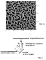
- FIG. 1a, FIG. 1b and FIG. 1c AFM images of examples which are well suited for the implementation of the securing method according to the present invention are shown on FIG. 1a, FIG. 1b and FIG. 1c , the areas scanned by AFM being different between, on the one hand, the first image and, on the other hand, the two last images.
- microstructures represented on these images respectively have well defined average lateral structure sizes of 0.9 ⁇ m, 3.4 ⁇ m and 6.0 ⁇ m.
- the vertical size is for all microstructures the same and about 100nm.
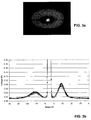
- a measuring method can be implemented with a sample Sa, at fixed angle, as schematically illustrated on FIG. 2 , where it appears that an incident laser beam IB leads to a central reflected beam RB as well as scattered additional beams SB more or less angled with respect to the central reflected beam RB.
- the resulting pattern can be made apparent by use of a projection screen Sc or can be measured by a detector array or a CCD camera.
- This method allows a simple verification of the average structure size and size distribution of samples.
- the incidence angle is not necessarily 45° as shown in FIG. 2 . It can be shallower or steeper or even perpendicular. Preferred are incidence angles between 0° (perpendicular) and 50°, especially preferred between 0° and 25°.
- a LED is used as light source instead of a laser.
- high-power LEDs can be used.
- the beam profile of such LED can be optimized by adequate lenses and/or apertures.
- the scattering pattern has the shape of one or several rings surrounding the central reflected spot.
- the diameter of the rings is correlated to the average lateral structure size d and the width of the rings to the size distribution w.
- the lower level of security verification is obtained if only the diameter of the ring and thus the average structure size d of the structures is analyzed or detected.
- the light beam should preferably have a spectral width smaller than 100nm to improve the scattering pattern legibility.
- Scattering of visible (wavelength 380nm - 780nm) or near infrared radiation (wavelength 780nm - 2000nm) is preferred.
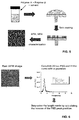
- FIG. 3a representing the scattering pattern as visible on the screen
- FIG. 3b represents two different line cuts through the ring center on either sides of the central peak.
- the difference in the intensity in the left and the right halves respectively is due to a tilt of the sample about a rotation axis symbolized by broken lines on FIG. 2 .
- the scattering pattern of FIG. 3a was formed on the basis of a defocused laser diode having a wavelength of 638nm and a spot size of 1220 ⁇ m on the sample surface.
- the distance of the laser to the sample was about 7 cm and the one between sample and projection screen about the same order.
- One possible method to extract the information from the scattering measurement is to identify the presence of a peak in a certain angular range or the peak position, e.g. by measuring the scattered intensity with a photodiode array.
- Another method is to record the whole shape of the scattered intensity curve and compare it with a reference data set in a memory. The width of the ring is defined by the distribution of the structure size.
- the higher level of security can be realized by measuring the speckle pattern in the ring which is a fingerprint of the local structure at the position of the security device which is measured.
- the light beam should preferably have a spectral width smaller than 100nm to improve the scattering pattern legibility.
- FIG. 4a representing the scattering pattern as visible on the screen
- FIG. 4b represents two different line cuts through the ring center.
- the difference in the intensity in the left and the right halves respectively is due to a tilt of the sample about a rotation axis symbolized by broken lines on FIG. 2 .
- the scattering pattern of FIG. 4a was formed on the basis of a focused laser diode having a spot diameter of 35 ⁇ m. Again, the distance of the laser to the sample was about 7cm and the one between sample and projection screen about the same order.
- the data can be recorded by a CCD-sensor, for example, or by one or more diode arrays.
- the data can be compared with a reference data previously recorded in a security reference database.
- the first above measuring embodiment offers a fast verification at lower security level, while the second embodiment offers high security verification at lower speed or higher tool costs.
- Suitable and preferred parameters of the scattering random or stochastic structures are listed in the table 1: Table I parameter Suitable range In particular suitable range preferred range Especially preferred range average structure size d 0.05 ⁇ m - 50 ⁇ m 0.5 ⁇ m - 50 ⁇ m 2 ⁇ m - 20 ⁇ m 3 ⁇ m - 12 ⁇ m size distribution w (PSD-FWHM) w ⁇ 2 ⁇ d -1 w ⁇ 2 ⁇ d -1 w ⁇ d -1 w ⁇ d -1 structure depth t 20nm - 2000nm 50nm - 2000nm 80nm - 500nm 80nm - 300nm ratio t / d ⁇ 5/1 ⁇ 2/1 ⁇ 1/4 ⁇ 1/10
- PSD Power Spectral Density, describing how the power of a signal or time series is distributed with frequency, and, FWHM, Full Width at Half Maximum.
- ratio t / d may be larger than 2/1 without going beyond the scope of the invention.
- the image of the scattering intensity looks very similar to a 2d Fourier transformation of the AFM image of the microstructures.
- an image analysis can be performed, as will be detailed later in connection with FIG. 6 .
- images obtained by other techniques like optical microscopes can be analyzed too.
- the scattering structures can be at the surface of a security device or at an interface located within it. The latter is possible if at least on one side of the interface the device material is transparent for the wavelength of the light source used in the verification tool. By transparent is meant that the material transmission should be larger than 75%, preferably larger than 90%.
- the micro- or nanostructures may be embossed in a polymer substrate or an embossable polymer layer on a substrate, the polymer possessing an index of refraction n of about 1.6 and an extinction coefficient close to zero.
- n index of refraction
- coatings which induce a step in the index of refraction and/or extinction coefficient are metals like Ag, Cu, Ni, Inconel and Au or dielectric materials like ZnS, TiO 2 , Cr 2 O 3 , AIN, Al 2 O 3 , HfO 2 , Nb 2 O 5 , Si 3 N 4 , SnN, Ta 2 O 5 , V 2 O 5 , WO 3 , or ZrO 2 or high index of refraction polymers like HRI721 and HRI751 (optimate).
- Stochastically arranged topology structures of the desired structure size and with the needed narrow size distribution can be manufactured by several ways like self assembly of polymer blend or block-co-polymer layers, or of bead layers made up of beads with a size in the range of 200nm up to 2000nm.
- phase separation of polymer blends this may occur when the system is brought from a stable state (single phase) to an unstable or metastable state (biphasic).
- the starting system is a binary polymer blend prepared in the one-phase region to form a homogeneous blend.
- the system is then subjected to a rapid change in temperature (temperature quench) to bring the blend from the one phase to the two phase region of its phase diagram.
- temperature quench a rapid change in temperature
- the second method uses a ternary system composed of two polymers and a common solvent for both polymers. At low polymer concentrations, the polymer chains are well dissolved and do not interact with neighboring polymer chains. Upon removal of the solvent, the polymer concentration increases until a threshold value above which the system phase separates. The system then undergoes phase separation until it is completely depleted of solvent.
- the polymer films made using the solvent quench approach are typically made by means of spin coating, as schematically illustrated on FIG. 5 .
- This technique is a convenient way to make thin polymer films.
- a polymer blend solution 10 comprising a polymer A, a polymer B and a solvent
- a thin liquid film first forms due to centrifugal forces. There is then a balance between the centrifugal and viscous forces which determine the thickness of the liquid film formed.
- the solvent evaporates, which leads to an increase in viscosity and initiates phase separation.
- solvent quench This process produces a rapid quench of the system which is frozen in a non-equilibrium state.
- solvent quench is employed.
- the solvent quench technique is more difficult to model since it involves additional phenomena to take into account: for instance solvent evaporation which induces an increase of polymer concentration at the free surface, leading to polymer concentration gradients through the depth of the film. It also leads to cooling of the interface (evaporative cooling) which may affect film formation.
- the solvent quench technique is widely used and many coating techniques (spin-coating, dip-coating, spray-coating) involve solvent quenching.
- Potential parameters to tune the structure size and morphologies include the composition of the polymer blend, the molecular weight of the polymers, the spin speed during spin coating, the concentration of the starting solution, the surface energy of the substrate, the evaporation rate of the solvent and humidity of the surrounding air.
- a well known system for polymer demixing is a blend of polystyrene (PS) and poly methyl methacrylate (PMMA). As illustrated on FIG. 5 , solutions of PS/PMMA (30/70)w/w dissolved in toluene were prepared and spin coated on clean silicon wafers.
- PS polystyrene
- PMMA poly methyl methacrylate
- the polystyrene phase may be removed by rinsing the sample in a solvent which is selective for PS, such as cyclohexane.
- a solvent which is selective for PS such as cyclohexane.
- the polymer concentration of the solution may be adjusted from 1 to 5 % w/v . It is already known that a higher concentration leads to thicker films and larger structures.
- FIG. 1a, FIG. 1b and FIG. 1c present respective AFM characterizations of respective samples obtained with three different polymer concentrations.
- the size of the structures increases when increasing the concentration of the solution.
- the morphology of the structures obtained is also clearly affected. In the case of the lowest concentration, bumps are obtained in contrast with the pores topography obtained for higher concentrations.
- the film thickness and the depth of the features is also different, from 30nm when using a 1% w/v solution, to 125 and 250nm with 3% w/v and 5% w/v solutions respectively.
- This analysis of a raw AFM image 20 allows a determination of the characteristic length-scale of the demixed structures to be conducted.
- a Fourier analysis may be performed and the power spectrum (2D iso PSD) is calculated on the basis of each of the above-mentioned images.
- the corresponding power spectrums may then be fitted with Gaussians (step A) and the peak positions (in the spatial-frequency domain) are measured.
- the length-scales of the structures may then be obtained by calculating the invert of the PSD peak positions (step B).
- the first described results were satisfying in terms of lateral structure sizes. However, the depth of the features was not controlled and the large features were much deeper than the small ones.
- the phase separation of the polymers strongly depends on their molecular weight. It is known from theory that an important parameter in the present context is the product ⁇ N, with ⁇ being the interaction parameter between the polymers and N the number of monomer block of the polymer chain.
- films obtained with low molecular weight polymers were relatively flat without significant nano-topographies, films obtained with higher molecular weights presented more interesting structures with very different structure sizes and morphologies.
- AFM and Image analysis were then performed to determine the depths and length-scales of the resulting structures. With optimized experimental conditions, surface structures with typical length-scales from 1 ⁇ m to 10 ⁇ m could be prepared.
- the depth of the structure was highly controlled and kept constant, around 110 ⁇ 10nm. This depth is preferred, though not limiting the scope of the invention, because it is enough to give good scattering results while easing the release of the embossing tool from the embossed substrate, in a later replication process. Indeed, if the structures are too deep, the probability that the embossed material sticks to the embossing tool, particularly in roll-to-roll embossing, rises distinctly. On the other hand a minimum structure depth is needed to get a scattering intensity which is high enough.
- the inventors developed strict protocols for the substrate cleaning as well as for the preparation and deposition of the polymer solutions.
- the arrangement of the structures on 3-inch samples is stochastically like a fingerprint, but the average structure size and/or distance and the distribution of the structure size is well defined.
- the structures may be transferred in an embossing or replication tool, such as Ni shim for roll-to-roll embossing or batch embossing or, tools for injection molding.
- an embossing or replication tool such as Ni shim for roll-to-roll embossing or batch embossing or, tools for injection molding.
- the micro- or nanostructures were transferred into such Ni-shims by an electroforming process preformed directly on the 3-inch spin-coated Si-wafers.
- a starting layer was deposited by thermal evaporation of approximately 50nm Silver.
- Other possible materials for the starting layer are Au or Ni.
- a 400 ⁇ m thick Ni layer was grown in an electroforming Ni-sulfamate bath (Technotrans EFM 2.02). It is a state-of-the-art process to manufacture batch production shims and embossing rolls for mass production in roll-to-roll embossing machines from such 3-inch shims. This process is widely used for the manufacturing of holograms or DOVIDs.
- the inventors used the 3-inch shims to hot-emboss the micro- or nanostructures in polymer substrate or foil.
- PC polycarbonate
- Suitable materials for the polymer substrate or foil are thermoplastic polymers.
- the polymer substrate or foil can be made of acrylonitrile butadiene styrene ABS, polycarbonate PC, polyethylene PE, polyetherimide PEI, polyetherketone PEK, poly(ethylene naphthalate) PEN, poly(ethylene therephtalate) PET, polyimide PI, poly(methyl methacrylate) PMMA, polyoxy-methylene POM, mono oriented polypropylene MOPP, polystyrene PS, polyvinyl chloride PVC and the like.
- the polymer substrate can be a carrier substrate coated with an embossable layer, e.g. an embossable polymer layer.
- such methods may be implemented on the basis of a coherent light beam having, preferably, a spectral width smaller than 100nm and being defocused so as to form a beam spot on the structures having a width larger than approximately 500 ⁇ m.
- the first above method may further comprise additional or alternate steps consisting in:
- An alternate more precise method would be to provide a coherent light beam having a spectral width smaller than 100nm and being focused so as to form a beam spot on the structures having a width smaller than approximately 500 ⁇ m, preferably smaller than 50 ⁇ m.
- the thus formed scattering ring pattern may play the role of a fingerprint to be compared with reference fingerprints recorded in a reference security database.
- the security device image data may be combined to further complementary information in the reference security database, such as a metadata of the secured valuable item which may include a set of data of commercial interest for the application that uses the anti-counterfeiting method (i.e. name of the owner, ownership history, authenticity check history, name of the expert who created the reference data, date and place of fabrication, etc..), or possibly a visual of the item.
- the recognition method may include additional checking operations related to this complementary information.
Landscapes
- Physics & Mathematics (AREA)
- General Physics & Mathematics (AREA)
- Health & Medical Sciences (AREA)
- General Health & Medical Sciences (AREA)
- Toxicology (AREA)
- Engineering & Computer Science (AREA)
- Computer Vision & Pattern Recognition (AREA)
- Credit Cards Or The Like (AREA)
- Image Analysis (AREA)
Claims (14)
- Sicherheitsvorrichtung zur Identifizierung oder Authentifizierung von Gütern, umfassend ein Substrat, das ein stochastisches Muster an einer freien Oberfläche oder an einer Grenzfläche desselben enthält und verwendet wird, um mindestens ein zu sicherndes Gut zu identifizieren, dadurch gekennzeichnet, dass:- das stochastische Muster Strukturen umfasst, die geprägt und zufällig an der freien Oberfläche oder an der Grenzfläche verteilt sind, wobei die Größe der Strukturen abstimmbar ist und sich diese in einer geregelten Tiefe in der freien Oberfläche oder der Grenzfläche des Substrats befinden; und- das stochastische Muster ein räumliches Leistungsdichtespektrum in 2D aufweist, das eine Spitze aufweist, die sich in einem Ring in der räumlichen Ebene des Leistungspektrums befindet, wobei der Ring einen Durchmesserwert aufweist, der mit der durchschnittlichen seitlichen Strukturgröße d korreliert, wobei der Ring eine Breite aufweist, deren Wert w kleiner als 2/d ist, wobei die Breite, wenn sie umgekehrt wird, mit einer Größenverteilung der Strukturen korreliert.
- Sicherheitsvorrichtung nach Anspruch 1, wobei die Strukturen derart angeordnet sind, dass sich ein ringförmiges Speckle-Streuungsmuster bildet.
- Sicherheitsvorrichtung nach Anspruch 1, wobei der Wert w kleiner als 1/d ist.
- Sicherheitsvorrichtung nach Anspruch 1, wobei die Strukturen Mikro- oder Nanostrukturen sind.
- Sicherheitsvorrichtung nach Anspruch 1, wobei die durchschnittliche seitliche Strukturgröße d in einem geeigneten Bereich enthalten ist, der ungefähr von 0,05 bis 50 µm, insbesondere geeignet von 0,5 bis 50 µm, bevorzugt von 2 bis 20 µm, weiter bevorzugt von 3 bis 12 µm reicht.
- Sicherheitsvorrichtung nach Anspruch 1, wobei die Strukturen eine Tiefe t aufweisen, die in einem geeigneten Bereich enthalten ist, der ungefähr von 20 bis 2000 nm, insbesondere geeignet von 50 bis 2000 nm, bevorzugt von 80 bis 500 nm, weiter bevorzugt von 80 bis 300 nm reicht.
- Sicherheitsvorrichtung nach Anspruch 6, wobei ein Verhältnis, das durch t/d definiert ist, kleiner als 5, insbesondere kleiner als 2, bevorzugt kleiner als 1/4, weiter bevorzugt kleiner als 1/10 ist.
- Sicherheitsvorrichtung nach Anspruch 1, wobei sich die Strukturen auf einer freien Oberfläche der Sicherheitsvorrichtung befinden.
- Sicherheitsvorrichtung nach Anspruch 1, wobei die Strukturen mit einer Materialschicht überzogen sind, die einen Transmissionswirkungsgrad von mindestens 75 %, bevorzugt von mindestens 90 %, für eine vordefinierte Lichtwellenlänge aufweist.
- Sicherheitsvorrichtung nach Anspruch 1, wobei die Strukturen mit einem Material überzogen sind, das aus der Gruppe gewählt wird, die Folgendes umfasst: Al, Ag, Cu, Ni, Au, Inconel, dielektrische Materialien wie etwa ZnS, TiO2, Cr2O3, AIN, Al2O3, HfO2, Nb2O5, Si3N4, SnN, Ta2O5, V2O5, WO3, ZrO2, Polymere mit hohem Brechungsindex wie etwa HRI721, HRI751.
- Verfahren zum Sichern eines Guts vor Fälschung, umfassend folgende Schritte:- Erzeugen einer Sicherheitsvorrichtung nach einem der Ansprüche 1 bis 10, umfassend Strukturen, die durch eine durchschnittliche Referenzstrukturgröße dR und einen Wert wR der Referenzverteilungsgröße gekennzeichnet sind,- Aufzeichnen der durchschnittlichen Strukturgröße dR und des Verteilungsgrößenwertes wR in einer Sicherheitsreferenzdatenbank,- wahlweises Auftragen der Sicherheitsvorrichtung auf eine Oberfläche des Guts,- Richten eines kohärenten Lichtstrahls auf mindestens einen Teil der Strukturen, um ein ringförmiges Speckle-Streuungsmuster zu bilden,- Messen des Durchmessers des ringförmigen Musters,- Berechnen einer durchschnittlichen Prüfstrukturgröße dv auf der Grundlage des Durchmessers,- Vergleichen der durchschnittlichen Prüfstrukturgröße dv mit durchschnittlichen Referenzstrukturgrößen dR, die in der Referenzsicherheitsdatenbank gespeichert sind,- Identifizieren oder Authentifizieren des Guts, falls die durchschnittliche Prüfstrukturgröße dv mit einer der durchschnittlichen Referenzstrukturgrößen dR, die in der Referenzsicherheitsdatenbank gespeichert sind, übereinstimmt.
- Verfahren nach Anspruch 11, ferner umfassend folgende Schritte:- Messen der Breite des ringförmigen Musters;- Berechnen eines Wertes wV der Prüfverteilungsgröße auf der Grundlage der Breite,- Vergleichen des Wertes wV der Prüfverteilungsgröße mit Werten wR der Referenzverteilungsgröße, die in der Referenzsicherheitsdatenbank gespeichert sind,- Identifizieren oder Authentifizieren des Guts, falls der Wert wV der Prüfverteilungsgröße mit einem der Werte wR der Referenzverteilungsgröße, die in der Referenzsicherheitsdatenbank gespeichert sind, übereinstimmt.
- Verfahren nach Anspruch 11 oder 12, wobei der kohärente Lichtstrahl eine Spektralbreite aufweist, die kleiner als 100 nm ist, und defokussiert ist, um einen Lichtpunkt auf den Strukturen zu bilden, der eine Breite aufweist, die größer als ungefähr 500 µm ist.
- Verfahren zum Sichern eines Guts vor Fälschung, umfassend folgende Schritte:- Erzeugen einer Sicherheitsvorrichtung nach einem der Ansprüche 1 bis 10, die Strukturen umfasst, die durch eine durchschnittliche Referenzstrukturgröße dR und einen Wert wR der Referenzverteilungsgröße, der kleiner als 2/dR ist, gekennzeichnet sind,- Erzeugen eines Streuungsringmusters als Referenz-Streuungsmusterfingerabdruck durch Streuen eines kohärenten Lichtstrahls, der eine Spektralbreite aufweist, die kleiner als 100 nm ist, und fokussiert ist, um einen Lichtpunkt auf den Strukturen zu bilden, der eine Breite aufweist, die kleiner als ungefähr 500 µm, bevorzugt kleiner als 50 µm ist,- Aufzeichnen des Referenz-Streuungsmusterfingerabdrucks in einer Sicherheitsreferenzdatenbank,- wahlweises Auftragen der Sicherheitsvorrichtung auf eine Oberfläche des Guts,- Richten eines kohärenten Lichtstrahls, der eine Spektralbreite aufweist, die kleiner als 100 nm ist, und fokussiert ist, um einen Lichtpunkt auf den Strukturen zu bilden, der eine Breite aufweist, die kleiner als ungefähr 500 µm, bevorzugt kleiner als 50 µm, ist, um die Sicherheitsvorrichtung zu prüfen, indem ein Streuungsringmuster als Prüf-Streuungsmusterfingerabdruck erzielt wird,- Vergleichen des Prüf-Streuungsmusterfingerabdrucks mit einem Referenz-Streuungsmusterfingerabdruck, der in der Referenzsicherheitsdatenbank gespeichert ist,- Identifizieren oder Authentifizieren des Guts, falls der Prüf-Streuungsmusterfingerabdruck mit einem der Referenz-Streuungsmusterfingerabdrücke, die in der Referenzsicherheitsdatenbank gespeichert sind, übereinstimmt.
Applications Claiming Priority (1)
| Application Number | Priority Date | Filing Date | Title |
|---|---|---|---|
| US91642007P | 2007-05-07 | 2007-05-07 |
Publications (3)
| Publication Number | Publication Date |
|---|---|
| EP1990779A2 EP1990779A2 (de) | 2008-11-12 |
| EP1990779A3 EP1990779A3 (de) | 2009-10-28 |
| EP1990779B1 true EP1990779B1 (de) | 2016-09-14 |
Family
ID=39673418
Family Applications (1)
| Application Number | Title | Priority Date | Filing Date |
|---|---|---|---|
| EP08155756.3A Not-in-force EP1990779B1 (de) | 2007-05-07 | 2008-05-07 | Sicherheitsvorrichtung zur Identifizierung oder Authentifizierung von Waren und Verfahren zur Sicherung von Waren mittels einer derartigen Sicherheitsvorrichtung |
Country Status (2)
| Country | Link |
|---|---|
| US (1) | US20090008925A1 (de) |
| EP (1) | EP1990779B1 (de) |
Families Citing this family (26)
| Publication number | Priority date | Publication date | Assignee | Title |
|---|---|---|---|---|
| US8171567B1 (en) | 2002-09-04 | 2012-05-01 | Tracer Detection Technology Corp. | Authentication method and system |
| RU2380750C2 (ru) | 2004-03-12 | 2010-01-27 | Инджениа Текнолоджи Лимитед | Способы и устройства для создания печатных изделий с возможностью установления их подлинности и с последующей их проверкой |
| JP4607947B2 (ja) | 2004-03-12 | 2011-01-05 | インジェニア・ホールディングス・(ユー・ケイ)・リミテッド | 真正性検証の方法、製品および機器 |
| GB2417592B (en) | 2004-08-13 | 2006-07-26 | Ingenia Technology Ltd | Authenticity verification of articles |
| EP1908027B1 (de) | 2005-07-27 | 2010-09-29 | Ingenia Holdings Limited | Verifikation der authentizität |
| GB2448245B (en) | 2005-12-23 | 2009-11-04 | Ingenia Holdings | Optical authentication |
| GB2460625B (en) * | 2008-05-14 | 2010-05-26 | Ingenia Holdings | Two tier authentication |
| GB2462029B (en) * | 2008-05-14 | 2010-08-25 | Ingenia Holdings | Tracking of an Article |
| US8153984B2 (en) | 2008-12-18 | 2012-04-10 | Eastman Kodak Company | Security system with different size emissive particles |
| GB2466311B (en) | 2008-12-19 | 2010-11-03 | Ingenia Holdings | Self-calibration of a matching algorithm for determining authenticity |
| US8659391B2 (en) * | 2009-08-18 | 2014-02-25 | Indian Institute Of Technology Madras | Multielement and multiproperty tagging |
| GB2476226B (en) | 2009-11-10 | 2012-03-28 | Ingenia Holdings Ltd | Optimisation |
| EP2333749B1 (de) | 2009-12-10 | 2013-10-16 | Universität Bayreuth | Künstlicher Fingerabdruck |
| DE102010047948A1 (de) * | 2010-10-08 | 2012-04-12 | Giesecke & Devrient Gmbh | Verfahren zum Prüfen eines optischen Sicherheitsmerkmals eines Wertdokuments |
| DE102011114410A1 (de) * | 2011-09-26 | 2013-03-28 | Giesecke & Devrient Gmbh | Verfahren zum Prüfen der Herstellungsqualität eines optischen Sicherheitsmerkmals eines Wertdokuments |
| EP2662806B1 (de) * | 2012-05-11 | 2014-05-14 | Sick AG | Optisches Kennzeichnungsmerkmal |
| US9903821B2 (en) | 2013-05-01 | 2018-02-27 | Indian Institute Of Technology Madras | Coated mesoflowers for molecular detection and smart barcode materials |
| FR3035819B1 (fr) | 2015-05-07 | 2021-04-30 | Honnorat Rech & Services | Papier authentifiable smartphone |
| US9952557B2 (en) * | 2015-05-11 | 2018-04-24 | Purdue Research Foundation | System for producing ultra-thin color phase hologram with metasurfaces |
| IL240872A (en) | 2015-08-27 | 2016-11-30 | Elbit Systems Land & C4I Ltd | A method and system for discovering object authenticity |
| US9418327B1 (en) | 2016-01-29 | 2016-08-16 | International Business Machines Corporation | Security key system |
| WO2019182051A1 (ja) | 2018-03-20 | 2019-09-26 | 凸版印刷株式会社 | 光学素子、および、認証体 |
| CN110618538A (zh) * | 2018-12-27 | 2019-12-27 | 武汉大学 | 一种微纳尺度的散斑制作方法 |
| WO2020162177A1 (ja) * | 2019-02-05 | 2020-08-13 | 東京応化工業株式会社 | 被認証物、認証システム、及び認証用媒体の生成方法 |
| CN112288941B (zh) * | 2020-03-06 | 2021-06-04 | 上海旺链信息科技有限公司 | 基于区块链的假币可疑程度测量系统及方法 |
| US11351811B2 (en) | 2020-05-29 | 2022-06-07 | International Business Machines Corporation | Optically-passive magnetic signature and identification feature with electromagnetic tamper detection |
Family Cites Families (12)
| Publication number | Priority date | Publication date | Assignee | Title |
|---|---|---|---|---|
| GB8812890D0 (en) | 1988-05-31 | 1988-07-06 | De La Rue Co Plc | Security device & methods & apparatus for verification |
| ATE142274T1 (de) * | 1989-05-22 | 1996-09-15 | Hoffmann La Roche | Verfahren zur markierung und zum nachweis von stoffen mit nukleinsäuren |
| GB2324065A (en) * | 1997-04-09 | 1998-10-14 | James Howard Slater | An identification code for banknotes or credit cards comprising a pattern of random beads |
| DE19853764A1 (de) | 1998-11-21 | 2000-05-31 | Simons Druck & Vertrieb Gmbh | System für die Sicherung und Kennzeichnung von Produkten unter Verwendung von Mikropartikeln |
| US6584214B1 (en) * | 1999-04-23 | 2003-06-24 | Massachusetts Institute Of Technology | Identification and verification using complex, three-dimensional structural features |
| US6744909B1 (en) * | 1999-08-19 | 2004-06-01 | Physical Optics Corporation | Authentication system and method |
| JP4048437B2 (ja) * | 2001-12-20 | 2008-02-20 | セイコーエプソン株式会社 | 偽造対策を施した記録物 |
| FR2849245B1 (fr) * | 2002-12-20 | 2006-02-24 | Thales Sa | Procede d'authentification et d'identification optique d'objets et dispositif de mise en oeuvre |
| GB2398759A (en) * | 2003-02-25 | 2004-09-01 | Univ Sheffield Hallam | An identification system using a random array of micro-lenses |
| DE102004002410B4 (de) | 2004-01-16 | 2008-09-18 | Infineon Technologies Ag | Identifizierungs- oder Authentifizierungsmedium |
| JP4607947B2 (ja) | 2004-03-12 | 2011-01-05 | インジェニア・ホールディングス・(ユー・ケイ)・リミテッド | 真正性検証の方法、製品および機器 |
| GB2417592B (en) * | 2004-08-13 | 2006-07-26 | Ingenia Technology Ltd | Authenticity verification of articles |
-
2008
- 2008-05-07 US US12/116,232 patent/US20090008925A1/en not_active Abandoned
- 2008-05-07 EP EP08155756.3A patent/EP1990779B1/de not_active Not-in-force
Also Published As
| Publication number | Publication date |
|---|---|
| EP1990779A2 (de) | 2008-11-12 |
| EP1990779A3 (de) | 2009-10-28 |
| US20090008925A1 (en) | 2009-01-08 |
Similar Documents
| Publication | Publication Date | Title |
|---|---|---|
| EP1990779A2 (de) | Sicherheitsvorrichtung zur Identifizierung oder Authentifizierung von Waren und Verfahren zur Sicherung von Waren mittels einer derartigen Sicherheitsvorrichtung | |
| US11951760B2 (en) | Information display medium and manufacturing method relating thereto | |
| US8824032B2 (en) | Security device with a zero-order diffractive microstructure | |
| EP1862827B2 (de) | Nanostrukturierter Diffraktionsfilter nullter Ordnung | |
| EP2021837B1 (de) | Optisch reflektierende oberflächen-reliefmikrostrukturen und herstellungsverfahren dafür | |
| AU2006202315B2 (en) | Covert security coating | |
| EP1990661B1 (de) | Isotroper Diffraktionsfilter nullter Ordnung | |
| US7787182B2 (en) | Diffractive optical security device | |
| CN101416079B (zh) | 结构体、结构体的形成方法、结构体形成装置、结构色以及衍射光读取方法和真伪判断方法 | |
| US20150360500A1 (en) | Security Device with Covert Images | |
| JP5163137B2 (ja) | 表示体及び表示体付き物品 | |
| KR20160083603A (ko) | 반투과성 편광이미지가 부가된 진위판정용 매체 |
Legal Events
| Date | Code | Title | Description |
|---|---|---|---|
| PUAI | Public reference made under article 153(3) epc to a published international application that has entered the european phase |
Free format text: ORIGINAL CODE: 0009012 |
|
| AK | Designated contracting states |
Kind code of ref document: A2 Designated state(s): AT BE BG CH CY CZ DE DK EE ES FI FR GB GR HR HU IE IS IT LI LT LU LV MC MT NL NO PL PT RO SE SI SK TR |
|
| AX | Request for extension of the european patent |
Extension state: AL BA MK RS |
|
| PUAL | Search report despatched |
Free format text: ORIGINAL CODE: 0009013 |
|
| AK | Designated contracting states |
Kind code of ref document: A3 Designated state(s): AT BE BG CH CY CZ DE DK EE ES FI FR GB GR HR HU IE IS IT LI LT LU LV MC MT NL NO PL PT RO SE SI SK TR |
|
| AX | Request for extension of the european patent |
Extension state: AL BA MK RS |
|
| 17P | Request for examination filed |
Effective date: 20100426 |
|
| AKX | Designation fees paid |
Designated state(s): AT BE BG CH CY CZ DE DK EE ES FI FR GB GR HR HU IE IS IT LI LT LU LV MC MT NL NO PL PT RO SE SI SK TR |
|
| 17Q | First examination report despatched |
Effective date: 20100722 |
|
| GRAP | Despatch of communication of intention to grant a patent |
Free format text: ORIGINAL CODE: EPIDOSNIGR1 |
|
| INTG | Intention to grant announced |
Effective date: 20160506 |
|
| GRAS | Grant fee paid |
Free format text: ORIGINAL CODE: EPIDOSNIGR3 |
|
| GRAA | (expected) grant |
Free format text: ORIGINAL CODE: 0009210 |
|
| AK | Designated contracting states |
Kind code of ref document: B1 Designated state(s): AT BE BG CH CY CZ DE DK EE ES FI FR GB GR HR HU IE IS IT LI LT LU LV MC MT NL NO PL PT RO SE SI SK TR |
|
| REG | Reference to a national code |
Ref country code: GB Ref legal event code: FG4D |
|
| REG | Reference to a national code |
Ref country code: CH Ref legal event code: EP |
|
| REG | Reference to a national code |
Ref country code: IE Ref legal event code: FG4D |
|
| REG | Reference to a national code |
Ref country code: CH Ref legal event code: NV Representative=s name: NOVAGRAAF INTERNATIONAL SA, CH |
|
| REG | Reference to a national code |
Ref country code: AT Ref legal event code: REF Ref document number: 829744 Country of ref document: AT Kind code of ref document: T Effective date: 20161015 |
|
| REG | Reference to a national code |
Ref country code: DE Ref legal event code: R096 Ref document number: 602008046253 Country of ref document: DE |
|
| REG | Reference to a national code |
Ref country code: LT Ref legal event code: MG4D |
|
| REG | Reference to a national code |
Ref country code: NL Ref legal event code: MP Effective date: 20160914 |
|
| PG25 | Lapsed in a contracting state [announced via postgrant information from national office to epo] |
Ref country code: LT Free format text: LAPSE BECAUSE OF FAILURE TO SUBMIT A TRANSLATION OF THE DESCRIPTION OR TO PAY THE FEE WITHIN THE PRESCRIBED TIME-LIMIT Effective date: 20160914 Ref country code: FI Free format text: LAPSE BECAUSE OF FAILURE TO SUBMIT A TRANSLATION OF THE DESCRIPTION OR TO PAY THE FEE WITHIN THE PRESCRIBED TIME-LIMIT Effective date: 20160914 Ref country code: NO Free format text: LAPSE BECAUSE OF FAILURE TO SUBMIT A TRANSLATION OF THE DESCRIPTION OR TO PAY THE FEE WITHIN THE PRESCRIBED TIME-LIMIT Effective date: 20161214 Ref country code: HR Free format text: LAPSE BECAUSE OF FAILURE TO SUBMIT A TRANSLATION OF THE DESCRIPTION OR TO PAY THE FEE WITHIN THE PRESCRIBED TIME-LIMIT Effective date: 20160914 |
|
| PG25 | Lapsed in a contracting state [announced via postgrant information from national office to epo] |
Ref country code: LV Free format text: LAPSE BECAUSE OF FAILURE TO SUBMIT A TRANSLATION OF THE DESCRIPTION OR TO PAY THE FEE WITHIN THE PRESCRIBED TIME-LIMIT Effective date: 20160914 Ref country code: NL Free format text: LAPSE BECAUSE OF FAILURE TO SUBMIT A TRANSLATION OF THE DESCRIPTION OR TO PAY THE FEE WITHIN THE PRESCRIBED TIME-LIMIT Effective date: 20160914 Ref country code: GR Free format text: LAPSE BECAUSE OF FAILURE TO SUBMIT A TRANSLATION OF THE DESCRIPTION OR TO PAY THE FEE WITHIN THE PRESCRIBED TIME-LIMIT Effective date: 20161215 Ref country code: SE Free format text: LAPSE BECAUSE OF FAILURE TO SUBMIT A TRANSLATION OF THE DESCRIPTION OR TO PAY THE FEE WITHIN THE PRESCRIBED TIME-LIMIT Effective date: 20160914 Ref country code: ES Free format text: LAPSE BECAUSE OF FAILURE TO SUBMIT A TRANSLATION OF THE DESCRIPTION OR TO PAY THE FEE WITHIN THE PRESCRIBED TIME-LIMIT Effective date: 20160914 |
|
| PG25 | Lapsed in a contracting state [announced via postgrant information from national office to epo] |
Ref country code: EE Free format text: LAPSE BECAUSE OF FAILURE TO SUBMIT A TRANSLATION OF THE DESCRIPTION OR TO PAY THE FEE WITHIN THE PRESCRIBED TIME-LIMIT Effective date: 20160914 Ref country code: RO Free format text: LAPSE BECAUSE OF FAILURE TO SUBMIT A TRANSLATION OF THE DESCRIPTION OR TO PAY THE FEE WITHIN THE PRESCRIBED TIME-LIMIT Effective date: 20160914 |
|
| REG | Reference to a national code |
Ref country code: FR Ref legal event code: PLFP Year of fee payment: 10 |
|
| PG25 | Lapsed in a contracting state [announced via postgrant information from national office to epo] |
Ref country code: PT Free format text: LAPSE BECAUSE OF FAILURE TO SUBMIT A TRANSLATION OF THE DESCRIPTION OR TO PAY THE FEE WITHIN THE PRESCRIBED TIME-LIMIT Effective date: 20170116 Ref country code: PL Free format text: LAPSE BECAUSE OF FAILURE TO SUBMIT A TRANSLATION OF THE DESCRIPTION OR TO PAY THE FEE WITHIN THE PRESCRIBED TIME-LIMIT Effective date: 20160914 Ref country code: BE Free format text: LAPSE BECAUSE OF FAILURE TO SUBMIT A TRANSLATION OF THE DESCRIPTION OR TO PAY THE FEE WITHIN THE PRESCRIBED TIME-LIMIT Effective date: 20160914 Ref country code: IS Free format text: LAPSE BECAUSE OF FAILURE TO SUBMIT A TRANSLATION OF THE DESCRIPTION OR TO PAY THE FEE WITHIN THE PRESCRIBED TIME-LIMIT Effective date: 20170114 Ref country code: BG Free format text: LAPSE BECAUSE OF FAILURE TO SUBMIT A TRANSLATION OF THE DESCRIPTION OR TO PAY THE FEE WITHIN THE PRESCRIBED TIME-LIMIT Effective date: 20161214 Ref country code: SK Free format text: LAPSE BECAUSE OF FAILURE TO SUBMIT A TRANSLATION OF THE DESCRIPTION OR TO PAY THE FEE WITHIN THE PRESCRIBED TIME-LIMIT Effective date: 20160914 Ref country code: CZ Free format text: LAPSE BECAUSE OF FAILURE TO SUBMIT A TRANSLATION OF THE DESCRIPTION OR TO PAY THE FEE WITHIN THE PRESCRIBED TIME-LIMIT Effective date: 20160914 |
|
| REG | Reference to a national code |
Ref country code: DE Ref legal event code: R097 Ref document number: 602008046253 Country of ref document: DE |
|
| PG25 | Lapsed in a contracting state [announced via postgrant information from national office to epo] |
Ref country code: IT Free format text: LAPSE BECAUSE OF FAILURE TO SUBMIT A TRANSLATION OF THE DESCRIPTION OR TO PAY THE FEE WITHIN THE PRESCRIBED TIME-LIMIT Effective date: 20160914 |
|
| PLBE | No opposition filed within time limit |
Free format text: ORIGINAL CODE: 0009261 |
|
| STAA | Information on the status of an ep patent application or granted ep patent |
Free format text: STATUS: NO OPPOSITION FILED WITHIN TIME LIMIT |
|
| PG25 | Lapsed in a contracting state [announced via postgrant information from national office to epo] |
Ref country code: DK Free format text: LAPSE BECAUSE OF FAILURE TO SUBMIT A TRANSLATION OF THE DESCRIPTION OR TO PAY THE FEE WITHIN THE PRESCRIBED TIME-LIMIT Effective date: 20160914 |
|
| 26N | No opposition filed |
Effective date: 20170615 |
|
| PG25 | Lapsed in a contracting state [announced via postgrant information from national office to epo] |
Ref country code: LU Free format text: LAPSE BECAUSE OF NON-PAYMENT OF DUE FEES Effective date: 20170531 |
|
| PG25 | Lapsed in a contracting state [announced via postgrant information from national office to epo] |
Ref country code: SI Free format text: LAPSE BECAUSE OF FAILURE TO SUBMIT A TRANSLATION OF THE DESCRIPTION OR TO PAY THE FEE WITHIN THE PRESCRIBED TIME-LIMIT Effective date: 20160914 |
|
| PG25 | Lapsed in a contracting state [announced via postgrant information from national office to epo] |
Ref country code: MC Free format text: LAPSE BECAUSE OF FAILURE TO SUBMIT A TRANSLATION OF THE DESCRIPTION OR TO PAY THE FEE WITHIN THE PRESCRIBED TIME-LIMIT Effective date: 20160914 |
|
| REG | Reference to a national code |
Ref country code: IE Ref legal event code: MM4A |
|
| PG25 | Lapsed in a contracting state [announced via postgrant information from national office to epo] |
Ref country code: LU Free format text: LAPSE BECAUSE OF NON-PAYMENT OF DUE FEES Effective date: 20170507 |
|
| PG25 | Lapsed in a contracting state [announced via postgrant information from national office to epo] |
Ref country code: IE Free format text: LAPSE BECAUSE OF NON-PAYMENT OF DUE FEES Effective date: 20170507 |
|
| REG | Reference to a national code |
Ref country code: FR Ref legal event code: PLFP Year of fee payment: 11 |
|
| PG25 | Lapsed in a contracting state [announced via postgrant information from national office to epo] |
Ref country code: MT Free format text: LAPSE BECAUSE OF NON-PAYMENT OF DUE FEES Effective date: 20170507 |
|
| REG | Reference to a national code |
Ref country code: AT Ref legal event code: UEP Ref document number: 829744 Country of ref document: AT Kind code of ref document: T Effective date: 20160914 |
|
| PG25 | Lapsed in a contracting state [announced via postgrant information from national office to epo] |
Ref country code: HU Free format text: LAPSE BECAUSE OF FAILURE TO SUBMIT A TRANSLATION OF THE DESCRIPTION OR TO PAY THE FEE WITHIN THE PRESCRIBED TIME-LIMIT; INVALID AB INITIO Effective date: 20080507 |
|
| PG25 | Lapsed in a contracting state [announced via postgrant information from national office to epo] |
Ref country code: CY Free format text: LAPSE BECAUSE OF NON-PAYMENT OF DUE FEES Effective date: 20160914 |
|
| PG25 | Lapsed in a contracting state [announced via postgrant information from national office to epo] |
Ref country code: TR Free format text: LAPSE BECAUSE OF FAILURE TO SUBMIT A TRANSLATION OF THE DESCRIPTION OR TO PAY THE FEE WITHIN THE PRESCRIBED TIME-LIMIT Effective date: 20160914 |
|
| PGFP | Annual fee paid to national office [announced via postgrant information from national office to epo] |
Ref country code: CH Payment date: 20200522 Year of fee payment: 13 Ref country code: DE Payment date: 20200525 Year of fee payment: 13 Ref country code: FR Payment date: 20200527 Year of fee payment: 13 |
|
| PGFP | Annual fee paid to national office [announced via postgrant information from national office to epo] |
Ref country code: GB Payment date: 20200522 Year of fee payment: 13 |
|
| PGFP | Annual fee paid to national office [announced via postgrant information from national office to epo] |
Ref country code: AT Payment date: 20200515 Year of fee payment: 13 |
|
| REG | Reference to a national code |
Ref country code: DE Ref legal event code: R119 Ref document number: 602008046253 Country of ref document: DE |
|
| REG | Reference to a national code |
Ref country code: CH Ref legal event code: PL |
|
| REG | Reference to a national code |
Ref country code: AT Ref legal event code: MM01 Ref document number: 829744 Country of ref document: AT Kind code of ref document: T Effective date: 20210507 |
|
| GBPC | Gb: european patent ceased through non-payment of renewal fee |
Effective date: 20210507 |
|
| PG25 | Lapsed in a contracting state [announced via postgrant information from national office to epo] |
Ref country code: LI Free format text: LAPSE BECAUSE OF NON-PAYMENT OF DUE FEES Effective date: 20210531 Ref country code: CH Free format text: LAPSE BECAUSE OF NON-PAYMENT OF DUE FEES Effective date: 20210531 Ref country code: AT Free format text: LAPSE BECAUSE OF NON-PAYMENT OF DUE FEES Effective date: 20210507 |
|
| PG25 | Lapsed in a contracting state [announced via postgrant information from national office to epo] |
Ref country code: GB Free format text: LAPSE BECAUSE OF NON-PAYMENT OF DUE FEES Effective date: 20210507 Ref country code: DE Free format text: LAPSE BECAUSE OF NON-PAYMENT OF DUE FEES Effective date: 20211201 |
|
| PG25 | Lapsed in a contracting state [announced via postgrant information from national office to epo] |
Ref country code: FR Free format text: LAPSE BECAUSE OF NON-PAYMENT OF DUE FEES Effective date: 20210531 |