EP1990796A2 - Flüssigkristallanzeige und Bildanzeigeverfahren dafür - Google Patents
Flüssigkristallanzeige und Bildanzeigeverfahren dafür Download PDFInfo
- Publication number
- EP1990796A2 EP1990796A2 EP08004713A EP08004713A EP1990796A2 EP 1990796 A2 EP1990796 A2 EP 1990796A2 EP 08004713 A EP08004713 A EP 08004713A EP 08004713 A EP08004713 A EP 08004713A EP 1990796 A2 EP1990796 A2 EP 1990796A2
- Authority
- EP
- European Patent Office
- Prior art keywords
- liquid crystal
- regions
- light
- emission luminance
- luminance
- Prior art date
- Legal status (The legal status is an assumption and is not a legal conclusion. Google has not performed a legal analysis and makes no representation as to the accuracy of the status listed.)
- Ceased
Links
- 239000004973 liquid crystal related substance Substances 0.000 title claims abstract description 144
- 238000000034 method Methods 0.000 title claims description 28
- 238000004364 calculation method Methods 0.000 claims abstract description 27
- 230000014509 gene expression Effects 0.000 claims abstract description 5
- 238000009826 distribution Methods 0.000 claims description 18
- 238000012937 correction Methods 0.000 abstract description 4
- 235000019557 luminance Nutrition 0.000 description 276
- 239000011159 matrix material Substances 0.000 description 17
- 238000010586 diagram Methods 0.000 description 10
- 238000005315 distribution function Methods 0.000 description 10
- 238000005192 partition Methods 0.000 description 9
- 238000006243 chemical reaction Methods 0.000 description 8
- 230000008569 process Effects 0.000 description 8
- 230000008859 change Effects 0.000 description 7
- 239000000758 substrate Substances 0.000 description 7
- 230000006870 function Effects 0.000 description 6
- 238000009792 diffusion process Methods 0.000 description 5
- 230000003287 optical effect Effects 0.000 description 5
- 230000007423 decrease Effects 0.000 description 4
- 239000007788 liquid Substances 0.000 description 4
- 238000000638 solvent extraction Methods 0.000 description 4
- 230000000694 effects Effects 0.000 description 3
- 230000009467 reduction Effects 0.000 description 3
- 230000003044 adaptive effect Effects 0.000 description 2
- 230000002238 attenuated effect Effects 0.000 description 2
- 239000003086 colorant Substances 0.000 description 2
- 230000006866 deterioration Effects 0.000 description 2
- 230000002349 favourable effect Effects 0.000 description 2
- 230000001965 increasing effect Effects 0.000 description 2
- 230000001678 irradiating effect Effects 0.000 description 2
- 230000004048 modification Effects 0.000 description 2
- 238000012986 modification Methods 0.000 description 2
- 239000000126 substance Substances 0.000 description 2
- QNRATNLHPGXHMA-XZHTYLCXSA-N (r)-(6-ethoxyquinolin-4-yl)-[(2s,4s,5r)-5-ethyl-1-azabicyclo[2.2.2]octan-2-yl]methanol;hydrochloride Chemical compound Cl.C([C@H]([C@H](C1)CC)C2)CN1[C@@H]2[C@H](O)C1=CC=NC2=CC=C(OCC)C=C21 QNRATNLHPGXHMA-XZHTYLCXSA-N 0.000 description 1
- 239000004593 Epoxy Substances 0.000 description 1
- 230000001154 acute effect Effects 0.000 description 1
- 230000002411 adverse Effects 0.000 description 1
- XAGFODPZIPBFFR-UHFFFAOYSA-N aluminium Chemical compound [Al] XAGFODPZIPBFFR-UHFFFAOYSA-N 0.000 description 1
- 229910052782 aluminium Inorganic materials 0.000 description 1
- 230000005540 biological transmission Effects 0.000 description 1
- 230000000593 degrading effect Effects 0.000 description 1
- 230000002542 deteriorative effect Effects 0.000 description 1
- 230000009977 dual effect Effects 0.000 description 1
- 230000002708 enhancing effect Effects 0.000 description 1
- 238000002474 experimental method Methods 0.000 description 1
- 230000012447 hatching Effects 0.000 description 1
- 238000004519 manufacturing process Methods 0.000 description 1
- 230000001360 synchronised effect Effects 0.000 description 1
- 238000013316 zoning Methods 0.000 description 1
Images











Classifications
-
- G—PHYSICS
- G09—EDUCATION; CRYPTOGRAPHY; DISPLAY; ADVERTISING; SEALS
- G09G—ARRANGEMENTS OR CIRCUITS FOR CONTROL OF INDICATING DEVICES USING STATIC MEANS TO PRESENT VARIABLE INFORMATION
- G09G3/00—Control arrangements or circuits, of interest only in connection with visual indicators other than cathode-ray tubes
- G09G3/20—Control arrangements or circuits, of interest only in connection with visual indicators other than cathode-ray tubes for presentation of an assembly of a number of characters, e.g. a page, by composing the assembly by combination of individual elements arranged in a matrix no fixed position being assigned to or needed to be assigned to the individual characters or partial characters
- G09G3/34—Control arrangements or circuits, of interest only in connection with visual indicators other than cathode-ray tubes for presentation of an assembly of a number of characters, e.g. a page, by composing the assembly by combination of individual elements arranged in a matrix no fixed position being assigned to or needed to be assigned to the individual characters or partial characters by control of light from an independent source
- G09G3/3406—Control of illumination source
- G09G3/342—Control of illumination source using several illumination sources separately controlled corresponding to different display panel areas, e.g. along one dimension such as lines
- G09G3/3426—Control of illumination source using several illumination sources separately controlled corresponding to different display panel areas, e.g. along one dimension such as lines the different display panel areas being distributed in two dimensions, e.g. matrix
-
- G—PHYSICS
- G02—OPTICS
- G02F—OPTICAL DEVICES OR ARRANGEMENTS FOR THE CONTROL OF LIGHT BY MODIFICATION OF THE OPTICAL PROPERTIES OF THE MEDIA OF THE ELEMENTS INVOLVED THEREIN; NON-LINEAR OPTICS; FREQUENCY-CHANGING OF LIGHT; OPTICAL LOGIC ELEMENTS; OPTICAL ANALOGUE/DIGITAL CONVERTERS
- G02F1/00—Devices or arrangements for the control of the intensity, colour, phase, polarisation or direction of light arriving from an independent light source, e.g. switching, gating or modulating; Non-linear optics
- G02F1/01—Devices or arrangements for the control of the intensity, colour, phase, polarisation or direction of light arriving from an independent light source, e.g. switching, gating or modulating; Non-linear optics for the control of the intensity, phase, polarisation or colour
- G02F1/13—Devices or arrangements for the control of the intensity, colour, phase, polarisation or direction of light arriving from an independent light source, e.g. switching, gating or modulating; Non-linear optics for the control of the intensity, phase, polarisation or colour based on liquid crystals, e.g. single liquid crystal display cells
- G02F1/133—Constructional arrangements; Operation of liquid crystal cells; Circuit arrangements
-
- G—PHYSICS
- G09—EDUCATION; CRYPTOGRAPHY; DISPLAY; ADVERTISING; SEALS
- G09G—ARRANGEMENTS OR CIRCUITS FOR CONTROL OF INDICATING DEVICES USING STATIC MEANS TO PRESENT VARIABLE INFORMATION
- G09G3/00—Control arrangements or circuits, of interest only in connection with visual indicators other than cathode-ray tubes
- G09G3/20—Control arrangements or circuits, of interest only in connection with visual indicators other than cathode-ray tubes for presentation of an assembly of a number of characters, e.g. a page, by composing the assembly by combination of individual elements arranged in a matrix no fixed position being assigned to or needed to be assigned to the individual characters or partial characters
- G09G3/34—Control arrangements or circuits, of interest only in connection with visual indicators other than cathode-ray tubes for presentation of an assembly of a number of characters, e.g. a page, by composing the assembly by combination of individual elements arranged in a matrix no fixed position being assigned to or needed to be assigned to the individual characters or partial characters by control of light from an independent source
- G09G3/3406—Control of illumination source
- G09G3/342—Control of illumination source using several illumination sources separately controlled corresponding to different display panel areas, e.g. along one dimension such as lines
-
- G—PHYSICS
- G09—EDUCATION; CRYPTOGRAPHY; DISPLAY; ADVERTISING; SEALS
- G09G—ARRANGEMENTS OR CIRCUITS FOR CONTROL OF INDICATING DEVICES USING STATIC MEANS TO PRESENT VARIABLE INFORMATION
- G09G3/00—Control arrangements or circuits, of interest only in connection with visual indicators other than cathode-ray tubes
- G09G3/20—Control arrangements or circuits, of interest only in connection with visual indicators other than cathode-ray tubes for presentation of an assembly of a number of characters, e.g. a page, by composing the assembly by combination of individual elements arranged in a matrix no fixed position being assigned to or needed to be assigned to the individual characters or partial characters
- G09G3/34—Control arrangements or circuits, of interest only in connection with visual indicators other than cathode-ray tubes for presentation of an assembly of a number of characters, e.g. a page, by composing the assembly by combination of individual elements arranged in a matrix no fixed position being assigned to or needed to be assigned to the individual characters or partial characters by control of light from an independent source
- G09G3/36—Control arrangements or circuits, of interest only in connection with visual indicators other than cathode-ray tubes for presentation of an assembly of a number of characters, e.g. a page, by composing the assembly by combination of individual elements arranged in a matrix no fixed position being assigned to or needed to be assigned to the individual characters or partial characters by control of light from an independent source using liquid crystals
- G09G3/3611—Control of matrices with row and column drivers
-
- G—PHYSICS
- G09—EDUCATION; CRYPTOGRAPHY; DISPLAY; ADVERTISING; SEALS
- G09G—ARRANGEMENTS OR CIRCUITS FOR CONTROL OF INDICATING DEVICES USING STATIC MEANS TO PRESENT VARIABLE INFORMATION
- G09G2320/00—Control of display operating conditions
- G09G2320/02—Improving the quality of display appearance
- G09G2320/0233—Improving the luminance or brightness uniformity across the screen
-
- G—PHYSICS
- G09—EDUCATION; CRYPTOGRAPHY; DISPLAY; ADVERTISING; SEALS
- G09G—ARRANGEMENTS OR CIRCUITS FOR CONTROL OF INDICATING DEVICES USING STATIC MEANS TO PRESENT VARIABLE INFORMATION
- G09G2320/00—Control of display operating conditions
- G09G2320/02—Improving the quality of display appearance
- G09G2320/0271—Adjustment of the gradation levels within the range of the gradation scale, e.g. by redistribution or clipping
-
- G—PHYSICS
- G09—EDUCATION; CRYPTOGRAPHY; DISPLAY; ADVERTISING; SEALS
- G09G—ARRANGEMENTS OR CIRCUITS FOR CONTROL OF INDICATING DEVICES USING STATIC MEANS TO PRESENT VARIABLE INFORMATION
- G09G2320/00—Control of display operating conditions
- G09G2320/02—Improving the quality of display appearance
- G09G2320/0285—Improving the quality of display appearance using tables for spatial correction of display data
-
- G—PHYSICS
- G09—EDUCATION; CRYPTOGRAPHY; DISPLAY; ADVERTISING; SEALS
- G09G—ARRANGEMENTS OR CIRCUITS FOR CONTROL OF INDICATING DEVICES USING STATIC MEANS TO PRESENT VARIABLE INFORMATION
- G09G2320/00—Control of display operating conditions
- G09G2320/04—Maintaining the quality of display appearance
- G09G2320/041—Temperature compensation
-
- G—PHYSICS
- G09—EDUCATION; CRYPTOGRAPHY; DISPLAY; ADVERTISING; SEALS
- G09G—ARRANGEMENTS OR CIRCUITS FOR CONTROL OF INDICATING DEVICES USING STATIC MEANS TO PRESENT VARIABLE INFORMATION
- G09G2320/00—Control of display operating conditions
- G09G2320/06—Adjustment of display parameters
- G09G2320/0626—Adjustment of display parameters for control of overall brightness
- G09G2320/0646—Modulation of illumination source brightness and image signal correlated to each other
-
- G—PHYSICS
- G09—EDUCATION; CRYPTOGRAPHY; DISPLAY; ADVERTISING; SEALS
- G09G—ARRANGEMENTS OR CIRCUITS FOR CONTROL OF INDICATING DEVICES USING STATIC MEANS TO PRESENT VARIABLE INFORMATION
- G09G2320/00—Control of display operating conditions
- G09G2320/06—Adjustment of display parameters
- G09G2320/0666—Adjustment of display parameters for control of colour parameters, e.g. colour temperature
-
- G—PHYSICS
- G09—EDUCATION; CRYPTOGRAPHY; DISPLAY; ADVERTISING; SEALS
- G09G—ARRANGEMENTS OR CIRCUITS FOR CONTROL OF INDICATING DEVICES USING STATIC MEANS TO PRESENT VARIABLE INFORMATION
- G09G2330/00—Aspects of power supply; Aspects of display protection and defect management
- G09G2330/02—Details of power systems and of start or stop of display operation
- G09G2330/021—Power management, e.g. power saving
-
- G—PHYSICS
- G09—EDUCATION; CRYPTOGRAPHY; DISPLAY; ADVERTISING; SEALS
- G09G—ARRANGEMENTS OR CIRCUITS FOR CONTROL OF INDICATING DEVICES USING STATIC MEANS TO PRESENT VARIABLE INFORMATION
- G09G2360/00—Aspects of the architecture of display systems
- G09G2360/14—Detecting light within display terminals, e.g. using a single or a plurality of photosensors
- G09G2360/145—Detecting light within display terminals, e.g. using a single or a plurality of photosensors the light originating from the display screen
-
- G—PHYSICS
- G09—EDUCATION; CRYPTOGRAPHY; DISPLAY; ADVERTISING; SEALS
- G09G—ARRANGEMENTS OR CIRCUITS FOR CONTROL OF INDICATING DEVICES USING STATIC MEANS TO PRESENT VARIABLE INFORMATION
- G09G2360/00—Aspects of the architecture of display systems
- G09G2360/16—Calculation or use of calculated indices related to luminance levels in display data
-
- G—PHYSICS
- G09—EDUCATION; CRYPTOGRAPHY; DISPLAY; ADVERTISING; SEALS
- G09G—ARRANGEMENTS OR CIRCUITS FOR CONTROL OF INDICATING DEVICES USING STATIC MEANS TO PRESENT VARIABLE INFORMATION
- G09G3/00—Control arrangements or circuits, of interest only in connection with visual indicators other than cathode-ray tubes
- G09G3/20—Control arrangements or circuits, of interest only in connection with visual indicators other than cathode-ray tubes for presentation of an assembly of a number of characters, e.g. a page, by composing the assembly by combination of individual elements arranged in a matrix no fixed position being assigned to or needed to be assigned to the individual characters or partial characters
- G09G3/34—Control arrangements or circuits, of interest only in connection with visual indicators other than cathode-ray tubes for presentation of an assembly of a number of characters, e.g. a page, by composing the assembly by combination of individual elements arranged in a matrix no fixed position being assigned to or needed to be assigned to the individual characters or partial characters by control of light from an independent source
- G09G3/36—Control arrangements or circuits, of interest only in connection with visual indicators other than cathode-ray tubes for presentation of an assembly of a number of characters, e.g. a page, by composing the assembly by combination of individual elements arranged in a matrix no fixed position being assigned to or needed to be assigned to the individual characters or partial characters by control of light from an independent source using liquid crystals
- G09G3/3611—Control of matrices with row and column drivers
- G09G3/3648—Control of matrices with row and column drivers using an active matrix
Definitions
- the present invention relates to a liquid crystal display device having a backlight device, and to an image display method for displaying an image signal while controlling light emission of the backlight device.
- a backlight device is provided, for example, on the back of the liquid crystal panel.
- the liquid crystal in the panel is switched between an OFF state and an ON state according to applied voltage.
- the liquid crystal display device drives, as electric shutters, multiple pixels within the liquid crystal panel, by controlling the voltage applied to each of the multiple pixels. An image forms by this control of transmission of light from the backlight through the panel.
- a cold cathode tube (CCFL (cold cathode fluorescent lamp)) has heretofore been mainly used as a backlight in a backlight device.
- CCFL cold cathode fluorescent lamp
- a large share of power consumption by a conventional liquid crystal display device is for the backlight device. Therefore, a liquid crystal display device has a problem of needing a large power consumption in order to keep the backlight in the constant lighting state.
- various methods have been proposed wherein a light emitting diode (LED) is used as a backlight. The emission luminance of the LED changes according to the brightness of the image signal.
- LED light emitting diode
- Non-patent Document 1 refers to this technique as "adaptive dimming.”
- the multiple divided regions of the backlight device are each partitioned by a light shielding wall.
- the emission luminance of each region is controlled entirely independently according to the image signal strength for each respective region.
- the LEDs vary in brightness and color, device by device, for their principal wavelength. The degree of such variation differs among colors of red (R), green (G) and blue (B). For this reason, when the multiple regions of the backlight device are completely separated from each other, the brightness and color varies among the regions. As a result, this produces the problem that an image displayed on the liquid crystal panel differs from an original image.
- the brightness and light emission wavelength of an LED has a temperature dependence.
- an R LED emits less amounts of light with an increase in device temperature, and also experiences a large change of wavelength.
- the R, G and B devices have different properties in terms of age deterioration. For this reason, the foregoing problem is particularly acute due to change in temperatures of the LED devices and due to age deterioration of the LED devices.
- Non-patent Document 1 In the configuration wherein the regions are completely separated from each other, it is difficult to determine the locations of adjacent regions of a particular pixel located above a boundary between the adjacent regions. This is because the manufacturing accuracy of the backlight device is far lower than that of the liquid crystal panel. For this reason, the configuration described in Non-patent Document 1 is not very useful.
- power consumption can be reduced by employing a configuration wherein a backlight device is divided into multiple regions, and in which the emission luminance of a backlight for each region is controlled according to the brightness of an image signal.
- An aspect of the invention provides a liquid crystal display device that comprises: a liquid crystal panel for displaying image signals; a backlight device disposed on the back side of the liquid crystal panel, the panel divided into multiple regions, and having light sources respectively in the multiple regions, the light source irradiate the liquid crystal panel with emitted light, and the backlight device having a structure in which light emitted from each of the light sources of the multiple regions is allowed to leak into regions other than the respective region of the concerned light source; a maximum gradation detector for detecting, at intervals of a predetermined unit time, a first maximum gradation of each regional image signals displayed on multiple regions of the liquid crystal panel respectively corresponding to the multiple regions of the backlight device; an image gain calculator for obtaining, as a gain for the regional image signal, a value equivalent to a value obtained by dividing a second maximum gradation by the first maximum gradation, the second maximum gradation being a possible maximum gradation of the regional image signal and determined according to the number of bits of the regional image signal;
- the backlight device is divided into multiple regions and the emission luminance of a backlight for each region is controlled by the strength of an image signal.
- the emission luminance of a backlight for each region is controlled by the strength of an image signal.
- FIG. 1 is a block diagram showing an entire configuration of the liquid crystal display device of the first embodiment.
- an image signal to be displayed on liquid crystal panel 34 in liquid module unit 30, which will be described later, is supplied to a maximum gradation detector 11 and frame memory 13 in image signal processor 10.
- backlight device 35 is divided into a plurality of regions, and liquid crystal panel 34 is divided into a plurality of regions so that these divided regions, respectively, correspond to the divided regions of backlight device 35, whereby luminance of the backlight (amount of light) is controlled in every region of liquid crystal panel 34.
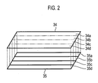
- Fig. 2 is a view showing an example of region divisions of liquid crystal panel 34 and of backlight device 35, while showing a schematic perspective view of a relationship between regions of liquid crystal panel 34 and regions of backlight device 35.
- liquid crystal panel 34 and backlight device 35 are arranged so that liquid crystal panel 34 and backlight device 35 are spaced away from each other.
- backlight device 35 is divided in regions 35a to 35d, and each of regions 35a to 35d have backlights, respectively.
- Liquid crystal panel 34 includes a plurality of pixels consisting of, for example, 1920 pixels in the horizontal direction, and 1080 in the vertical direction.
- Liquid crystal panel 34 has a plurality of pixels divided into regions 34a to 34d so that these regions 34a to 34d can correspond to regions 35a to 35d of backlight device 35.
- liquid crystal panel 34 is one-dimensionally divided into four regions, i.e., regions 34a to 34d, in a vertical direction, one region contains 270 pixels in the vertical direction.
- the pixels, concluded in each of four regions 34a to 34d, may naturally be scattered in the vertical direction.
- Liquid crystal panel 34 is not physically divided into regions 34a to 34d, but multiple regions (here, regions 34a to 34d) are set on liquid crystal panel 34.
- Image signals to be supplied to liquid crystal panel 34 correspond to multiple regions set on liquid crystal panel 34, and processed as image signals for respective regions, which are respectively displayed on the plurality of regions.
- Image signals, which are supplied to liquid crystal panel 34 are processed as respective image signals corresponding to the multiple regions, which are to be displayed on the multiple regions set on liquid crystal panel 34.
- the luminances of the backlights are individually controlled.
- liquid crystal panel 34 is vertically divided into four regions.
- backlight device 35 also is vertically divided into four regions. These regions may be further divided (sectioned). Further, as will be described later, liquid crystal panel 34 is divided in both vertical and horizontal directions. Corresponding to this division, backlight device 35 also may be divided in both vertical and horizontal directions. Preferably the number of divided (sectioned) regions are larger and partitioning (sectioning) in both vertical and horizontal directions is better than partitioning (zoning) in the horizontal direction only.
- Fig. 1 is described, with four vertically divided regions shown in Fig. 2 as an example.
- maximum gradation detector 11 detects maximum gradations of each image signal displayed on respective regions 34a to 34d of liquid crystal panel 34.
- a maximum gradation is detected for every frame of an image signal, but a maximum gradation may be detected for every two frame depending on circumstances. In either case, the detector may detect the maximum gradation for every unit of time determined in advance.
- Each data point, which represents a maximum gradation on regions 34a to 34d as detected by maximum gradation detector 11, is supplied to gain calculator 12 and non-uniformization processor 21.
- Calculator 12 within image signal processor 10 and processor 21 is within backlight luminance controller 20.
- Image gain calculator 12 calculates a gain, by which image signals to be displayed on regions 34a to 34d are multiplied, in the following manner.
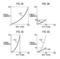
- Figs. 3A to 3D describe a gain calculation process which is operated in the image gain calculator 12. For every image signal supplied to each of regions 34a to 34d of liquid crystal panel 34, a gain to be multiplied to an image signal is obtained. Accordingly, a gain calculation, as described below, is performed on each image signal supplied to regions 34a to 34d.
- an input signal (image signal) indicated on the horizontal axis is represented in 8-bit, 0 to 255 gradation.
- display luminance (display gradation) of liquid crystal panel 34 indicated on the vertical axis takes a value from 0 to 255 for the sake of simplicity, without consideration of transmissivity of liquid crystal panel 34.
- Bit number of the image signal is not limited to 8-bits, but may be for example, 10-bits.
- a curve Cv1 in Fig. 3A shows how display luminance for an image signal having gradation of 0 to 255 is presented on liquid crystal panel 34.
- curve Cv1 is represented by a curve in which y is a function of x to the power of 2.2 to 2.4.
- This curve usually is referred to as a gamma curve with a gamma of 2.2 to 2.4.
- the curve in Fig. 3A may not be represented by the gamma curve Cv1, according to the kind of the liquid crystal panel 34.
- an image signal having characteristics indicated by curve Cv3 differs from an initial signal having characteristics indicated by curve Cv2 of Fig. 3B .
- backlights consume unnecessary power.
- the light emission luminance of the backlights is set to approximately 1/4.5 of the maximum luminance, so that the curve Cv3, with a display luminance of 0 to 255 can become curve Cv4 with display luminance of 0 to 56.
- an image signal having characteristics indicated by the curve Cv4 substantially becomes equivalent to that having characteristics indicated by curve Cv2, and power consumption of the backlights is reduced.
- Gmax1 denotes a maximum gradation of an image signal displayed on each of regions 34a to 34d within one frame period
- Gmax0 denotes a possible maximum gradation of the image signal.
- the achievable maximum gradation is determined according to the number of bits of image signals.
- image gain calculator 12 sets Gmax0/Gmax1 for each of regions 34a to 34d as a gain to be multiplied to an image signal being displayed on each of regions 34a to 34d.
- Gmax1/Gmax0 which is an inverse number of the gain Gmax0/Gmax1, is used to control luminance of the backlights in backlight luminance controller 20.
- a gain for each one of regions 34a to 34d calculated by image gain calculator 12 is inputted into multiplier 14.
- Multiplier 14 multiplies gains respectively to image signals being outputted from frame memory 13, and outputs the multiplied image signals for display on regions 34a to 34d.
- Image signals outputted from multiplier 14 are supplied to timing controller 31 in liquid module unit 30.
- Liquid crystal panel 34 includes multiple pixels 341 as previously described.
- Data signal line driver 32 is connected to data signal lines of pixels 341, and gate signal line driver 33 is connected to gate signal lines.
- An image signal inputted to timing controller 31 is supplied to data signal line driver 32.
- Timing controller 31 controls timings at which image signals are written on liquid crystal panel 34, by data signal line driver 32 and gate signal line driver 33.
- Pixel data constituting respective lines of image signals inputted in data signal line driver 32 are written in sequence in pixels of respective lines one by one through the driving of the gate signal lines by gate signal line driver 33. Thus, respective frames of image signals are displayed on liquid crystal panel 34 in sequence.
- Backlight device 35 is disposed on the back side of liquid crystal panel 34.
- a direct-type backlight device and/or a light-guiding plate type backlight device may be used as backlight device 35.
- the direct-type backlight device is disposed directly below liquid crystal panel 34.
- the light-guiding plate type backlight device light emitted from a backlight is made incident onto a light-guiding plate so as to irradiate liquid crystal panel 34.
- Backlight device 35 is driven by backlight driver 36.
- power is supplied from power source 40 to cause the backlight to emit light.
- power source 40 supplies power to circuits which need power.
- Liquid module unit 30 includes temperature sensor 37, which detects the temperature of backlight device 35, and color sensor 38, which detects the color temperature of light emitted from backlight device 35.
- FIG. 4 is a view showing an embodiment wherein backlight device 35 is divided into four regions along the longitudinal to vertical directions.
- backlight device 35A a first configuration example of backlight device 35 shown in Fig. 4
- backlight device 35B a second configuration example of backlight device 35 shown in Fig. 5
- Backlight device 35 is a collective term for backlight device 35A, backlight device 35B and other configuration.
- Fig. 4A is a top view of backlight device 35A
- Fig. 4B is a sectional view showing a state in which backlight device 35A is vertically cut.
- backlight device 35A has a configuration in which light source 352 for the backlight is horizontally arranged in and attached to rectangular housing 351 having a predetermined depth.
- Light source 352 is, for example, an LED.
- Backlight device 35A is divided into regions 35a to 35d with partition walls 353.
- Partition walls 353 protrude from the bottom surface of housing 351 to the predetermined portion higher than the uppermost surface (vertexes) of light sources 352. Inner sides of housing 351 and surfaces of partition wall 353 are covered with reflective sheets.
- Diffusion plate 354 diffusing light is mounted on an upper part of housing 351.
- Three optical sheets and their like 355 are mounted on diffusion plate 354 for example.
- Optical sheets and their like 355 are formed by combining multiple sheets such as a diffusion sheet, a prism sheet, and a brightness enhancement film, which is referred to as a DBEF (Dual Brightness Enhancement Film).
- DBEF Double Brightness Enhancement Film
- Each top surface of partition walls 353, covered with reflective sheet, does not reach diffusion plate 354, so that regions 35a to 35d are not separated, and are not completely independent from each other. That is, backlight device 35A has a structure in which light emission from each light source 352 of regions 35a to 35d is allowed to leak to other regions. As described later, in the first embodiment, the amount of light leaked from regions 35a to 35d to other regions is considered, allowing control of the luminances of the lights emitted from regions 35a to 35d.
- Fig. 5 is a view showing backlight device 35B, which is a second configuration example of backlight device 35 in the case where liquid crystal panel 34 is divided into four regions in the vertical direction and, further, divided into four regions in the horizontal direction, i.e., in the case where liquid crystal panel 34 is divided into sixteen regions in two dimension.
- Fig. 5A is a top view of backlight device 35B;
- Fig. 5B is a sectional view showing backlight device 35B cut in the vertical direction.
- Fig. 5C is a sectional view showing backlight device 35B cut in the horizontal direction.
- Fig. 5B shows backlight device 35B cut along the left-end partition wall in Fig. 5A.
- Fig. 5C shows backlight device 35B cut along the top-end partition wall in Fig. 5A .
- Housing 351 is divided into sixteen regions, regions 35a1 to 35a4, 35b1 to 35b4, 35c1 to 35c4, and 35d1 to 35d4, with partition walls 353 in the horizontal and vertical directions.
- Backlight device 35B has a structure in which light emits from each of light sources 352 in regions 35a1 to 35a4, 35b1 to 35b4, 35c1 to 35c4, and 35d1 to 35d4 and is allowed to leak to other regions.
- the amount of light leakage from respective regions 35a1 to 35a4, 35b1 to 35b4, 35c1 to 35c4, and 35d1 to 35d4 to other regions is considered so that luminances of light from regions 35a1 to 35a4, 35b1 to 35b4, 35c1 to 35c4, and 35d1 to 35d4 are controlled.
- a LED is a highly directional light source. Accordingly, when a LED is used for light source 352, the heights of partition walls 353 covered with reflective sheets may be lower than that shown in Figs. 4 and 5 , and may be removed depending on the situation.
- Dome-like lenses may cover elements of light sources 352 so that the same effects can occur as that caused by partition walls 353.
- light sources other than LEDs such as CCFLs and external electrode fluorescent lamps (EEFLs) may be used as light sources for the backlight.
- CCFLs and external electrode fluorescent lamps (EEFLs) may be used as light sources for the backlight.
- EEFLs external electrode fluorescent lamps
- an LED is still preferable as light source 352 in the first embodiment since it is easy to control light emission luminance and the light emitting area thereof.
- the specific configuration of backlight device 35 is not limited to those shown in Figs. 4 and 5 .
- light sources 352 shown in Figs. 4 and 5 are configured as follows.
- LED 357G of G, LED 357R of R, LED 357B of B, and LED 357G of G are mounted on substrate 356 in this order.
- Substrate 356 is, for example, an aluminum substrate or an epoxy substrate.
- Each of light sources 352, shown in Figs. 4 and 5 is configured by aligning multiple light sources 352 of Fig. 6A .
- LED 357R of R, LED 357G of G, LED 357B of B, and LED 357G of G are mounted on substrate 356 in a rhombic shape.
- Each of light sources 352, shown in Figs. 4 and 5 is configured by aligning multiple light sources 352 of Fig. 6B .
- a third configuration example of light source 352 shown in Fig. 6C twelve LED chips, each portion of which integrally includes LED 357R of R, LED 357G of G, and LED 357B of B, are mounted on substrate 356.
- Each of light sources 352, shown in Figs. 4 and 5 is configured by aligning multiple light sources 352 of Fig. 6C .
- two LED357Ws of white (W) are mounted on substrate 356.
- Each of light sources 352, shown in Figs. 4 and 5 is configured by aligning multiple light sources 352 of Fig. 6D .
- LED357Ws are in two types, one in which a yellow fluorescent substance is excited by a light irradiated from an LED of B to generate white light, and a second in which fluorescent substances of R, G, and B are exited by ultraviolet rays irradiated from an LED to generate white light. Any of the above two types can be employed.
- backlight luminance controller 20 includes light emission luminance calculator 22, white balance adjustor 23, and PWM timing generator 24.
- backlight device 35 will be described as backlight device 35A shown in Fig. 4 .
- the maximum luminance of a backlight as Bmax
- the light emission luminance of each of backlight regions 35a to 35d of backlight device 35 may be obtained by multiplying Gmax1/Gmax0, which is obtained for each of regions 34a to 34d, by maximum luminance Bmax.
- non-uniformization processor 21 obtains luminances B1 to B4 that the backlines of regions 35a to 35d are expected to emit.
- Calculated light emission luminances B1 to B4 are not for the light right above light sources 352 when the backlight light sources emit light, but are from lights emitted from backlight device 35 itself. That is, in the configuration examples of Figs. 4 and 5 , light emission luminances B1 to B4 are over optical sheets or the like 355. Incidentally, the calculated light emission luminance from a light that is expected to emit from one region of backlight device 35 is collectively referred to as B. In the following description, it is assumed that luminance distributions of light emitted from regions 35a to 35d of the backlight device are uniform within each region. However, in some case the luminance distribution is not uniform in one region. Such case, luminance at any arbitrary point within one region may be any of light emission luminances B1 to B4.
- non-uniformization processor 21 multiplies the calculated light emission luminances B1 to B4 by non-uniformization coefficients p1 to p4 so that the light emission luminances of lights really emitted from the regions 35a to 35d are set as p1B1, p2B2, p3B3, and p4B4.
- coefficients p1 to p4 is greater than 0, and equal to 1 or less.
- the inventors have found the following relationship between the quality of images displayed on liquid crystal panel 34 and the conditions where the backlights emit. Specifically, the image quality is higher when the backlights emit lights with slightly lower light emission luminances than calculated ones, along a periphery of the screen of liquid crystal panel 34.
- light emission luminances B1 and B4 from regions 35a and 35d equivalent to upper and lower parts of the screen may be set lower than those B2 and B3 from regions 35b and 35c. More specifically, as an example, p1 is set to 0.8; p2 and p3 are set to 1; and p4 is set to 0.8.
- non-uniformization processor 21 allow reduction of power consumption by backlight device 35, while rather enhancing the quality of images displayed on liquid crystal panel 34, and not degrading the quality thereof.
- the coefficients p1 to p4 be set to 0.8 to 1.0.
- the coefficient p to be multiplied to each light emission luminance of backlights at a screen center is set to 1.0, and that to each light emission luminance at a periphery of the screen is set to a value in a range having a lower bound of 0.8.
- liquid crystal panel 34 and backlight device 35 are divided into regions in two dimensions.
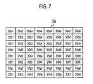
- liquid crystal panel 34 and backlight device 35 are divided into eight regions horizontally and vertically respectively, i.e., they are divided in two dimensions into sixty-four regions.
- backlight device 35 has regions 35a1 to 35a8, 35b1 to 35b8, 35c1 to 35c8, 35d1 to 35d8, 35e1 to 35e8, 35f1 to 35f8, 35g1 to 35g8, and 35h1 to 35h8.
- liquid crystal panel 34 is partitioned into sixty-four regions that correspond to the sixty-four regions of backlight device 35.
- Fig. 8A illustrates an example wherein coefficient p is multiplied to each of calculated light emission luminances of respective regions 35c1 to 35c8, 35d1 to 35d8, 35e1 to 35e8, 35f1 to 35f8, which correspond to four rows of the backlight device 35 in the central part thereof in the vertical direction and wherein each indicate eight regions in the horizontal direction.
- the left and right directions show regions of the screen of liquid crystal panel 34 in the horizontal direction.
- the left-hand side corresponds to the left end of the screen, and the right-hand side corresponds to the right end thereof.
- coefficient p is set to 1; regions on the left and right sides are set to 0.9; and regions on the left and right ends are set to 0.8.
- coefficient p is set to decrease gradually in sequence from the central part, where the coefficient p is 1, to the left and right ends. At this time, it is preferable that coefficient p be laterally symmetric with respect to the middle in the horizontal direction.
- coefficient p has been set to 1 for the central four regions.
- coefficient p may be set so that the coefficient p takes the value of 1 for the central two regions.
- coefficient p decreases in sequence from a value less than 1, to 0.8, for regions from the left and right sides of these two regions towards the left and right ends.
- a region may have a coefficient p of 1. Characteristics of coefficient p in the horizontal direction may be further adjusted to provide the most favorable image quality on a real screen.
- Fig. 8B is a view showing an example of a coefficient p that is multiplied to calculate each light emission luminance of respective regions 35a3 to 35h3, 35a4 to 35h4, 35a5 to 35h5, and 35a6 to 35h6, which correspond to four columns of the backlight device 35 in the central part thereof in the horizontal direction and which each indicate eight regions in the vertical direction.
- the left and right directions show the vertical direction of the screen of liquid crystal panel 34.
- the left-hand side corresponds to an upper end of the screen, and the right-hand side corresponds to a lower end thereof.
- coefficient p is set to 1.
- regions on the upper and lower sides thereof are set to 0.9; and regions on the upper and lower ends are set to 0.8.
- coefficient p be set to decrease gradually in sequence from the central part, where the coefficient p is 1, to the upper and lower ends. At this time, it is preferable that coefficient p be symmetric with respect to the middle in the vertical direction toward the upper and lower ends.
- coefficient p has been set to 1 for the central four regions. However, coefficient p may be set to take the value of 1 for the central two regions. In this instance, coefficient p decreases in sequence from a value less than 1, to 0.8 for regions from the upper and lower sides of these two regions toward the upper and lower ends.
- one region may have a coefficient p of 1. Characteristics of the coefficient p in the vertical direction may be adjusted to provide a most favorable image quality on a real screen. Incidentally, the characteristics of coefficient p in the horizontal and vertical directions may differ from each other.
- Controller 50 supplies coefficient p for use in non-uniformization processor 21. Controller 50 can be configured by a microcomputer, and coefficient p can be arbitrarily varied. Data that indicate each light emission luminance is inputted into light emission luminance calculator 22, and the luminance of light that each light source 352 is expected to emit is calculated as follows. A calculation method of luminance of light that each of light sources 352 is expected to emit will be described, in the case where backlight device 35 represents backlight device 35A having regions 35a to 35d. Light emission luminances of lights to be actually emitted from regions 35a to 35d are represented by p 1 B 1 , P 2 B 2 , P 3 B 3 , and p 4 B 4 respectively.
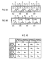
- Fig. 9A shows a sectional view of Fig. 4B in a laid flat position.
- optical sheets or their like 355 are omitted.
- B' with "'” represents a light emission luminance value on which a non-uniformization process is performed by non-uniformization processor 21, while B without “'” represents a light emission luminance value on which a non-uniformization process is not performed.
- B O1 , B O2 , B O3 , and B O4 represent luminances directly above light sources 352 of regions 35a to 35d respectively, assuming that each light source 352 emits a light individually.
- backlight device 35 has a structure wherein light that emits from each of light sources 352 of regions 35a to 35d is allowed to leak to other regions, so that the light emission luminances B 1 ', B 2 ', B 3 ', and B 4 ' and the light emission luminances B O1 , B O2 , B O3 , and B O4 are respectively not identical.
- the small light attenuation due to the presence of diffusion plate 354 and optical sheets or their like 355 can be ignored.
- the light emission luminance directly above light sources 352 when light source 352 on one region of backlight device 35 individually emits a light collectively are referred to as B O .
- each light from corresponding light sources 352 leaks to adjacent regions, while showing up as light leakage L1 with a the light emission luminance that is k multiplied by a corresponding B O1 , B O2 , B O3 , or B O4 .
- k represents an attenuation coefficient when light leaks. The value of k is greater than 0 and less than 1. Further, the leakage light emission from a corresponding light source 352 and which leaks out the region thereof to other regions, is examined.
- Fig. 9B shows a state in which only light source 352 on region 35a emits a light.
- the light emitted therefrom leaks to other regions 35b to 35d.
- Light emitted from light source 352 onto region 35a at light emission luminance B O1 leaks to region 35b while represented as leakage light L2 having a luminance of kB O1 .
- the leakage light L1 having a luminance of kB O1 further, becomes leakage light L2 having a luminance of k 2 B O1 , which is k times luminance kB O1 , and leaks to region 35c.
- Leakage light L2 having a luminance of k 2 B O1 further, becomes leakage light L3 having a luminance of k 3 B O1 , which is k times luminance k 2 B O1 , and leaks to region 35d.
- Fig. 9B light having a light emission luminance of approximately B O1 is emitted from region 35a.
- a light is emitted from region 35b with the leakage light L1 having a light emission luminance of kB O1 as a light source thereof.
- a light is emitted from region 35c with the leakage light L2 having a light emission luminance of k 2 B O1 as a light source thereof, and a light is emitted from region 35d with the leakage light L3 having a light emission luminance of k 3 B O1 as a light source thereof.
- Fig. 10 is a table showing luminances of lights emitted from regions 35a to 35d the time when each of light sources 352 of regions 35a to 35d is individually turned on. Luminances of lights emitted from respective regions 35a to 35d at the time when all light sources 352 of regions 35a to 35d are turned on are summed luminances in the vertical direction as shown in Table of Fig. 10 . That is, the luminance of a light emitted from region 35a is given by B O1 +kB O2 +k 2 B O3 +k 3 B O4 , and that emitted from region 35b is given by kB O1 +B O2 +kB O3 +k 2 B O4 .
- the luminance of a light emitted from region 35c is given by k 2 B O1 +kB O2 +B O3 +kB O4 , and that emitted from region 35d is given by k 3 B O1 +k 2 B O2 +kB O3 +B O4 .
- B 1 ' is given by B O1 +kB O2 +k 2 B O3 +k 3 B O4 for region 35a
- B 2 ' by kB O1 +B O2 +kB O3 +k 2 B O4 for region 35b
- B 4 ' by k 3 B O1 +k 2 B O2 +kB O3 +B O4 for region 35b.
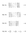
- Eq. (1) shown in Fig. 11A represents a matrix equation which more specifically is a conversion equation for obtaining light emission luminances B 1 ', B 2 ', B 3 ', and B 4 ' from light emission luminances B 01 ', B 02 ', B 03 ', and B 04 ' emitted from light sources 352.
- Eq. (2) shown in Fig. 11B represents a matrix equation which more specifically is a conversion equation for obtaining the light emission luminances B 01 ', B 02 ', B 03 ', and B 04 ' from the light emission luminances B 1 ', B 2 ', B 3 ', and B 4 '.
- Eq. (3) shown in Fig. 11C is obtained by rearranging Eq.
- each light emission luminance B 01 , B 02 , B 03 , and B 04 can be obtained by multiplying each light emission luminance B 1 ', B 2 ', B 3 ', and B 4 ' by coefficients (conversion coefficients) based on amounts of light, emitted from each light source 352 of regions 35a to 35d, which leak out of these region to other regions.
- each of the light emission luminances B 01 , B 02 , B 03 , and B 04 of lights that each of light sources 352 of regions 35a to 35d is expected to emit can be accurately calculated.
- each of the light emission luminances may be approximated by assuming that light emitted from one region leaks to adjacent regions only. That is, the calculation may be performed by zeroing out a term that has k to the power of 2 or greater.
- k 2 times e.g., k n times
- each light emission luminance of light emitted from each region is represented by B 1 ' to B 8 ' respectively, and each light emission luminance of light directly above the corresponding light source 352 is represented by B 1 to B 8 , assuming that each light source 352 emits light individually.
- the light emission luminances B 01 to B 08 can be calculated by Eq. (5) as shown in Fig. 12 .
- light emission luminances B 1 ' to B n ' are obtained by Eq. (6) shown in Fig. 13A
- light emission luminances B 01 to B 0n can be calculated using Eq. (7) shown in Fig. 13B .
- backlight device 35 corresponds to backlight device 35B shown in Fig. 5 .
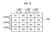
- each leakage light leaked from light source 352 onto regions 35a1 to 35a4, 35b1 to 35b4, 35c1 to 35c4, and 35d1 to 35d4 of backlight device 35B to adjacent regions in the horizontal direction, is assumed to be larger than the light emitted from each of light sources 352 by m times.
- An attenuation coefficient m in the horizontal direction is between 0 and 1.
- the emission of light that leaks to adjacent regions in the vertical direction is k times the light emitted from each of light sources 352 as in the case of backlight device 35A.
- Each light emission luminance for lights that correspond to regions 35a1 to 35a4, 35b1 to 35b4, 35c1 to 35c4, and 35d1 to 35d4 of backlight device 35B that are expected to actually emit is represented by B 11 ' to B 14 ', B 21 ' to B 24 ', B 31 ' to B 34 ', and B 41 ' to B 44 ' respectively.
- each expected light emission luminance of light sources 352 onto their respective regions is represented by B 011 to B 014 , B 021 to B 024 , B 031 to B 034 , and B 041 to B 044 respectively.
- a matrix equation shown in Fig. 15 is obtained.
- Eq. (8) shown in Fig. 15A is a conversion equation given by a matrix equation for obtaining the light emission luminances B 11 ' to B 44 ' from the light emission luminances B 011 to B 044 of lights that light sources 352 emit.
- Eq. (9) shown in Fig. 15B is a conversion equation given by a matrix equation for obtaining the light emission luminances B 011 to B 044 from the light emission luminances B 11 ' to B 44 '.
- Eq. (10) shown in Fig. 15C is obtained.
- each of light emission luminances that the sixty-four regions are expected to emit is represented by B 11 ' to B 88 ' respectively.
- each light emission luminance of light directly above the corresponding light sources 352 is represented by B 011 to B 088 , assuming that each light source 352 emits a light individually.
- the light emission luminances B 11 ' to B 88 ' are obtained by Eq. (12) shown in Fig. 16A
- the light emission luminances B 011 to B 088 can be calculated by Eq. (13) shown in Fig. 16B .
- backlight device 35 is divided into n regions in both the horizontal and vertical directions (n: a positive integer being equal to 2 or greater)and light emission luminances B 011 to B 0n,n can be calculated by Eq. (14) shown in Fig. 17 using light emission luminances B 11 ' to B n,n '.
- nh regions a positive integer being equal to 2 or greater
- nv regions a positive integer being equal to 2 or greater, not being the same value as nh
- the attenuation coefficients k and m for light emission luminance calculator 22 are supplied from controller 50.
- the attenuation coefficients k and m can be varied arbitrarily.
- Data thus obtained which indicate light emission luminances of lights that respective light sources 352 on multiple regions of backlight device 35 emit, are supplied to white balance adjustor 23.
- Temperature data indicative of a temperature of backlight device 35, and color temperature data indicative of a color temperature of a light emitted from backlight device 35 are inputted to white balance adjustor 23.
- the temperature data described above are outputted from temperature sensor 37, while color temperature data described above are outputted from color sensor 38.
- the luminance of a light emitted from an LED changes according to the change of the temperature of backlight device 35. Therefore, when light sources 352 include LEDs of three colors, white balance adjustor 23 adjusts the amount of light of LEDs of R, G, and B based on the temperature data and the color temperature data so that a white balance can be adjusted to optimum.
- the white balance of backlight device 35 can also be adjusted using an external control signal S ct1 supplied from controller 50.
- white balance adjuster 23 can be eliminated.
- Data outputted from white balance adjuster 23 are supplied to PWM timing generator 24.
- the data indicate the luminances of lights from respective sources 352 onto multiple regions of backlight device 35, are supplied to white balance adjustor 23.
- each light source 352 is an LED
- the light emission of an LED of each color is controlled using, for example, a pulse duration modulation signal.
- PWM timing generator 24 supplies backlight driver 36 with PWM timing data, which includes timing for the pulse duration modulation signal, and pulse duration for adjusting the amount of light emission (light emission time).
- Backlight driver 36 generates a drive signal as a pulse duration modulation signal based on the PWM timing data thus inputted, and drives the light sources (LEDs) of backlight device 35.
- each LED is driven by the pulse duration modulation signal.
- a timing generator may be provided that generates timing data for determining when current flows through the LEDs, and the value of the current.
- the light emission may be controlled differently, according to the type of light source, and a timing generator generating timing data according to the kind of light sources may be provided.
- backlight luminance controller 20 and controller 50 are separately provided, all or part of the backlight luminance controller 20 circuits can be provided in controller 50. Further, in the configuration of Fig.
- the maximum gradation detector 11, image gain calculation unit 12, and backlight luminance controller 20 may be configured in hardware, software, or combinations thereof. Without having to repeat the description, i.e., the description on a synchronization in which the displaying of respective frames of image signals on liquid crystal panel 34, the image signals being outputted from image signal processor 10, and the controlling of backlight luminances by backlight luminance controller 20 according to a maximum luminance of image signals are synchronized with each other. In Fig. 1 , the drawing of a configuration on the synchronizing of both described above has been omitted.
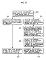
- Step S11 maximum gradation detector 11 detects a maximum gradation of an image signal for each region of liquid crystal panel 34.
- image gain calculator 12 calculates a gain, which is multiplied to image signals for display on respective regions of liquid crystal panel 34.
- Step S13 liquid module unit 30 displays the image signals of the respective regions multiplied by the gain. Steps S14 to S17 are performed in parallel with Steps S12 and S13.
- non-uniformization processor 21 obtains light emission luminances B of lights that are expected from multiple regions of backlight device 35, and multiplies the light emission luminances B by a coefficient p (to be thereafter set as light emission luminances B') so that the luminances of the multiple regions of liquid crystal panel 34 are made non-uniform.
- light emission luminance calculator 22 obtains light emission luminances B 0 of lights to be emitted from light sources 352 themselves on multiple regions of backlight device 35, using a calculation equation using the light emission luminance B' and a conversion coefficient.
- PWM timing generator 24 and backlight driver 36 causes light sources 352 on multiple regions of backlight device 35 to emit as light emission luminance B 0 with synchronization established with Step S13.
- non-uniformization processor 21 obtains light emission luminances B' on which a non-uniformization process is performed
- light emission luminance calculator 22 obtains light emission luminances B 0 based on this light emission luminances B'.
- a non-uniformization process may be performed after obtaining the light emission luminance B 0 using light emission luminance calculator 22. That is, non-uniformization processor 21 and light emission luminance calculator 22 may be interchanged. Such operation and a procedure for this will be described in refer to Fig. 19 .
- Steps S21 to S23 are the same as Steps S11 to S13 of Fig. 18 .
- light emission luminance calculator 22 obtains the light emission luminances B of lights that are expected from multiple regions of backlight device 35, and further, in Step S26, obtains light emission luminances B 0 of lights from light sources 352 themselves on multiple regions of backlight device 35, using a calculation equation that employs light emission luminance B and a conversion coefficient.
- non-uniformization processor 21 multiplies the light emission luminances B 0 by the coefficient p, and sets the result as light emission luminance B 0 '.
- PWM timing generator 24 and backlight driver 36 causes light sources 352 on multiple regions of backlight device 35 to emit light at light emission luminance B 0 ' with synchronization established by Step S23.
- non-uniformization processor 21 a non-uniformization process by non-uniformization processor 21 is necessary when it is desired to further reduce power consumption of backlight device 35 over the configurations described in Non-Patent Document 1 and Patent Documents 1 to 3 described above; however, when the level of required power consumption is the same as that in the configurations of the above-mentioned documents, it is possible to eliminate non-uniformization processor 21. Operation and a representative procedure in this case will be described referring to Fig. 20 . In Fig. 20 , Steps S31 to S33 are the same as Steps S11 to S13 of Fig. 18 .
- Step 34 light emission luminance calculator 22 obtains light emission luminances B of lights which are expected to emit from multiple regions of backlight device 35, and further, in Step S36, obtains light emission luminances B 0 of lights to emit from light sources 352 themselves on multiple regions of the backlight device 35, with a calculation equation using the light emission luminance B and a conversion coefficient. Further, in Step S37, PWM timing generator 24 and backlight driver 36 causes light sources 352 on multiple regions of backlight device 35 to emit light at light emission luminance B 0 with synchronization established via Step S33.
- backlight device 35 has a structure wherein light emitted from respective light sources 352 of multiple regions are allowed to leak to other regions, so that it is not necessary to establish an accurate correspondence between the regions of liquid crystal panel 34 and the regions of backlight device 35. Further, it is possible to accurately obtain the light emission luminances B of lights emitted from the multiple regions of backlight device 35, using the light emission luminances B 0 of light sources 352 themselves in the case where light sources 352 of the respective regions individually emit. Therefore, it is possible to accurately control the luminances of backlights that irradiate multiple regions on liquid crystal panel 34 according to the brightness of image signals to be displayed on these regions.
- the respective regions of liquid crystal panel 34 are not completely independent, and light emission luminances B 0 are obtained by considering the structure in which light emitted from each of light sources 352 leaks to other regions through use of a calculation equation. Therefore, it is possible to enhance the quality of images displayed on liquid crystal panel 34 so that non-uniformities in brightness and color do not tend to occur on multiple regions of liquid crystal panel 34.
- Fig. 21 is a block diagram showing the entire configuration of a liquid crystal display device of a second embodiment.
- the parts that are the same as those shown in Fig. 1 are given the same reference numerals, so that further description thereof is omitted.
- the configuration of Fig. 21 the non-uniformization processor 21 of Fig. 1 has been eliminated, but this may include non-uniformization processor 21 in Fig. 1 as in the first embodiment.
- light emission luminance calculator 22 calculates light emission luminances B 0 of lights from light sources 352 themselves of multiple regions of backlight device 35, and causes each light source 352 of multiple regions to emit light.
- the light emission luminances B 0 each indicate a luminance value at the center of each one of the regions.
- Fig. 22A shows luminance distribution in the case where only region 35b emits light.
- region 35b is one of four regions of backlight device 35A into which backlight device 35 is divided in the vertical direction as in Fig. 4A .
- region 35b emits light at light emission luminance Bo 2 shown in Fig.
- the light emission luminances of regions 35a and 35c each become kBo 2 , and that of region 35d becomes k 2 Bo 2 .
- the amount of light emitting from light source 352 of region 35b can be indicated by the region with hatch lines seen in Fig. 22B . That is, the amount of light shown in Fig. 22B is represented by an integral value of light in a range of the luminance distribution of Fig. 22A .
- Preferably light emission luminances B of lights emitted from multiple regions are obtained using an integral value of light emitted from light source 352, rather than based on light emission luminance Bo of light that emits from light source 352 itself of each region.
- an amount-of-emitted light calculator 25 is provided, which converts light emission luminance Bo into an amount of emitted light Boig as an integral value.
- the amount of emitted light Boig can be easily obtained from a calculation equation, which converts light emission luminance Bo into amount of emitted light Boig.
- Fig. 23A is a calculation equation in the embodiment wherein backlight device 35 is backlight device 35A.
- Fig. 23B shows constants s 1 to s 4 in Eq. (15) shown in Fig. 23A , and expresses these constants s 1 to s 4 by Eq. (16), using an attenuation constant k. Further, the equations shown in Figs. 23A and 23B are approximate and convert a light emission luminance Bo into amount of emitted light Boig. For example, when region 35a of backlight device 35A emits light, an integral value of a light irradiating liquid crystal panel 34 can be approximately expressed by Eq. (17) of Fig.
- Fig. 25A indicates a calculation equation for obtaining an amount of emitted light Boig based on light emission luminance Bo, in the exaqmple of backlight device 35B shown in Figs. 4 and 14 .
- Constants s 1 to s 4 in Eq. (21) shown in Fig. 25A are given by Eq. (16) shown in Fig. 23B
- constants t 1 to t 4 can be expressed by Eq. (22) of Fig. 25B , by using an attenuation coefficient m.
- coefficient s by which light emission luminances Bo of regions located on upper and lower ends are multiplied is represented as equal to 1+k
- coefficient s by which light emission luminances Bo of respective regions sandwiched by those on upper and lower ends are multiplied is equal to (1+k)/(1-k).
- Coefficient t, by which light emission luminances Bo of regions located on left and right ends are multiplied, is equal to 1+m
- coefficient t by which light emission luminances Bo of respective regions sandwiched by those on the left and right ends are multiplied is equal to (1+m)/(1-m).
- Fig. 21 data indicative of the amount of light Boig output from amount-of-emitted light calculator 25 are supplied to PWM timing generator 24 through white balance adjustor 23.
- PWM timing generator 24 generates PWM timing data for adjusting the duration of a pulse duration modulation signal for generation by backlight driver 36, based on data indicative of the amount of emitted light Boig.
- backlight driver 36 drives light sources 352 of respective regions according to emitted light Boig from light sources 352 of the respective regions of backlight device 35, so that it becomes possible to control light emission luminances B of light from multiple regions more adequately than the first embodiment.
- the calculation equations converting the light emission luminances Bo into amounts of emitted light Boig as described using Figs. 23 to 25 are those for approximately obtaining the amount of emitted light Boig as described above, and not for completely representing an integral value of a light corresponding to a region with hatching shown in Fig. 22B . However, even when they are only approximate, it is possible to obtain a value for emitted light Boig that corresponds to the integral value of light. The integral value of a light may be more accurately obtained using a further complicated calculation equation.
- Fig. 26 is a block diagram showing an entire configuration of a liquid crystal display device of a third embodiment.
- the parts which are the same as those shown in Fig. 1 are given the same reference numerals, so that a further description thereof is omitted.
- the non-uniformization processor 21 in Fig. 1 has been eliminated from Fig. 26 , but may include as in the case of the first embodiment.
- the amount-of-emitted light calculator unit 25 has been included in Fig. 26 as in the second embodiment, but also may be eliminated.
- Fig. 27A is a view showing the case where liquid crystal panel 34A is divided into regions 34a to 34d so that regions 34a to 34d correspond to regions 35a to 35d of backlight device 35A respectively.
- This figure also shows the case where the gradations of regions 34a, 34b, and 34d are zero (i.e., black), and the gradation of region 34c is at maximum gradation 255 (i.e., white).
- light emission luminances B of light from regions 35a to 35d of backlight device 35A become B 1 , B 2 , B 3 , and B 4 respectively as shown in Fig. 27B .
- Bo 1 denotes light emission luminances of lights to be emitted from light sources 352 themselves of regions on an upper end
- Bon denotes light emission luminances of lights to be emitted from light sources 352 themselves of regions on a lower end
- Boi denotes light emission luminances of lights to be emitted from light sources 352 themselves of regions sandwiched by the upper and lower ends.
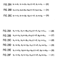
- Bo 1 , Bon, and Boi take negative values due to calculation when light emission luminances B 1 , Bi, and Bn of lights emitted from respective regions fall in the condition indicated by Eq. (23) of Fig. 28A .
- Eq. (23) the condition in which the light emission luminances Bo take negative values depends on the attenuation coefficient k.
- Figs. 29A to 29F show conditions and corrections of light emission luminances B, in which light emission luminances Bo take negative values when the case where backlight device 35 is divided into multiple regions in both the horizontal and vertical directions.
- a subscript, i, of a light emission luminance B denotes an arbitrary i-th region in the vertical direction
- a subscript, j denotes an arbitrary j-th region in the horizontal direction.
- Eq. (26) of Fig. 29A shows a condition for light emission luminances B in which light emission luminances Bo become negative by calculation on respective regions arranged in the vertical direction.
- the light emission luminances B fall in a condition shown in Eq. (26)
- the light emission luminances B are first corrected so as to satisfy Eqs. (27) and (28) of Figs. 29B and 29C , and thereafter the light emission luminances Bo are obtained.
- Eq. (29) of Fig. 29D shows a condition for the light emission luminances B in which the light emission luminances Bo become negative in calculation on respective regions arranged in the horizontal direction.
- the condition in which the light emission luminances Bo become negative in calculation in the case of the horizontal direction is determined depending on the attenuation coefficient m.
- light emission luminances B fall within the condition shown in Eq. (29)
- light emission luminances B are first corrected so as to satisfy Eqs. (30) and (31) of Figs. 29E and 29F , and thereafter the light emission luminances Bo are obtained.
- Fig. 27D shows light emission luminances B, the luminance values of which are corrected so that the light emission luminances Bo of negative values as shown in Fig. 27C do not occur.
- Fig. 27E shows light emission luminances B, the luminance values of which are corrected so that the light emission luminances Bo of negative values as shown in Fig. 27C do not occur.
- image gain calculator 12 obtains a gain using data inputted from maximum gradation detector 11, the data indicating maximum gradations of respective regions of liquid crystal panel 34.
- the third embodiment shown in Fig. 26 is configured as follows. As shown in Figs. 28 and 29 , when the light emission luminances Bo become negative by calculation, light emission luminance calculator 22 corrects the light emission luminances B so that the luminance values of the light emission luminances Bo can be 0 or greater. Thereafter, light emission luminance calculator 22 obtains light emission luminances Bo based on the corrected light emission luminances B, and supplies the same to amount-of-emitted light calculator 25. The light emission luminances B thus corrected are supplied to image gain calculator 12. The image gain calculator 12 calculates a gain by which an image signal is multiplied, based on the corrected light emission luminances B.
- image gain calculator 12 obtains a gain using data indicative of maximum gradations of image signals of respective regions, or even in the case where a gain is obtained using the corrected light emission luminances B, image gain calculator 12 is assumed to obtain a value as a gain for an image signal for each region.
- the value corresponds to that obtained by dividing a maximum gradation that the image signal may take, and wherein the maximum gradation is determined from a bit count of an image signal, by a maximum gradation of an image signal on each region.
- the fourth embodiment maybe configure as described for any one of the above first to third embodiments.
- studies have been made on how luminance distribution characteristics should be treated is preferable, the luminance distribution characteristics being those of lights emitted from light sources 352 of backlight device 35, and this embodiment is configured, to which light sources 352 having preferable luminance distribution characteristics are adopted.
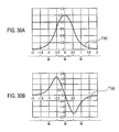
- Fig. 30A is a view showing luminance distribution characteristics of a light emitted from one light source 352 on one region of backlight device 35.
- the light source is assumed to be a point light source.
- the luminance distribution characteristics shown in Fig. 30A correspond to those in the case where a section is viewed, along which respective regions of backlight devices 35A and 35B are each in the vertical direction.
- a vertical axis indicates luminance value
- a horizontal axis indicates distance from light source 352.
- luminance values are indicated in which these are normalized with respect to a maximum luminance value being equal to 1 (central luminance).
- W represents the width of one region in the vertical direction.
- a curve depicted by the luminance distribution characteristics represents a luminance distribution function f(x).
- Fig. 30B shows a derived function f'(x) of the luminance distribution function f(x). From an experimental result, it has been confirmed that a maximum value (a maximum derivative of the luminance distribution function f(x)) of the derived function f'(x) influences visibility of the boundary step.
- the inventors have selectively used, in backlight device 35, a plurality of light sources having fc1 to fc2 being a luminance distribution functions f(x), luminance distribution characteristics of which are different from each other, and studied the visibility of the boundary step.
- fc1 fc2 fc3 fc4 fc5 fc6 fc7 fc8 Maximum derivative 1.2 1.4 1.6 1.8 2.0 2.2 2.5 3.0 Presence of boundary step No No No No No No Yes Yes Yes
- Fig. 31A shows fc1, fc3, fc5, fc7, and fc8;
- Fig. 31B shows derived functions f'c1, f'c3, f'c5, f'c7, and f'c8 of the luminance distribution functions fc1, fc3, fc5, fc7, and fc8.
- Light from light source 352 spreads concentrically with respect to light source 352 as a center with its luminance attenuated with distance from light source 352, so that the same is true also for the case where luminance distribution characteristics of a light from light source 352 are viewed from the horizontal direction or any direction other than the vertical direction.
- the maximum value of the absolute value of the derivative indicating a change in a slope of the luminance distribution function f(x) being represented by the curve of the luminance distribution characteristics is equal to 2.0 or less. Therefore, even when causing only part of a plurality of regions of backlight device 35 to emit light, a boundary of the region is not viewed as a boundary step so that the quality of images to be displayed on liquid crystal panel 34 is not deteriorated.
- Fig. 30 is a view showing the same luminance distribution function f(x) as that of Fig. 30A .
- Fig. 32 when normalizing a central luminance of light source 352 to 1, a light from light source 352 leaks to an adjacent region with the attenuation coefficient k, so that the central luminance of the adjacent region becomes k.
- Fig. 33 is a view showing a relationship between an attenuation coefficient k and a power consumption relative value.
- Img1 and Img2 represent characteristics showing a relationship between attenuation values k and power consumption relative values for still images, pictures of which are different from each other.
- power consumption can be reduced by performing a luminance control of backlight device 35 as described in the first embodiment.
- power consumption does not change much even when the attenuation coefficient k is increased, in the range of attenuation coefficient k being 0.3 or less.
- power consumption comparatively increases with increasing attenuation coefficient k, in the range of attenuation coefficient k exceeding 0.3. Therefore, it can be said that it is preferable that the attenuation coefficient k be 0.3 or less when considering the effect of reduction of power consumption of backlight device 35.
- the attenuation coefficient k in the vertical direction has been described, but the same is true of the case for the attenuation coefficient m in the horizontal direction. That is, when lights emitted from respective light sources of a plurality of regions leak to regions adjacent in the vertical or horizontal direction to own regions, it is preferable that, when a central luminance of the own region is equal to 1, a central luminance of a region adjacent to the own region be greater than 0 and equal to 0.3 or less.
- liquid crystal panel 34 and backlight device 35 of the first to fourth embodiments are assumed to have a plurality of regions of the same area, different areas may be set to the regions when needed. Further, when an image display device which needs a backlight device is newly developed other than liquid crystal display devices, it is possible to naturally apply the present invention to the new image display device.
- the invention includes other embodiments in addition to the above-described embodiments without departing from the spirit of the invention. The embodiments are to be considered in all respects as illustrative, and not restrictive. The scope of the invention is indicated by the appended claims rather than by the foregoing description. Hence, all configurations including the meaning and range within equivalent arrangements of the claims are intended to be embraced in the invention.
Landscapes
- Engineering & Computer Science (AREA)
- Physics & Mathematics (AREA)
- General Physics & Mathematics (AREA)
- Theoretical Computer Science (AREA)
- Computer Hardware Design (AREA)
- Crystallography & Structural Chemistry (AREA)
- Chemical & Material Sciences (AREA)
- Nonlinear Science (AREA)
- Optics & Photonics (AREA)
- Mathematical Physics (AREA)
- Liquid Crystal (AREA)
- Liquid Crystal Display Device Control (AREA)
- Control Of Indicators Other Than Cathode Ray Tubes (AREA)
Applications Claiming Priority (4)
| Application Number | Priority Date | Filing Date | Title |
|---|---|---|---|
| JP2007123136 | 2007-05-08 | ||
| JP2007209819A JP2009042651A (ja) | 2007-08-10 | 2007-08-10 | 液晶表示装置及びこれに用いる映像表示方法 |
| JP2007209820A JP2009042652A (ja) | 2007-08-10 | 2007-08-10 | 液晶表示装置及びこれに用いる映像表示方法 |
| JP2007209818A JP2009042650A (ja) | 2007-08-10 | 2007-08-10 | 液晶表示装置及びこれに用いる映像表示方法 |
Publications (2)
| Publication Number | Publication Date |
|---|---|
| EP1990796A2 true EP1990796A2 (de) | 2008-11-12 |
| EP1990796A3 EP1990796A3 (de) | 2009-07-22 |
Family
ID=39598386
Family Applications (1)
| Application Number | Title | Priority Date | Filing Date |
|---|---|---|---|
| EP08004713A Ceased EP1990796A3 (de) | 2007-05-08 | 2008-03-13 | Flüssigkristallanzeige und Bildanzeigeverfahren dafür |
Country Status (3)
| Country | Link |
|---|---|
| US (1) | US8139020B2 (de) |
| EP (1) | EP1990796A3 (de) |
| KR (1) | KR100885285B1 (de) |
Cited By (7)
| Publication number | Priority date | Publication date | Assignee | Title |
|---|---|---|---|---|
| WO2010020949A1 (en) * | 2008-08-19 | 2010-02-25 | Nxp B.V. | Video processing with spatially-based backlight control |
| EP2113904A3 (de) * | 2008-05-01 | 2010-07-28 | Victor Company Of Japan, Limited | Flüssigkristallanzeige und Bildanzeigeverfahren dafür |
| CN101937653A (zh) * | 2010-09-27 | 2011-01-05 | 彩虹集团公司 | 一种分区亮度一致性调整方法 |
| US8139022B2 (en) | 2007-05-08 | 2012-03-20 | Victor Company Of Japan, Limited | Liquid crystal display device and image display method thereof |
| US8139020B2 (en) | 2007-05-08 | 2012-03-20 | Victor Company Of Japan, Limited | Liquid crystal display device and image display method thereof |
| US8421740B2 (en) | 2008-09-18 | 2013-04-16 | JVC Kenwood Corporation | Liquid crystal display device and image display method thereof |
| US9230489B2 (en) | 2010-07-02 | 2016-01-05 | Semiconductor Energy Laboratory Co., Ltd. | Liquid crystal display device and method for driving liquid crystal display device |
Families Citing this family (55)
| Publication number | Priority date | Publication date | Assignee | Title |
|---|---|---|---|---|
| JP5110355B2 (ja) * | 2007-07-09 | 2012-12-26 | Nltテクノロジー株式会社 | 液晶表示装置のバックライト駆動方法及びその装置並びに液晶表示装置 |
| JP4806102B2 (ja) * | 2008-06-27 | 2011-11-02 | シャープ株式会社 | 液晶表示装置の制御装置、液晶表示装置、液晶表示装置の制御方法、プログラムおよび記録媒体 |
| KR101520783B1 (ko) * | 2008-09-08 | 2015-05-18 | 삼성디스플레이 주식회사 | 표시 장치의 구동 방법, 이를 수행하기 위한 표시 장치 및 타이밍 컨트롤러 |
| KR101521098B1 (ko) * | 2009-01-06 | 2015-05-20 | 삼성디스플레이 주식회사 | 광원 구동 방법 및 이를 수행하기 위한 광원 장치 |
| CN102292759B (zh) | 2009-02-16 | 2014-09-24 | 夏普株式会社 | 照明装置、显示装置、数据生成方法、数据生成程序和记录介质 |
| KR101605157B1 (ko) * | 2009-03-24 | 2016-03-22 | 삼성디스플레이 주식회사 | 표시 장치 구동 방법 |
| CN101848574A (zh) * | 2009-03-27 | 2010-09-29 | 北京京东方光电科技有限公司 | 发光二极管背光源的驱动装置和亮度调整方法 |
| KR101612455B1 (ko) * | 2009-04-16 | 2016-04-15 | 삼성디스플레이 주식회사 | 화소 데이터의 보정 방법 및 이를 수행하기 위한 표시 장치 |
| EP2433274A1 (de) * | 2009-05-20 | 2012-03-28 | Marvell World Trade Ltd. | Flüssigkristallanzeige-hintergrundbeleuchtungssteuerung |
| WO2010137436A1 (ja) | 2009-05-27 | 2010-12-02 | ローム株式会社 | 照明装置 |
| JP2012529081A (ja) * | 2009-06-03 | 2012-11-15 | マニュファクチャリング・リソーシズ・インターナショナル・インコーポレーテッド | Ledバックライトの動的減光 |
| JP5516586B2 (ja) | 2009-07-23 | 2014-06-11 | 富士通株式会社 | 表示装置 |
| JPWO2011013404A1 (ja) * | 2009-07-29 | 2013-01-07 | シャープ株式会社 | 画像表示装置および画像表示方法 |
| BR112012001784A2 (pt) * | 2009-07-30 | 2019-09-24 | Sharp Kk | "dispositivo de exibição de imagem e método de exibição de imagem" |
| JP4693919B2 (ja) * | 2009-09-10 | 2011-06-01 | 株式会社東芝 | 映像表示装置及び映像表示方法 |
| KR101318444B1 (ko) * | 2009-11-23 | 2013-10-16 | 엘지디스플레이 주식회사 | 픽셀 데이터 보상 방법과 이를 이용한 액정표시장치 |
| KR101341016B1 (ko) | 2009-12-11 | 2014-01-07 | 엘지디스플레이 주식회사 | 액정 표시 장치의 로컬 디밍 구동 방법 및 장치 |
| KR101675840B1 (ko) * | 2009-12-14 | 2016-11-14 | 엘지디스플레이 주식회사 | 액정 표시 장치의 로컬 디밍 구동 방법 및 장치 |
| US9324279B2 (en) * | 2010-02-24 | 2016-04-26 | Sharp Kabushiki Kaisha | Illumination device, display device, data generation method, non-transitory computer readable recording medium including data generation program for generating light amount adjustment data based on temperature |
| EP2515291B1 (de) * | 2010-02-24 | 2016-11-02 | Sharp Kabushiki Kaisha | Lichtemittierende vorrichtung für eine bildanzeige |
| JP5650422B2 (ja) * | 2010-03-24 | 2015-01-07 | ソニー株式会社 | 液晶表示装置 |
| JP5460435B2 (ja) | 2010-04-09 | 2014-04-02 | 日立コンシューマエレクトロニクス株式会社 | 画像表示装置および画像表示装置の制御方法 |
| JP5541546B2 (ja) | 2010-04-23 | 2014-07-09 | Necディスプレイソリューションズ株式会社 | 表示装置、表示方法およびプログラム |
| JP5661336B2 (ja) | 2010-05-28 | 2015-01-28 | 日立マクセル株式会社 | 液晶表示装置 |
| US20110304597A1 (en) * | 2010-06-09 | 2011-12-15 | Apple Inc. | Low power backlight for display |
| CN102347322B (zh) * | 2010-08-02 | 2013-07-10 | 晶元光电股份有限公司 | 发光元件、背光模块装置和照明装置 |
| JP5197697B2 (ja) * | 2010-09-06 | 2013-05-15 | 株式会社東芝 | 映像表示装置および情報処理装置 |
| CN101976549B (zh) * | 2010-11-17 | 2012-06-27 | 福州大学 | 一种拼接式大面积场致发射背光源的动态调光电路 |
| JP5932381B2 (ja) * | 2011-04-12 | 2016-06-08 | キヤノン株式会社 | 画像表示装置及びその制御方法 |
| WO2012147651A1 (ja) | 2011-04-27 | 2012-11-01 | シャープ株式会社 | マルチディスプレイ装置及び画像表示装置 |
| US9208730B2 (en) * | 2011-05-13 | 2015-12-08 | Samsung Display Co., Ltd. | Optimization of light source drive values in backlight systems |
| US8982038B2 (en) * | 2011-05-13 | 2015-03-17 | Samsung Display Co., Ltd. | Local dimming display architecture which accommodates irregular backlights |
| US8963895B2 (en) | 2011-09-22 | 2015-02-24 | Nano Lumens Acquisition Inc. | Ubiquitously mountable image display system |
| JP2013104912A (ja) | 2011-11-10 | 2013-05-30 | Sony Corp | 表示装置および表示方法 |
| KR101354333B1 (ko) | 2012-02-24 | 2014-01-27 | 엘지디스플레이 주식회사 | 백라이트 디밍 방법과 이를 이용한 액정표시장치 |
| CN103366693A (zh) * | 2012-04-06 | 2013-10-23 | 联咏科技股份有限公司 | 亮度补偿方法及其区域调光电路与液晶显示器 |
| KR102060604B1 (ko) | 2013-02-28 | 2019-12-31 | 삼성디스플레이 주식회사 | 휘도 조절부, 이를 포함하는 표시 장치 및 이를 이용한 휘도 조절 방법 |
| CN103400554B (zh) * | 2013-08-12 | 2015-07-08 | 合肥工业大学 | 一种led分区背光光扩散函数模板的测试方法 |
| US10319408B2 (en) | 2015-03-30 | 2019-06-11 | Manufacturing Resources International, Inc. | Monolithic display with separately controllable sections |
| US10922736B2 (en) | 2015-05-15 | 2021-02-16 | Manufacturing Resources International, Inc. | Smart electronic display for restaurants |
| US10269156B2 (en) | 2015-06-05 | 2019-04-23 | Manufacturing Resources International, Inc. | System and method for blending order confirmation over menu board background |
| US9924604B2 (en) | 2015-11-04 | 2018-03-20 | Nanolumens Acquisition, Inc. | Modular flexible convex display system and methods |
| TWI569062B (zh) * | 2016-03-08 | 2017-02-01 | 友達光電股份有限公司 | 顯示裝置、顯示裝置的操作方法、及顯示裝置的像素電路 |
| US10319271B2 (en) | 2016-03-22 | 2019-06-11 | Manufacturing Resources International, Inc. | Cyclic redundancy check for electronic displays |
| US10313037B2 (en) | 2016-05-31 | 2019-06-04 | Manufacturing Resources International, Inc. | Electronic display remote image verification system and method |
| WO2018031717A2 (en) | 2016-08-10 | 2018-02-15 | Manufacturing Resources International, Inc. | Dynamic dimming led backlight for lcd array |
| US10770008B2 (en) * | 2017-07-31 | 2020-09-08 | Japan Display Inc. | Display device with dimming panel |
| CN111883070B (zh) * | 2020-07-30 | 2021-09-10 | 重庆惠科金渝光电科技有限公司 | 一种显示面板的驱动方法、驱动模块和显示装置 |
| JP2022131262A (ja) | 2021-02-26 | 2022-09-07 | 日亜化学工業株式会社 | 画像表示方法及び画像表示装置 |
| KR20230031422A (ko) * | 2021-08-27 | 2023-03-07 | 삼성전자주식회사 | 디스플레이 장치 및 그 제어 방법 |
| US11895362B2 (en) | 2021-10-29 | 2024-02-06 | Manufacturing Resources International, Inc. | Proof of play for images displayed at electronic displays |
| CN114677958B (zh) * | 2022-03-30 | 2023-12-15 | 卡莱特云科技股份有限公司 | 一种led显示屏的校正方法、装置及系统 |
| JP2024086278A (ja) * | 2022-12-16 | 2024-06-27 | 日亜化学工業株式会社 | 画像表示装置及び画像表示方法 |
| US12361900B2 (en) * | 2023-11-07 | 2025-07-15 | Synaptics Incorporated | Local dimming for panel display devices using one-dimensional (1D) light source array |
| JP2026023892A (ja) * | 2024-08-01 | 2026-02-13 | 株式会社ジャパンディスプレイ | 表示装置 |
Family Cites Families (30)
| Publication number | Priority date | Publication date | Assignee | Title |
|---|---|---|---|---|
| JPH06102484A (ja) * | 1992-09-18 | 1994-04-15 | Matsushita Electric Ind Co Ltd | 空間光変調素子を用いた映像表示方法及び映像表示装置 |
| US20020096479A1 (en) * | 2000-06-02 | 2002-07-25 | Butters Brian E. | System and method for photocatalytic treatment of contaminated media |
| JPH11109317A (ja) | 1997-09-30 | 1999-04-23 | Sony Corp | 液晶表示装置 |
| JP4574057B2 (ja) * | 2000-05-08 | 2010-11-04 | キヤノン株式会社 | 表示装置 |
| JP3523170B2 (ja) | 2000-09-21 | 2004-04-26 | 株式会社東芝 | 表示装置 |
| KR100415510B1 (ko) * | 2001-03-15 | 2004-01-16 | 삼성전자주식회사 | 적응형 휘도 증대 기능을 갖는 액정 표시 장치 및 이의구동 방법 |
| JP3850241B2 (ja) * | 2001-07-19 | 2006-11-29 | シャープ株式会社 | 照明装置およびそれを用いた液晶表示装置 |
| CN100358001C (zh) | 2002-03-07 | 2007-12-26 | 夏普株式会社 | 显示装置 |
| US7271790B2 (en) * | 2002-10-11 | 2007-09-18 | Elcos Microdisplay Technology, Inc. | Combined temperature and color-temperature control and compensation method for microdisplay systems |
| US7656371B2 (en) | 2003-07-28 | 2010-02-02 | Nichia Corporation | Light emitting apparatus, LED lighting, LED light emitting apparatus, and control method of light emitting apparatus |
| KR100989159B1 (ko) * | 2003-12-29 | 2010-10-20 | 엘지디스플레이 주식회사 | 액정표시장치와 그 제어방법 |
| JP4628770B2 (ja) | 2004-02-09 | 2011-02-09 | 株式会社日立製作所 | 照明装置を備えた画像表示装置及び画像表示方法 |
| TWI239213B (en) | 2004-06-04 | 2005-09-01 | Prodisc Technology Inc | Display device |
| JP4689204B2 (ja) | 2004-07-16 | 2011-05-25 | シャープ株式会社 | 画像表示装置 |
| JP2006047594A (ja) | 2004-08-03 | 2006-02-16 | Funai Electric Co Ltd | 液晶表示装置 |
| JP4529585B2 (ja) | 2004-08-18 | 2010-08-25 | ソニー株式会社 | 表示装置及びその制御装置 |
| JP2006113311A (ja) | 2004-10-15 | 2006-04-27 | Hitachi Displays Ltd | 表示装置 |
| JP2006145886A (ja) | 2004-11-19 | 2006-06-08 | Sony Corp | 表示装置及びその制御方法 |
| JP4904783B2 (ja) | 2005-03-24 | 2012-03-28 | ソニー株式会社 | 表示装置及び表示方法 |
| CN100474388C (zh) | 2005-03-24 | 2009-04-01 | 索尼株式会社 | 显示装置和显示方法 |
| TWI330270B (en) * | 2005-03-29 | 2010-09-11 | Chi Mei Optoelectronics Corp | Region-based displayer and display method thereof |
| JP2006276677A (ja) * | 2005-03-30 | 2006-10-12 | Toshiba Corp | 表示装置と表示装置の駆動方法 |
| KR101169051B1 (ko) * | 2005-06-30 | 2012-07-26 | 엘지디스플레이 주식회사 | 액정 표시 장치 및 그의 구동 방법 |
| JP4602184B2 (ja) * | 2005-07-27 | 2010-12-22 | 株式会社東芝 | 映像表示処理装置とそのバックライト制御方法 |
| JP4621558B2 (ja) * | 2005-07-27 | 2011-01-26 | 株式会社東芝 | 映像表示処理装置とそのバックライト制御方法 |
| JP4991212B2 (ja) * | 2005-10-13 | 2012-08-01 | ルネサスエレクトロニクス株式会社 | 表示駆動回路 |
| JP4237220B2 (ja) * | 2006-11-13 | 2009-03-11 | シャープ株式会社 | 透過型ディスプレイ装置 |
| KR100855472B1 (ko) | 2007-02-07 | 2008-09-01 | 삼성전자주식회사 | 저전력 구동 장치 및 방법 |
| JP2008203292A (ja) | 2007-02-16 | 2008-09-04 | Seiko Epson Corp | 画像表示装置、及び画像表示方法 |
| KR100885285B1 (ko) | 2007-05-08 | 2009-02-23 | 닛뽕빅터 가부시키가이샤 | 액정 표시 장치 및 이에 이용되는 영상 표시 방법 |
-
2007
- 2007-11-14 KR KR1020070116160A patent/KR100885285B1/ko active Active
-
2008
- 2008-03-12 US US12/046,687 patent/US8139020B2/en active Active
- 2008-03-13 EP EP08004713A patent/EP1990796A3/de not_active Ceased
Non-Patent Citations (1)
| Title |
|---|
| None |
Cited By (7)
| Publication number | Priority date | Publication date | Assignee | Title |
|---|---|---|---|---|
| US8139022B2 (en) | 2007-05-08 | 2012-03-20 | Victor Company Of Japan, Limited | Liquid crystal display device and image display method thereof |
| US8139020B2 (en) | 2007-05-08 | 2012-03-20 | Victor Company Of Japan, Limited | Liquid crystal display device and image display method thereof |
| EP2113904A3 (de) * | 2008-05-01 | 2010-07-28 | Victor Company Of Japan, Limited | Flüssigkristallanzeige und Bildanzeigeverfahren dafür |
| WO2010020949A1 (en) * | 2008-08-19 | 2010-02-25 | Nxp B.V. | Video processing with spatially-based backlight control |
| US8421740B2 (en) | 2008-09-18 | 2013-04-16 | JVC Kenwood Corporation | Liquid crystal display device and image display method thereof |
| US9230489B2 (en) | 2010-07-02 | 2016-01-05 | Semiconductor Energy Laboratory Co., Ltd. | Liquid crystal display device and method for driving liquid crystal display device |
| CN101937653A (zh) * | 2010-09-27 | 2011-01-05 | 彩虹集团公司 | 一种分区亮度一致性调整方法 |
Also Published As
| Publication number | Publication date |
|---|---|
| KR100885285B1 (ko) | 2009-02-23 |
| KR20080099116A (ko) | 2008-11-12 |
| US20080278432A1 (en) | 2008-11-13 |
| US8139020B2 (en) | 2012-03-20 |
| EP1990796A3 (de) | 2009-07-22 |
Similar Documents
| Publication | Publication Date | Title |
|---|---|---|
| US8139020B2 (en) | Liquid crystal display device and image display method thereof | |
| US8139022B2 (en) | Liquid crystal display device and image display method thereof | |
| EP2166532B1 (de) | Flüssigkristallanzeige und zugehöriges Bildanzeigeverfahren | |
| EP2154673A2 (de) | Flüssigkristallanzeige und Bildanzeigeverfahren dafür | |
| EP2113904A2 (de) | Flüssigkristallanzeige und Bildanzeigeverfahren dafür | |
| KR101351414B1 (ko) | 액정 표시 장치의 로컬 디밍 구동 방법 및 장치 | |
| JP2008304908A (ja) | 液晶表示装置及びこれに用いる映像表示方法 | |
| TWI421846B (zh) | 分析光源之光分佈的方法及使用該方法驅動液晶顯示裝置之區域調光的方法與裝置 | |
| KR101097584B1 (ko) | 액정표시장치의 휘도제어 장치 및 방법 | |
| JP5070331B2 (ja) | 照明装置およびこれを備えた表示装置 | |
| KR101295882B1 (ko) | 액정표시장치 및 그의 로컬디밍 제어방법 | |
| US9324279B2 (en) | Illumination device, display device, data generation method, non-transitory computer readable recording medium including data generation program for generating light amount adjustment data based on temperature | |
| JP2009042652A (ja) | 液晶表示装置及びこれに用いる映像表示方法 | |
| US20120206502A1 (en) | Method of Driving a Display Panel and Display Apparatus for Performing the Same | |
| KR20110070233A (ko) | 백라이트 유닛과 그를 이용한 액정 표시 장치의 로컬 디밍 구동 방법 및 장치 | |
| JP2009042650A (ja) | 液晶表示装置及びこれに用いる映像表示方法 | |
| JP2009042651A (ja) | 液晶表示装置及びこれに用いる映像表示方法 | |
| JP2009540354A (ja) | 表示デバイス及びその照明方法 | |
| JP5176896B2 (ja) | 液晶表示装置 | |
| KR101768668B1 (ko) | 액정 표시 장치의 구동 방법 | |
| KR101975494B1 (ko) | 액정 표시 장치의 로컬 디밍 장치 및 로컬 디밍 방법, 이를 이용한 액정 표시 장치의 구동 장치 및 구동 방법 | |
| JP2011033985A (ja) | 液晶表示装置及びこれに用いる映像表示方法 |
Legal Events
| Date | Code | Title | Description |
|---|---|---|---|
| PUAI | Public reference made under article 153(3) epc to a published international application that has entered the european phase |
Free format text: ORIGINAL CODE: 0009012 |
|
| AK | Designated contracting states |
Kind code of ref document: A2 Designated state(s): AT BE BG CH CY CZ DE DK EE ES FI FR GB GR HR HU IE IS IT LI LT LU LV MC MT NL NO PL PT RO SE SI SK TR |
|
| AX | Request for extension of the european patent |
Extension state: AL BA MK RS |
|
| PUAL | Search report despatched |
Free format text: ORIGINAL CODE: 0009013 |
|
| AK | Designated contracting states |
Kind code of ref document: A3 Designated state(s): AT BE BG CH CY CZ DE DK EE ES FI FR GB GR HR HU IE IS IT LI LT LU LV MC MT NL NO PL PT RO SE SI SK TR |
|
| AX | Request for extension of the european patent |
Extension state: AL BA MK RS |
|
| 17P | Request for examination filed |
Effective date: 20091223 |
|
| 17Q | First examination report despatched |
Effective date: 20100129 |
|
| AKX | Designation fees paid |
Designated state(s): DE FR GB |
|
| RAP1 | Party data changed (applicant data changed or rights of an application transferred) |
Owner name: JVC KENWOOD CORPORATION |
|
| STAA | Information on the status of an ep patent application or granted ep patent |
Free format text: STATUS: THE APPLICATION HAS BEEN REFUSED |
|
| 18R | Application refused |
Effective date: 20130718 |