EP1990823B1 - Plasmaanzeigevorrichtung - Google Patents
Plasmaanzeigevorrichtung Download PDFInfo
- Publication number
- EP1990823B1 EP1990823B1 EP07714957A EP07714957A EP1990823B1 EP 1990823 B1 EP1990823 B1 EP 1990823B1 EP 07714957 A EP07714957 A EP 07714957A EP 07714957 A EP07714957 A EP 07714957A EP 1990823 B1 EP1990823 B1 EP 1990823B1
- Authority
- EP
- European Patent Office
- Prior art keywords
- plasma display
- main electrode
- electrodes
- electrode
- data
- Prior art date
- Legal status (The legal status is an assumption and is not a legal conclusion. Google has not performed a legal analysis and makes no representation as to the accuracy of the status listed.)
- Not-in-force
Links
- 239000000758 substrate Substances 0.000 claims abstract description 22
- 230000002093 peripheral effect Effects 0.000 claims description 14
- 230000007704 transition Effects 0.000 claims description 5
- 239000010410 layer Substances 0.000 description 29
- OAICVXFJPJFONN-UHFFFAOYSA-N Phosphorus Chemical compound [P] OAICVXFJPJFONN-UHFFFAOYSA-N 0.000 description 18
- 230000004888 barrier function Effects 0.000 description 12
- 239000011521 glass Substances 0.000 description 7
- 230000015556 catabolic process Effects 0.000 description 6
- 230000003247 decreasing effect Effects 0.000 description 4
- 238000010586 diagram Methods 0.000 description 4
- 239000000463 material Substances 0.000 description 4
- 230000032683 aging Effects 0.000 description 3
- 238000000034 method Methods 0.000 description 3
- 239000011241 protective layer Substances 0.000 description 3
- BQCADISMDOOEFD-UHFFFAOYSA-N Silver Chemical compound [Ag] BQCADISMDOOEFD-UHFFFAOYSA-N 0.000 description 2
- 239000004020 conductor Substances 0.000 description 2
- 230000007423 decrease Effects 0.000 description 2
- CPLXHLVBOLITMK-UHFFFAOYSA-N magnesium oxide Inorganic materials [Mg]=O CPLXHLVBOLITMK-UHFFFAOYSA-N 0.000 description 2
- 239000000395 magnesium oxide Substances 0.000 description 2
- AXZKOIWUVFPNLO-UHFFFAOYSA-N magnesium;oxygen(2-) Chemical compound [O-2].[Mg+2] AXZKOIWUVFPNLO-UHFFFAOYSA-N 0.000 description 2
- 238000004519 manufacturing process Methods 0.000 description 2
- 239000003566 sealing material Substances 0.000 description 2
- 229910052709 silver Inorganic materials 0.000 description 2
- 239000004332 silver Substances 0.000 description 2
- 229910052782 aluminium Inorganic materials 0.000 description 1
- XAGFODPZIPBFFR-UHFFFAOYSA-N aluminium Chemical compound [Al] XAGFODPZIPBFFR-UHFFFAOYSA-N 0.000 description 1
- 230000000694 effects Effects 0.000 description 1
- 230000005684 electric field Effects 0.000 description 1
- AMGQUBHHOARCQH-UHFFFAOYSA-N indium;oxotin Chemical compound [In].[Sn]=O AMGQUBHHOARCQH-UHFFFAOYSA-N 0.000 description 1
- 239000004973 liquid crystal related substance Substances 0.000 description 1
- 229910052751 metal Inorganic materials 0.000 description 1
- 239000002184 metal Substances 0.000 description 1
- 229910052754 neon Inorganic materials 0.000 description 1
- GKAOGPIIYCISHV-UHFFFAOYSA-N neon atom Chemical compound [Ne] GKAOGPIIYCISHV-UHFFFAOYSA-N 0.000 description 1
- 238000005192 partition Methods 0.000 description 1
- 239000004065 semiconductor Substances 0.000 description 1
- 238000000638 solvent extraction Methods 0.000 description 1
- 229910052724 xenon Inorganic materials 0.000 description 1
- FHNFHKCVQCLJFQ-UHFFFAOYSA-N xenon atom Chemical compound [Xe] FHNFHKCVQCLJFQ-UHFFFAOYSA-N 0.000 description 1
Images


Classifications
-
- H—ELECTRICITY
- H01—ELECTRIC ELEMENTS
- H01J—ELECTRIC DISCHARGE TUBES OR DISCHARGE LAMPS
- H01J11/00—Gas-filled discharge tubes with alternating current induction of the discharge, e.g. alternating current plasma display panels [AC-PDP]; Gas-filled discharge tubes without any main electrode inside the vessel; Gas-filled discharge tubes with at least one main electrode outside the vessel
- H01J11/20—Constructional details
- H01J11/22—Electrodes, e.g. special shape, material or configuration
- H01J11/26—Address electrodes
-
- H—ELECTRICITY
- H01—ELECTRIC ELEMENTS
- H01J—ELECTRIC DISCHARGE TUBES OR DISCHARGE LAMPS
- H01J11/00—Gas-filled discharge tubes with alternating current induction of the discharge, e.g. alternating current plasma display panels [AC-PDP]; Gas-filled discharge tubes without any main electrode inside the vessel; Gas-filled discharge tubes with at least one main electrode outside the vessel
- H01J11/10—AC-PDPs with at least one main electrode being out of contact with the plasma
- H01J11/12—AC-PDPs with at least one main electrode being out of contact with the plasma with main electrodes provided on both sides of the discharge space
-
- H—ELECTRICITY
- H01—ELECTRIC ELEMENTS
- H01J—ELECTRIC DISCHARGE TUBES OR DISCHARGE LAMPS
- H01J2211/00—Plasma display panels with alternate current induction of the discharge, e.g. AC-PDPs
- H01J2211/20—Constructional details
- H01J2211/22—Electrodes
- H01J2211/26—Address electrodes
- H01J2211/265—Shape, e.g. cross section or pattern
-
- H—ELECTRICITY
- H01—ELECTRIC ELEMENTS
- H01J—ELECTRIC DISCHARGE TUBES OR DISCHARGE LAMPS
- H01J2211/00—Plasma display panels with alternate current induction of the discharge, e.g. AC-PDPs
- H01J2211/20—Constructional details
- H01J2211/22—Electrodes
- H01J2211/32—Disposition of the electrodes
- H01J2211/323—Mutual disposition of electrodes
Definitions
- the present invention relates to a plasma display device in which a plasma display panel is used as a display device.
- the plasma display panels (hereinafter also referred to as "panel") conventionally for use in a plasma display device are roughly classified into an AC type and a DC type having different driving methods.
- the panels also fall into two types having different discharge systems: a surface discharge type and an opposite discharge type.
- the current mainstream of the panels is the surface discharge type having a three-electrode structure because this type has higher definition, a larger screen, and simpler manufacturing method.
- a surface discharge plasma display panel is structured so that a pair of substrates having a transparent one at least on the front side thereof is faced to each other to form a discharge space therebetween. Further, barrier ribs for partitioning the discharge space into a plurality of spaces are formed on the substrates. Electrode groups are formed on each of the substrates so that discharge occurs in the discharge space partitioned by the barrier ribs. Further, phosphor layers that emit red, green, or blue light are provided in the discharge space. Thus, a plurality of discharge cells is formed. The phosphors are excited by vacuum ultraviolet light that has a short wavelength and is generated by the discharge. Then, the discharge cells having phosphors for emitting red, green, and blue light (red discharge cells, green discharge cells, and blue discharge cells) generate red, green, and blue visible light, respectively. Thus, color display is provided in the panel.
- Such a plasma display panel can provide faster display and a larger viewing angle than a liquid crystal panel.
- the screen size thereof can be increased more easily.
- the plasma display panel is the self-luminous type, and thus has high display quality. For these reasons, recently, the plasma display panel has been drawing attention particularly among flat panel displays and finding a wide rage of applications, as a display device in a place many people gather or a display device with which people enjoy images on a large screen at home.
- a panel is held on the front side of a chassis member, and a circuit board is disposed on the rear side of the chassis member.
- a module is formed.
- the panel is predominantly made of glass, and the chassis member is made of a metal, such as aluminum.
- the circuit board constitutes a driver circuit for causing the panel to emit light.
- Patent application US 2005/0052137 A discloses a plasma display device including a plasma display panel and a data driver.
- the plasma display panel includes a front substrate and a rear substrate faced to each other to form a discharge space therebetween.
- the front substrate includes a plurality of display electrodes.
- the rear substrate includes a plurality of data electrodes intersected with the display electrodes. Discharges cells are formed at the intersections of the display electrodes and data electrodes.
- the data driver is coupled to the data electrodes to supply voltage to the data electrodes.
- each of the data electrodes has a plurality of main electrode parts provided at the portions facing the display electrodes at the discharge cells, and wiring parts that connect the plurality of main electrode parts together and have a width smaller than the widths of the main electrode parts.
- the widths of the main electrode parts provided in a peripheral portion of the plasma display panel are larger than the widths of the main electrode parts provided in a central portion thereof.
- the present invention as defined in claim 1 provides a plasma display device having higher image quality and lower power consumption.
- FIG. 1 a description of a structure of a plasma display panel for use in the plasma display device is provided, with reference to Fig. 1 .
- plasma display panel 11 (hereinafter referred to as panel 11) is structured so that front panel 31 and rear panel 32 are faced to each other to form discharge space 60 therebetween.
- Front panel 31 and rear panel 32 are sealed with a sealing material (not shown) provided along the peripheries of the panels.
- the examples of the sealing material include a glass frit.
- a mixed gas of neon (Ne) and xenon (Xe), for example, is filled into discharge space 60.
- Front panel 31 is structured in the following manner.
- Display electrodes 62 each made of scan electrode 3 and sustain electrode 4, are disposed in a plurality of rows, on front substrate 1 made of glass. Sustain electrodes 3 and sustain electrodes 4 constituting display electrodes 62 are disposed in parallel with each other via discharge gaps 64.
- Dielectric layer 5 made of a glass material is formed to cover scan electrodes 3 and sustain electrodes 4.
- protective layer 6 made of magnesium oxide (MgO) is formed on dielectric layer 5.
- front panel 31 is formed.
- each scan electrode 3 has transparent electrode 3a, and bus electrode 3b formed on transparent electrode 3a.
- each sustain electrode 4 has transparent electrode 4a, and bus electrode 4b formed on transparent electrode 4a.
- Transparent electrodes 3a and 4a are made of indium tin oxide (ITO) or other materials, and are optically transparent.
- Bus electrodes 3b and 4b are predominantly made of a conductive material, such as silver (Ag).
- Rear panel 32 is structured in the following manner.
- a plurality of data electrodes 8 made of a conductive material, such as silver (Ag), are disposed in a stripe pattern on glass rear substrate 2 faced to front substrate 1.
- Data electrodes 8 are covered with insulating layer 7 made of a glass material.
- barrier ribs 9 are formed on insulating layer 7 to partition discharge space 60 for each discharge cell 61.
- phosphor layers 10 of red (R), green (G), or blue (B) are provided over the surface of insulating layer 7 between barrier ribs 9 and the side faces of barrier ribs 9. In this manner, rear panel 32 is formed.
- Front substrate 1 and rear substrate 2 are faced to each other so that data electrodes 8 are intersected with scan electrodes 3 and sustain electrodes 4.
- discharge cells 61 partitioned by barrier ribs 9 are formed at the intersections between scan electrodes 3 and sustain electrodes 4, and data electrodes 8.
- black light-block layer 33 having high light-blocking effect may be provided between display electrodes 62 and adjacent display electrodes 62 to improve the contrast.
- panel 11 is not limited to the above.
- panel 11 may be structured to have barrier ribs 9 in a stripe pattern.
- Fig. 1 shows a structure of display electrodes 62 in which scan electrodes 3 and sustain electrodes 4 are alternately disposed in the following order: scan electrode 3 - sustain electrode 4 - scan electrode 3 - sustain electrode 4, and so on.
- display electrodes 62 may be an array of electrodes in the following order: scan electrode 3 - sustain electrode 4 - sustain electrode 4 - scan electrode 3, and so on.
- Fig. 2 is a schematic electrode array diagram of plasma display panel 11 of Fig. 1 .
- N scan electrodes SC 1 to SCn, i.e. scan electrodes 3, and n sustain electrodes SU 1 to SUn, i.e. sustain electrodes 4, are disposed in the row (vertical) direction.
- m data electrodes D1 to Dm, i.e. data electrodes 8 are disposed in the column (horizontal) direction.
- m x n discharge cells 61 are formed in discharge space 60.
- These m x n discharge cells 61 form a display area in which images are displayed.
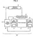
- Fig. 3 is a circuit block diagram of a plasma display device in which plasma display panel 11 is used.
- Plasma display device 63 includes panel 11, and various electrical circuits for driving panel 11.
- the various electrical circuits include image signal processing circuit 12, data electrode driver circuit 13, scan electrode driver circuit 14, sustain electrode driver circuit 15, timing generating circuit 16, and power supply circuits (not shown).
- data electrode driver circuit 13 is coupled to one ends of data electrodes 8.
- Data electrode driver circuit 13 includes a plurality of data drivers 13a for supplying voltage to data electrodes 8 and made of semiconductor devices.
- Data electrodes 8 are divided into a plurality of blocks so that one block has a plurality of data electrodes 8. Each block has one data driver 13a.
- Data driver 13a is coupled to an electrode lead part that is led out from data electrodes 8 at bottom end 11a of panel 11.
- timing generating circuit 16 generates various kinds of timing signals based on horizontal synchronizing signal H and vertical synchronizing signal V, and feeds the timing signals to the respective driver circuit blocks, i.e. image signal processing circuit 12, data electrode driver circuit 13, scan electrode driver circuit 14, and sustain electrode driver circuit 15.
- Image signal processing circuit 12 converts image signal Sig into image data for each sub-field.
- Data electrode driver circuit 13 converts the image data for each sub-field into signals corresponding to respective data electrodes D1 to Dm. By using the signals converted by data electrode driver circuit 13, respective data electrodes D1 to Dm are driven.
- Scan electrode driver circuit 14 supplies a driving voltage waveform to scan electrodes SC1 to SCn based on the timing signals supplied from timing generating circuit 16.
- sustain electrode driver circuit 15 supplies a driving voltage waveform to sustain electrodes SU1 to SUn based on the timing signals supplied from timing generating circuit 16.
- Each of scan electrode driver circuit 14 and sustain electrode driver circuit 15 has sustain pulse generating circuit 17 therein.
- Fig. 4 is a waveform chart showing the driving voltage waveforms to be applied to the respective electrodes of panel 11.
- one field period is divided into a plurality of sub-fields, and each sub-field has a initializing period, an address period, and a sustain period.
- sustain electrodes SU1 to SUn are kept at positive voltage Vh (V).
- Applied to scan electrodes SC1 to SCn is ramp voltage Vi34 gradually decreasing from voltage Vi3 (V) to voltage Vi4 (V).
- This application causes the second weak initializing discharge in all discharge cells 61, and weakens the wall voltage on scan electrodes SC1 to SCn and sustain electrodes SU1 to SUn. Further, the wall voltage on data electrodes D1 to Dm is adjusted to a value appropriate for addressing operation.
- the addressing operation is performed so that addressing discharge occurs in discharge cells 61 to be lit in the first row, and wall voltage is accumulated on the corresponding electrodes.
- the voltage at the intersections between data electrodes D1 to Dm to which no address pulse voltage Vd (V) is applied and scan electrode SC1 does not exceed the breakdown voltage, thus causing no addressing discharge.
- the addressing operation is sequentially performed on discharge cells 61 in the second row to n-th row. Thus, the address period in the first sub-field is completed.
- sustain pulse voltage Vs (V) in the number corresponding to the brightness weight is alternately applied to scan electrode SC1 to SCn and sustain electrodes SU1 to SUn, in a similar manner.
- This application allows continuous sustaining discharge in discharge cells 61 having generated addressing discharge in the address period.
- the sustaining operation in the sustain period is completed.
- the operation is performed in the initializing period, address period, and sustain period, in a manner substantially similar to the first sub-field.
- the operation in the third sub-field and thereafter is performed in a similar manner. Thus, the description is omitted.
- Fig. 5 is a sectional view illustrating the structure of panel 11 for use in plasma display device 63 in accordance with the exemplary embodiment.
- Fig. 6 is a plan view illustrating the structure of discharge cells 61 in panel 11 of Fig. 5 .
- Fig. 7 is a plan view illustrating a structure of an essential part of data electrode 8 of panel 11.
- barrier ribs 9 that form discharge cells 61 in a grid or double cross pattern include vertical ribs 9a and horizontal ribs 9b.
- Vertical ribs 9a are formed in parallel with data electrodes 8.
- Horizontal ribs 9b are orthogonal to and lower than vertical ribs 9a.
- gap g is formed between horizontal ribs 9b and protective layer 6.
- Phosphor layers 10 applied to the inside of barrier ribs 9 are formed of blue phosphor layers 10B, red phosphor layers 10R, and green phosphor layers 10G in a stripe pattern of this order along vertical ribs 9a.
- barrier ribs 9 are disposed so that red phosphor layer 10R is narrower than blue phosphor layer 10B and green phosphor layer 10G.
- light-emitting area of red (R) discharge cell 61R is smaller than the light-emitting area of each of blue (B) discharge cell 61B and green (G) discharge cell 61G.
- data electrode 8 includes main electrode parts 8a and wiring parts 8b.
- Each of main electrode parts 8a is formed in a portion in which data electrode 8 is faced to scan electrode 3 and sustain electrode 4.
- Wiring parts 8b connect a plurality of main electrode parts 8a together.
- main electrode part 8a is formed in each discharge cell 61.
- Wiring parts 8b are formed in portions other than main electrode parts 8a in each data electrode 8.
- main electrode part 8a is wider than wiring part 8b. In other words, the width of wiring part 8b is smaller than the width of main electrode part 8a.
- each main electrode part 8a has ends 20 in the longitudinal direction of data electrode 8. Ends 20 are substantially aligned with long side 21 of scan electrode 3 and long side 22 of sustain electrode 4.
- Long side 21 and long side 22 are the long sides of a pair of scan electrode 3 and sustain electrode 4, respectively, in each discharge cell 61.
- Long side 21 and long side 22 are the long side of scan electrode 3 and the long side of sustain electrode 4, respectively, on the sides separated at the furthest distance in discharge cell 61.
- main electrode part 8a the length along the longitudinal direction of data electrode 8
- the data current increases.
- the address pulse voltage necessary for addressing discharge increases, and thus addressing operation is destabilized.
- a structure in which ends 20 of each main electrode part 8a are substantially aligned with long side 21 of scan electrode 3 and long side 22 of sustain electrode 4 allows addressing operation with fewer failures.
- This structure can also decrease the data current flowing through the data electrodes during addressing operation, and thus provide a plasma display device having higher image quality and lower power consumption.
- positional deviation amount L1 between end 20 of main electrode part 8a and long side 21 of scan electrode 3 is 50 ⁇ m or smaller
- positional deviation amount L2 between end 20 and long side 22 of scan electrode 4 is 50 ⁇ m or smaller
- Fig. 6 shows a case in which ends 20 of main electrode part 8a are disposed outside of long sides 21 and 22 in each discharge cell 61.
- the positional deviation amount is 50 ⁇ m or smaller.
- ends 20 of main electrode part 8a need not be substantially aligned with long side 21 of scan electrode 3 and long side 22 of sustain electrode 4 in every discharge cell 61 of panel 11 having a large screen.
- the variation may vary between discharge cells 61 of panel 11.
- the structure of the panel designed according to the idea that ends 20 of each main electrode part 8a are substantially aligned with long side 21 of scan electrode 3 and long side 22 of sustain electrode 4 can satisfy the structure of the present invention.
- each corner 20a of main electrode part 8a may be chamfered to have an R shape having a curvature.
- Corner 20a of main electrode part 8a shaped to have the right angle may peel off when data electrode 8 is formed. This peeling causes variations in the shape of main electrode part 8a between the discharge cells, thus causing variations in the address pulse voltage. Thereby, the driving margin during addressing operation is decreased.
- electric field concentration on corners 20a may cause sparks between scan electrodes 3 or sustain electrodes 4 and data electrodes 8, and breakage of insulating layer 7, although such a phenomenon depends on the aging conditions, such as an applied voltage.
- chamfered corners 20a are unlikely to peel off when data electrode 8 is formed, and can secure the driving margin during addressing operation. Further, breakage of insulating layer 7 during the aging process can be inhibited.
- data drivers 13a for supplying voltage to data electrodes 8 are coupled only to one ends of data electrodes 8. In other words, a single scan system is used. With the use of this system, the number of components constituting the driver circuits of plasma display device 63, and the cost of the driver circuits can be reduced. As a result, the cost of plasma display device 63 is reduced.
- each data electrode 8 includes main electrode parts 8a wider than wiring parts 8b, in portions faced to scan electrodes 3 and sustain electrodes 4. Further, ends 20 of each main electrode part 8a are substantially aligned with long side 21 of scan electrode 3 and long side 22 of sustain electrode 4.
- the width of wiring part 8b is smaller than the width of main electrode part 8a to be used for discharge in panel 11, the data current is reduced.
- a data current of approximately 230 mA flows when the width of each data electrode 8 is approximately 140 ⁇ m and constant.
- each main electrode part 8a is approximately 140 ⁇ m wide and each wiring part 8b is approximately 80 ⁇ m wide
- a data current of approximately 200 mA flows.
- This structure can provide plasma display device 63 in which a smaller load is imposed on the circuit of data drivers 13a, even with the use of the single scan system.
- plasma display device 63 of the present invention the data current flowing through data electrodes 8 during addressing operation is reduced.
- plasma display device 63 having higher image quality and lower power consumption can be provided.
- data drivers 13a for supplying voltage to data electrodes 8 of panel 11 are coupled only to one ends of data electrodes 8, the number of data drivers 13a can be reduced in a higher-definition panel 11. Thus, plasma display device 63 having a lower cost can be provided.
- the width of data electrodes 8 in central portion 11b of panel 11 is different from the width of data electrodes 8 in peripheral portion 11c of panel 11.
- a description of this structure according to the present invention is provided, with reference to Figs. 8 , 9A, 9B, and 9C .
- panel 11 includes first area 41, second area 42, and third area 43.
- First area 41 is disposed in central portion 11b of panel 11.
- Second area 42 is disposed in peripheral portion 11c of panel 11.
- Third area 43 a transition area, is formed between first area 41 and second area 42.
- first area 41 data electrodes 8 having first pattern 23 as shown in Fig. 9A are formed.
- second area 42 data electrodes 8 having second pattern 24 as shown in Fig. 9B are formed.
- third area 43 data electrodes 8 having third pattern 25 as shown in Fig. 9C are formed.
- Main electrode part 8a corresponding to green (G) in second pattern 24 has width Wg2 larger than width Wg1 of main electrode part 8a corresponding to green (G) in first pattern 23. In other words, a relation of Wg1 ⁇ Wg2 is satisfied.
- main electrode part 8a corresponding to blue (B) in second pattern 24 has width Wb2 larger than width Wb1 of main electrode part 8a corresponding to blue (B) in first pattern 23. In other words, a relation of Wb1 ⁇ Wb2 is satisfied.
- main electrode part 8a corresponding to red (R) in third pattern 25 has width Wr3 equal to width Wr1 of main electrode part 8a corresponding to red (R) in first pattern 23, and equal to width Wr2 of main electrode part 8a corresponding to red (R) in second pattern 24.
- Main electrode part 8a corresponding to green (G) in third pattern 25 has width Wg3 larger than width Wg1 of main electrode part 8a corresponding to green (G) in first pattern 23.
- width Wg3 is smaller than width Wg2 of main electrode part 8a corresponding to green (G) in second pattern 24.
- main electrode part 8a corresponding to blue (B) in third pattern 25 has width Wb3 larger than width Wb1 of main electrode part 8a corresponding to blue (B) in first pattern 23.
- width Wb3 is smaller than width Wb2 of main electrode part 8a corresponding to blue (B) in second pattern 24.
- a relation of Wb1 ⁇ Wb3 ⁇ Wb2 is satisfied,
- widths Wb2 and Wg2 of main electrode parts 8a corresponding to blue (B) and green (G) in peripheral portion 11c of panel 11 are set larger than widths Wb1 and Wg1 of main electrode parts 8a in central portion 11b of panel 11, respectively (Wg1 ⁇ Wg2, and Wb1 ⁇ Wb2).
- This structure can reduce addressing failures caused by charge decreasing during addressing operation. In other words, in the addressing step of selecting discharge cells 61 to be lit, addressing operation is performed with fewer failures. As a result, plasma display panel 63 having higher image quality can be provided.
- Peripheral portion 11c of panel 11 may be provided to correspond to the areas in which addressing failures are more likely to be caused by charge decreasing during addressing operation.
- peripheral portion 11c of panel 11 may be set to areas within 5% of the (vertical) length of the display area of panel 11 from the top end and bottom end of the display area.
- panel 11 has third area 43 formed between first area 41 and second area 42.
- third area 43 may be eliminated.
- the present invention can provide plasma display device 63 having higher image quality, lower power consumption, and lower cost.
- the present invention can provide a plasma display device having higher image quality and lower power consumption, and is useful for various kinds of display devices.
Landscapes
- Engineering & Computer Science (AREA)
- Physics & Mathematics (AREA)
- Plasma & Fusion (AREA)
- Chemical & Material Sciences (AREA)
- Materials Engineering (AREA)
- Gas-Filled Discharge Tubes (AREA)
- Control Of Indicators Other Than Cathode Ray Tubes (AREA)
Claims (3)
- Plasma-Anzeigevorrichtung mit:einer Plasma-Anzeigetafel (11), die Folgendes aufweist:ein vorderes Substrat (31), das eine Vielzahl von Anzeige-Elektroden (34) hat, die darauf ausgebildet sind und jeweils eine Abtastelektrode (3) und eine Halte-Elektrode (4) haben; undein hinteres Substrat (32), das eine Vielzahl von Datenelektroden (8) hat, die darauf so ausgebildet sind, dass sie sich mit den Anzeige-Elektroden überschneiden, wobei das vordere Substrat und das hintere Substrat so zueinander zeigen, dass ein Entladungsraum (60) dazwischen entsteht, sodass an einer Schnittstelle der Anzeige-Elektroden und der Datenelektroden eine Entladungszelle (61) entsteht; undeinem Datentreiber (13), der mit der Datenelektrode verbunden ist, zum Einspeisen einer Spannung in die Datenelektrode,
wobeidie Plasma-Anzeigetafel eine unterschiedliche Fläche jeweils in einem mittleren Teil (41) und einem peripheren Teil (42) der Plasma-Anzeigetafel einnimmt,die Entladungszelle eine rote Entladungszelle (61R), eine grüne Entladungszelle (61G) und eine blaue Entladungszelle (61 B) umfasst,die Datenelektrode Folgendes aufweist:einen Hauptelektrodenteil (8a), der an einer Position vorgesehen ist, die der Anzeige-Elektrode zugekehrt ist; undeinen Verdrahtungsteil (8b), der die Hauptelektrodenteile verbindet und eine kleinere Breite als der Hauptelektrodenteil hat,
wobeiin dem peripheren Teil (42) der Plasma-Anzeigetafel die Breite (Wg2) des Hauptelektrodenteils, der Grün (G) entspricht, größer als die Breite (Wg1) des Hauptelektrodenteils ist, der dem Grün in dem mittleren Teil (41) der Plasma-Anzeigetafel entspricht, unddie Breite (Wb2) des Hauptelektrodenteils, der Blau (B) entspricht, größer als die Breite (Wb1) des Hauptelektrodenteils ist, der dem Blau in dem mittleren Teil (41) der Plasma-Anzeigetafel entspricht,
dadurch gekennzeichnet, dass in dem peripheren Teil (42) der Plasma-Anzeigetafel die Breite (Wr2) des Hauptelektrodenteils, der Rot (R) entspricht, gleich der Breite (Wr1) des Hauptelektrodenteil ist, der dem Rot in dem mittleren Teil (41) der Plasma-Anzeigetafel entspricht. - Plasma-Anzeigevorrichtung nach Anspruch 1, dadurch gekennzeichnet, dass die Plasma-Anzeigetafel weiterhin einen Übergangsbereich (43) hat, der zwischen dem mittleren Teil und dem peripheren Teil ausgebildet ist,
wobei die Breite (Wg3) des Hauptelektrodenteils, der Grün (G) in dem Übergangsbereich entspricht, größer als die Breite (Wg1) des Hauptelektrodenteils ist, der dem Grün in dem mittleren Teil (41) der Plasma-Anzeigetafel entspricht, und kleiner als die Breite (Wg2) des Hauptelektrodenteils ist, der dem Grün in dem peripheren Teil (42) der Plasma-Anzeigetafel entspricht. - Plasma-Anzeigevorrichtung nach Anspruch 1, dadurch gekennzeichnet, dass die Plasma-Anzeigetafel weiterhin einen Übergangsbereich (43) hat, der zwischen dem mittleren Teil und dem peripheren Teil ausgebildet ist,
wobei die Breite (Wb3) des Hauptelektrodenteils, der Blau (B) in dem Übergangsbereich entspricht, größer als die Breite (Wb1) des Hauptelektrodenteils ist, der dem Blau in dem mittleren Teil (41) der Plasma-Anzeigetafel entspricht, und kleiner als die Breite (Wb2) des Hauptelektrodenteils ist, der dem Blau in dem peripheren Teil (42) der Plasma-Anzeigetafel entspricht.
Applications Claiming Priority (2)
| Application Number | Priority Date | Filing Date | Title |
|---|---|---|---|
| JP2006051742 | 2006-02-28 | ||
| PCT/JP2007/053564 WO2007105481A1 (ja) | 2006-02-28 | 2007-02-27 | プラズマディスプレイ装置 |
Publications (3)
| Publication Number | Publication Date |
|---|---|
| EP1990823A1 EP1990823A1 (de) | 2008-11-12 |
| EP1990823A4 EP1990823A4 (de) | 2010-05-05 |
| EP1990823B1 true EP1990823B1 (de) | 2011-03-23 |
Family
ID=38509317
Family Applications (1)
| Application Number | Title | Priority Date | Filing Date |
|---|---|---|---|
| EP07714957A Not-in-force EP1990823B1 (de) | 2006-02-28 | 2007-02-27 | Plasmaanzeigevorrichtung |
Country Status (7)
| Country | Link |
|---|---|
| US (1) | US8026907B2 (de) |
| EP (1) | EP1990823B1 (de) |
| JP (1) | JP4650569B2 (de) |
| KR (1) | KR100962810B1 (de) |
| CN (1) | CN101351863B (de) |
| DE (1) | DE602007013362D1 (de) |
| WO (1) | WO2007105481A1 (de) |
Families Citing this family (2)
| Publication number | Priority date | Publication date | Assignee | Title |
|---|---|---|---|---|
| US20110141072A1 (en) * | 2009-06-15 | 2011-06-16 | Hiroyasu Makino | Plasma display panel driving method and plasma display device |
| US20130128154A1 (en) * | 2011-11-18 | 2013-05-23 | Shenzhen China Star Optoelectronics Technology Co. Ltd. | Flat Panel Display Device, Stereoscopic Display Device, and Plasma Display Device |
Family Cites Families (14)
| Publication number | Priority date | Publication date | Assignee | Title |
|---|---|---|---|---|
| JPH06251712A (ja) * | 1993-02-26 | 1994-09-09 | Pioneer Electron Corp | フラットパネル型ディスプレイ装置 |
| US6479932B1 (en) * | 1998-09-22 | 2002-11-12 | Nec Corporation | AC plasma display panel |
| JP3312601B2 (ja) | 1998-09-28 | 2002-08-12 | 日本電気株式会社 | Ac型プラズマディスプレイパネル |
| JP3560481B2 (ja) | 1998-09-22 | 2004-09-02 | 日本電気株式会社 | Ac型プラズマディスプレイパネル |
| KR100348243B1 (ko) | 1999-05-14 | 2002-08-09 | 엘지전자주식회사 | 플라즈마 디스플레이 패널 |
| US6630788B1 (en) * | 1999-05-14 | 2003-10-07 | Lg Electronics Inc. | Plasma display panel |
| JP2002343257A (ja) * | 2001-05-18 | 2002-11-29 | Fujitsu Hitachi Plasma Display Ltd | プラズマディスプレイパネルの電極構造 |
| US6853136B2 (en) * | 2001-08-20 | 2005-02-08 | Samsung Sdi Co., Ltd. | Plasma display panel having delta discharge cell arrangement |
| JP2003131580A (ja) | 2001-10-23 | 2003-05-09 | Matsushita Electric Ind Co Ltd | プラズマディスプレイ装置 |
| JP2003308783A (ja) * | 2002-04-12 | 2003-10-31 | Nec Kagoshima Ltd | プラズマディスプレイパネル |
| US7329990B2 (en) * | 2002-12-27 | 2008-02-12 | Lg Electronics Inc. | Plasma display panel having different sized electrodes and/or gaps between electrodes |
| KR100542189B1 (ko) | 2003-09-04 | 2006-01-10 | 삼성에스디아이 주식회사 | 개선된 어드레스전극구조를 갖는 플라즈마 디스플레이 패널 |
| EP1768921A1 (de) | 2004-07-09 | 2007-04-04 | OC Oerlikon Balzers AG | Substratlademechanismusverfahren mit gaslager |
| JP4281689B2 (ja) * | 2005-02-01 | 2009-06-17 | 東レ株式会社 | プラズマディスプレイパネル用部材及びそれを用いたプラズマディスプレイパネル |
-
2007
- 2007-02-27 CN CN2007800010779A patent/CN101351863B/zh not_active Expired - Fee Related
- 2007-02-27 US US12/088,768 patent/US8026907B2/en not_active Expired - Fee Related
- 2007-02-27 WO PCT/JP2007/053564 patent/WO2007105481A1/ja not_active Ceased
- 2007-02-27 KR KR1020087007768A patent/KR100962810B1/ko not_active Expired - Fee Related
- 2007-02-27 JP JP2008505041A patent/JP4650569B2/ja not_active Expired - Fee Related
- 2007-02-27 DE DE602007013362T patent/DE602007013362D1/de active Active
- 2007-02-27 EP EP07714957A patent/EP1990823B1/de not_active Not-in-force
Also Published As
| Publication number | Publication date |
|---|---|
| EP1990823A1 (de) | 2008-11-12 |
| JPWO2007105481A1 (ja) | 2009-07-30 |
| DE602007013362D1 (de) | 2011-05-05 |
| WO2007105481A1 (ja) | 2007-09-20 |
| US20090289925A1 (en) | 2009-11-26 |
| EP1990823A4 (de) | 2010-05-05 |
| CN101351863A (zh) | 2009-01-21 |
| KR20080044893A (ko) | 2008-05-21 |
| US8026907B2 (en) | 2011-09-27 |
| KR100962810B1 (ko) | 2010-06-10 |
| JP4650569B2 (ja) | 2011-03-16 |
| CN101351863B (zh) | 2010-08-18 |
Similar Documents
| Publication | Publication Date | Title |
|---|---|---|
| EP1990823B1 (de) | Plasmaanzeigevorrichtung | |
| KR100469696B1 (ko) | 플라즈마 디스플레이 패널 | |
| US8154476B2 (en) | Plasma display device | |
| EP1939920A1 (de) | Plasmaanzeigevorrichtung | |
| US20060108939A1 (en) | Plasma display panel, plasma display device including the same and driving method therefor | |
| KR100708731B1 (ko) | 플라즈마 디스플레이 패널 | |
| KR100811529B1 (ko) | 플라즈마 디스플레이 패널 | |
| JP2001135247A (ja) | 交流型プラズマディスプレイパネル及びプラズマディスプレイ装置 | |
| JP2010170758A (ja) | プラズマディスプレイパネル | |
| US20120293065A1 (en) | Plasma display panel | |
| KR20060019151A (ko) | 플라즈마 디스플레이 패널 | |
| JP2010170756A (ja) | プラズマディスプレイパネル | |
| JP2011253743A (ja) | プラズマディスプレイパネル | |
| JP2010170763A (ja) | プラズマディスプレイパネル | |
| JP2010170762A (ja) | プラズマディスプレイパネル | |
| JP2010170761A (ja) | プラズマディスプレイパネル | |
| JP2010170760A (ja) | プラズマディスプレイパネル | |
| JP2011159613A (ja) | プラズマディスプレイパネル | |
| JP2010170757A (ja) | プラズマディスプレイパネル | |
| JP2010170759A (ja) | プラズマディスプレイパネル | |
| JP2010170764A (ja) | プラズマディスプレイパネル |
Legal Events
| Date | Code | Title | Description |
|---|---|---|---|
| PUAI | Public reference made under article 153(3) epc to a published international application that has entered the european phase |
Free format text: ORIGINAL CODE: 0009012 |
|
| 17P | Request for examination filed |
Effective date: 20080325 |
|
| AK | Designated contracting states |
Kind code of ref document: A1 Designated state(s): DE FR GB NL |
|
| RAP1 | Party data changed (applicant data changed or rights of an application transferred) |
Owner name: PANASONIC CORPORATION |
|
| DAX | Request for extension of the european patent (deleted) | ||
| RBV | Designated contracting states (corrected) |
Designated state(s): DE FR GB NL |
|
| A4 | Supplementary search report drawn up and despatched |
Effective date: 20100406 |
|
| RIC1 | Information provided on ipc code assigned before grant |
Ipc: H01J 17/04 20060101AFI20100329BHEP Ipc: H01J 17/49 20060101ALI20100329BHEP |
|
| GRAP | Despatch of communication of intention to grant a patent |
Free format text: ORIGINAL CODE: EPIDOSNIGR1 |
|
| RIC1 | Information provided on ipc code assigned before grant |
Ipc: H01J 17/04 20060101AFI20100927BHEP Ipc: H01J 17/49 20060101ALI20100927BHEP |
|
| GRAS | Grant fee paid |
Free format text: ORIGINAL CODE: EPIDOSNIGR3 |
|
| GRAA | (expected) grant |
Free format text: ORIGINAL CODE: 0009210 |
|
| AK | Designated contracting states |
Kind code of ref document: B1 Designated state(s): DE FR GB NL |
|
| REG | Reference to a national code |
Ref country code: GB Ref legal event code: FG4D |
|
| REF | Corresponds to: |
Ref document number: 602007013362 Country of ref document: DE Date of ref document: 20110505 Kind code of ref document: P |
|
| REG | Reference to a national code |
Ref country code: DE Ref legal event code: R096 Ref document number: 602007013362 Country of ref document: DE Effective date: 20110505 |
|
| REG | Reference to a national code |
Ref country code: NL Ref legal event code: VDEP Effective date: 20110323 |
|
| PG25 | Lapsed in a contracting state [announced via postgrant information from national office to epo] |
Ref country code: NL Free format text: LAPSE BECAUSE OF FAILURE TO SUBMIT A TRANSLATION OF THE DESCRIPTION OR TO PAY THE FEE WITHIN THE PRESCRIBED TIME-LIMIT Effective date: 20110323 |
|
| PLBE | No opposition filed within time limit |
Free format text: ORIGINAL CODE: 0009261 |
|
| STAA | Information on the status of an ep patent application or granted ep patent |
Free format text: STATUS: NO OPPOSITION FILED WITHIN TIME LIMIT |
|
| 26N | No opposition filed |
Effective date: 20111227 |
|
| REG | Reference to a national code |
Ref country code: DE Ref legal event code: R097 Ref document number: 602007013362 Country of ref document: DE Effective date: 20111227 |
|
| PGFP | Annual fee paid to national office [announced via postgrant information from national office to epo] |
Ref country code: DE Payment date: 20120222 Year of fee payment: 6 |
|
| PGFP | Annual fee paid to national office [announced via postgrant information from national office to epo] |
Ref country code: GB Payment date: 20120222 Year of fee payment: 6 |
|
| PGFP | Annual fee paid to national office [announced via postgrant information from national office to epo] |
Ref country code: FR Payment date: 20130301 Year of fee payment: 7 |
|
| GBPC | Gb: european patent ceased through non-payment of renewal fee |
Effective date: 20130227 |
|
| REG | Reference to a national code |
Ref country code: DE Ref legal event code: R119 Ref document number: 602007013362 Country of ref document: DE Effective date: 20130903 |
|
| PG25 | Lapsed in a contracting state [announced via postgrant information from national office to epo] |
Ref country code: GB Free format text: LAPSE BECAUSE OF NON-PAYMENT OF DUE FEES Effective date: 20130227 Ref country code: DE Free format text: LAPSE BECAUSE OF NON-PAYMENT OF DUE FEES Effective date: 20130903 |
|
| REG | Reference to a national code |
Ref country code: FR Ref legal event code: ST Effective date: 20141031 |
|
| PG25 | Lapsed in a contracting state [announced via postgrant information from national office to epo] |
Ref country code: FR Free format text: LAPSE BECAUSE OF NON-PAYMENT OF DUE FEES Effective date: 20140228 |