EP1990838A1 - Feldeffekttransistor - Google Patents
Feldeffekttransistor Download PDFInfo
- Publication number
- EP1990838A1 EP1990838A1 EP07713728A EP07713728A EP1990838A1 EP 1990838 A1 EP1990838 A1 EP 1990838A1 EP 07713728 A EP07713728 A EP 07713728A EP 07713728 A EP07713728 A EP 07713728A EP 1990838 A1 EP1990838 A1 EP 1990838A1
- Authority
- EP
- European Patent Office
- Prior art keywords
- insulating layer
- field
- film
- effect transistor
- gate
- Prior art date
- Legal status (The legal status is an assumption and is not a legal conclusion. Google has not performed a legal analysis and makes no representation as to the accuracy of the status listed.)
- Ceased
Links
Images



Classifications
-
- H—ELECTRICITY
- H10—SEMICONDUCTOR DEVICES; ELECTRIC SOLID-STATE DEVICES NOT OTHERWISE PROVIDED FOR
- H10K—ORGANIC ELECTRIC SOLID-STATE DEVICES
- H10K10/00—Organic devices specially adapted for rectifying, amplifying, oscillating or switching; Organic capacitors or resistors having potential barriers
- H10K10/40—Organic transistors
- H10K10/46—Field-effect transistors, e.g. organic thin-film transistors [OTFT]
- H10K10/462—Insulated gate field-effect transistors [IGFETs]
- H10K10/468—Insulated gate field-effect transistors [IGFETs] characterised by the gate dielectrics
- H10K10/478—Insulated gate field-effect transistors [IGFETs] characterised by the gate dielectrics the gate dielectric comprising a layer of composite material comprising interpenetrating or embedded materials, e.g. TiO2 particles in a polymer matrix
-
- H—ELECTRICITY
- H10—SEMICONDUCTOR DEVICES; ELECTRIC SOLID-STATE DEVICES NOT OTHERWISE PROVIDED FOR
- H10K—ORGANIC ELECTRIC SOLID-STATE DEVICES
- H10K10/00—Organic devices specially adapted for rectifying, amplifying, oscillating or switching; Organic capacitors or resistors having potential barriers
- H10K10/40—Organic transistors
- H10K10/46—Field-effect transistors, e.g. organic thin-film transistors [OTFT]
- H10K10/462—Insulated gate field-effect transistors [IGFETs]
- H10K10/468—Insulated gate field-effect transistors [IGFETs] characterised by the gate dielectrics
- H10K10/474—Insulated gate field-effect transistors [IGFETs] characterised by the gate dielectrics the gate dielectric comprising a multilayered structure
- H10K10/476—Insulated gate field-effect transistors [IGFETs] characterised by the gate dielectrics the gate dielectric comprising a multilayered structure comprising at least one organic layer and at least one inorganic layer
-
- H—ELECTRICITY
- H10—SEMICONDUCTOR DEVICES; ELECTRIC SOLID-STATE DEVICES NOT OTHERWISE PROVIDED FOR
- H10P—GENERIC PROCESSES OR APPARATUS FOR THE MANUFACTURE OR TREATMENT OF DEVICES COVERED BY CLASS H10
- H10P14/00—Formation of materials, e.g. in the shape of layers or pillars
- H10P14/60—Formation of materials, e.g. in the shape of layers or pillars of insulating materials
- H10P14/63—Formation of materials, e.g. in the shape of layers or pillars of insulating materials characterised by the formation processes
- H10P14/6326—Deposition processes
- H10P14/6328—Deposition from the gas or vapour phase
- H10P14/6334—Deposition from the gas or vapour phase using decomposition or reaction of gaseous or vapour phase compounds, i.e. chemical vapour deposition
-
- H—ELECTRICITY
- H10—SEMICONDUCTOR DEVICES; ELECTRIC SOLID-STATE DEVICES NOT OTHERWISE PROVIDED FOR
- H10P—GENERIC PROCESSES OR APPARATUS FOR THE MANUFACTURE OR TREATMENT OF DEVICES COVERED BY CLASS H10
- H10P14/00—Formation of materials, e.g. in the shape of layers or pillars
- H10P14/60—Formation of materials, e.g. in the shape of layers or pillars of insulating materials
- H10P14/66—Formation of materials, e.g. in the shape of layers or pillars of insulating materials characterised by the type of materials
- H10P14/662—Laminate layers, e.g. stacks of alternating high-k metal oxides
-
- H—ELECTRICITY
- H10—SEMICONDUCTOR DEVICES; ELECTRIC SOLID-STATE DEVICES NOT OTHERWISE PROVIDED FOR
- H10P—GENERIC PROCESSES OR APPARATUS FOR THE MANUFACTURE OR TREATMENT OF DEVICES COVERED BY CLASS H10
- H10P14/00—Formation of materials, e.g. in the shape of layers or pillars
- H10P14/60—Formation of materials, e.g. in the shape of layers or pillars of insulating materials
- H10P14/68—Organic materials, e.g. photoresists
- H10P14/683—Organic materials, e.g. photoresists carbon-based polymeric organic materials, e.g. polyimides, poly cyclobutene or PVC
-
- H—ELECTRICITY
- H10—SEMICONDUCTOR DEVICES; ELECTRIC SOLID-STATE DEVICES NOT OTHERWISE PROVIDED FOR
- H10P—GENERIC PROCESSES OR APPARATUS FOR THE MANUFACTURE OR TREATMENT OF DEVICES COVERED BY CLASS H10
- H10P14/00—Formation of materials, e.g. in the shape of layers or pillars
- H10P14/60—Formation of materials, e.g. in the shape of layers or pillars of insulating materials
- H10P14/69—Inorganic materials
- H10P14/692—Inorganic materials composed of oxides, glassy oxides or oxide-based glasses
- H10P14/6938—Inorganic materials composed of oxides, glassy oxides or oxide-based glasses the material containing at least one metal element, e.g. metal oxides, metal oxynitrides or metal oxycarbides
- H10P14/69398—Inorganic materials composed of oxides, glassy oxides or oxide-based glasses the material containing at least one metal element, e.g. metal oxides, metal oxynitrides or metal oxycarbides the material having a perovskite structure, e.g. BaTiO3
Definitions
- the present invention relates to a field-effect transistor.
- the present invention relates to a field-effect transistor including an organic thin film.
- Organic devices have been studied actively because the organic devices feature light weight and flexibility and, in addition, there is a possibility that they can be produced inexpensively as compared with silicon semiconductor devices.
- field-effect transistor FET
- the carrier mobility is low
- the threshold voltage is high so as to increase the drive voltage, and characteristics deteriorate in the air.
- the threshold voltage of a transistor can be lowered by using a high dielectric constant material for a gate insulating film constituting an organic thin film field-effect transistor and, thereby, a drive voltage of a device including this can be lowered.
- mismatch occurs in dipole arrangement at an interface and an on-off ratio of a device decreases because of an increase in leak current.
- Patent Document 1 describes that an organic thin film field-effect transistor having a high charge mobility and a low threshold voltage can be obtained on the basis of the above-described structure.
- the upper insulating layer is formed by applying a polymer solution, in which polyvinyl phenol, polyvinyl alcohol, polymethyl methacrylate, or the like is dissolved, on the lower insulating layer. Consequently, the lower insulating layer is limited to a material which is not dissolved by a solvent contained in the polymer solution, and, for example, there is a problem in that cyanoethyl pullulan known as a high dielectric constant material cannot be used as the material for the lower insulating layer. Furthermore, since a solvent is used for film formation of the upper insulating layer, there is a high possibility that impurities are mixed into this upper insulating layer, and this may cause deterioration of the characteristics of the resulting device.
- Patent Document 1 Japanese Unexamined Patent Application Publication No. 2005-26698
- the present inventors found that presence of poly-p-xylylene merely in a portion in contact with a semiconductor film was enough for exerting an effect of poly-p-xylylene formed into a film by a CVD method, and the present invention has been made.
- the present invention is directed to a field-effect transistor provided with a gate electrode, a source electrode, a drain electrode, a semiconductor film which is disposed in such a way as to contact the source electrode and the drain electrode and which is formed from an organic semiconductor material, a gate insulating film disposed between the gate electrode and the semiconductor film, and a substrate for holding the gate electrode, the source electrode, the drain electrode, the semiconductor film, and the gate insulating film and is characterized by having the following configuration in order to solve the above-described technical problems.
- the gate insulating film is provided with a plurality of insulating layers including at least a first insulating layer disposed in such a way as to contact the semiconductor film, and the first insulating layer is formed from poly-p-xylylene formed into a film by a chemical vapor deposition method.
- the gate insulating film is provided with a second insulating layer having a dielectric constant higher than that of the above-described first insulating layer.
- the second insulating layer is formed from cyanoethyl pullulan.
- the second insulating layer may contain a metal oxide powder.
- the thickness of the first insulating layer is 50 nm or more.
- poly-p-xylylene constituting the first insulating layer disposed in such a way as to contact the semiconductor film has an advantage that the insulating property is high to begin with. Furthermore, film formation of the first insulating layer is conducted by the CVD method and no solvent is used in the film formation. Therefore, mixing of impurities can be reduced. Moreover, regarding insulating layers other than the first insulating layer included in the gate insulating film, even a material easily affected by a solvent can be used without problems. For example, high relative dielectric constant cyanoethyl pullulan can be used as a material for the second insulating layer without problems. Furthermore, an occurrence of mixing of impurities, which may be contained in the insulating layers other than the first insulating layer provided in the gate insulating film, into the semiconductor film is blocked by the first insulating layer effectively.
- the on-off ratio can be increased while a stable, high field-effect mobility provided by poly-p-xylylene is ensured. Furthermore, variations in characteristics of the produced field-effect transistors between devices can be reduced.
- the dielectric constant of the whole gate insulating film can increase. Therefore, the threshold voltage can be lowered.
- the second insulating layer having a high dielectric constant can be formed by a coating method easily and, in addition, the smoothness of the surface of the second insulating layer is allowed to become favorable. If the second insulating layer is allowed to contain a metal oxide powder, the dielectric constant of the second insulating layer can further increase, and the threshold voltage can be further lowered.
- a higher dielectric constant can be provided by forming the second insulating layer from cyanoethyl pullulan containing a metal oxide powder.
- the thickness of the first insulating layer is 50 nm or more, the above-described impurity blocking action due to the first insulating layer can be effected more reliably.
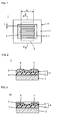
- Fig. 1 is a plan view showing a field-effect transistor 1 according to a first embodiment of the present invention.
- Fig. 2 is a magnified partial view of a section taken along the line II-II of Fig. 1 .
- the field-effect transistor 1 is provided with a substrate 2 formed from, for example, glass.
- a gate electrode 3 formed from, for example, gold or a metal primarily containing gold is disposed on the substrate 2.
- the two-dimensional shape of the gate electrode 3 is indicated by a broken line.
- a gate insulating film 4 is disposed on the substrate 2 in such a way as to cover the gate electrode 3. The gate insulating film 4 will be described later in detail.
- a source electrode 6 and a drain electrode 7 formed from, for example, gold or a metal primarily containing gold is disposed on the semiconductor film 5.
- the source electrode 6 and the drain electrode 7 take on mutually opposed interdigital shapes, and are arranged interdigitating with each other. This is for the purpose of maximizing a channel width W in a limited area.
- the channel length is a dimension indicated by L shown in Fig. 1 .
- the above-described gate insulating film 4 is characterized by being provided with a plurality of insulating layers including at least a first insulating layer 11 disposed in such a way as to contact the semiconductor film 5, wherein the first insulating layer 11 is composed of poly-p-xylylene, e.g., polydichloro-p-xylylene, formed by a CVD method in which a cyclophane, e.g., dichloro(2,2)-p-cyclophane, is used as a CVD material.
- poly-p-xylylene for example, A to F shown in Table 1 as described below can be used. [Table 1] Example of poly-p-xylylene A B C D E F
- the gate insulating film 4 is also provided with a second insulating layer 12 having a dielectric constant higher than that of the first insulating layer 11.
- film formation of the first insulating layer 11 is conducted by the CVD method and no solvent is used in the film formation. Therefore, regarding the second insulating layer 12, even a material easily affected by a solvent can be used without problems. Consequently, for example, cyanoethyl pullulan can be used as a material for the second insulating layer 12 with advantage. Since a film can be formed from a single component polymer solution containing no fine particle by using cyanoethyl pullulan, the second insulating layer 12 is allowed to become a film exhibiting good smoothness.
- the second insulating layer 12 may be formed from a resin containing a metal oxide powder, e.g., a barium titanate powder.
- a metal oxide powder e.g., a barium titanate powder.
- cyanoethyl pullulan containing a metal oxide powder may be used as the material for the second insulating layer 12.
- the first insulating layer 11 is formed into a film by the CVD method, no solvent is used, and a high purity CVD material is easily available. Therefore, the first insulating layer 11 is allowed to become a film having a low impurity content, and a stable high field-effect mobility can be ensured. Furthermore, the second insulating layer can be provided with a high dielectric constant and, thereby, the threshold voltage can be lowered. Moreover, an occurrence of mixing of impurities, which may be contained in the second insulating layer 12 provided in the gate insulating film 4, into the semiconductor film 5 is blocked by the first insulating layer 11 effectively, so that the on-off ratio can be increased.
- the thickness of the second insulating layer 12 is larger than the thickness of the first insulating layer 11.
- the thickness of the first insulating layer 11 is 50 nm or more. The reason for this is that if such a thickness is selected, the above-described impurities, which may be contained in the second insulating layer 12, are blocked by the first insulating layer 11 more reliably, and an occurrence of mixing into the semiconductor film 4 is prevented more reliably.
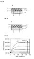
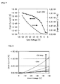
- Fig. 3 , Fig. 4, and Fig. 5 are diagrams showing field-effect transistors 1a, 1b, and 1c, respectively, according to the second, the third, and the fourth embodiments, respectively, of the present invention and corresponding to Fig. 2 .
- the elements corresponding to the elements shown in Fig. 2 are indicated by the same reference numerals as those in Fig. 2 , and explanations thereof are not repeated hereafter.
- the orders of lamination of elements are different from that in the field-effect transistor 1 shown in Fig. 2 .
- these field-effect transistors 1a, 1b, and 1c are commonly characterized in that the semiconductor film 5 is disposed in such a way as to contact the source electrode 6 and the drain electrode 7, the gate insulating film 4 is disposed between the gate electrode 3 and the semiconductor film 5, and the first insulating layer 11 is disposed in such a way as to contact the semiconductor film 5.
- a first insulating layer having a thickness of 50 nm composed of polydichloro-p-xylylene (relative dielectric constant was 3.2 at 1 kHz) serving as poly-p-xylylene was formed on the above-described second insulating layer by the CVD method, in which dichloro(2,2)-p-cyclophane serving as cyclophane was used as a raw material, at a reduced pressure of about 1.0 ⁇ 10 -2 Pa under the condition that the vaporization temperature of the raw material was 125°C, the decomposition temperature was 630°C, and the substrate temperature was room temperature.
- a semiconductor film having a thickness of 40 nm was formed on the above-described first insulating layer by evaporating pentacene at a reduced pressure of about 1.3 ⁇ 10 -4 Pa in terms of degree of vacuum under the condition that the rate was 0.3 ⁇ /sec and the substrate temperature was room temperature.
- This mask was disposed on the above-described semiconductor film, gold was evaporated at a reduced pressure of about 6.5 ⁇ 10 -4 Pa in terms of degree of vacuum under the condition that the rate was 1.0 ⁇ /sec and the substrate temperature was 25°C so as to form a source electrode and a drain electrode which had thicknesses of 30 nm and, thereby, obtain a field-effect transistor.
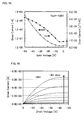
- the current-voltage characteristic of the resulting field-effect transistor was measured by using a semiconductor parameter analyzer ("4156C" produced by Agilent) so as to obtain the output characteristic shown in Fig. 6 .
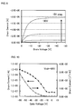
- the relationship between the gate voltage and the drain current in a saturation region based on the result of the output characteristic is indicated as the transfer characteristic shown in Fig. 7 .
- I d W / 2 ⁇ L ⁇ C i ⁇ ⁇ ⁇ V g - V t 2
- I d represents a drain current
- W represents a channel width
- L represents a channel length
- V g represents a gate voltage
- C i represents an insulating film capacity per unit area
- ⁇ represents a field-effect mobility
- V t represents a threshold voltage
- a ratio of a maximum value (on-current) of the drain current to a minimum value (off-current), that is, an on-off ratio, was 3.7 ⁇ 10 4 .
- Table 2 described below shows variations between field-effect transistors related to Samples 1 to 3 prepared at the same time.
- Sample No. Gate voltage at minimum drain current Minimum value of drain current (V) (A) 1 2 2.1 ⁇ 10 -7 2 0 7.3 ⁇ 10 -6 3 0 7.1 ⁇ 10 -6
- a field-effect transistor was prepared in a manner similar to that in Example 1 except that merely cyanoethyl pullulan was used in the formation of a gate insulating film and the resulting gate insulating film had a thickness of 1,090 nm and a single layer structure.
- three field-effect transistors related to Samples 4 and 5 having the same structure were prepared at the same time.
- the current-voltage characteristic of the resulting field-effect transistor was measured in a manner similar to that in Example 1 so as to obtain the output characteristic shown in Fig. 8 .
- Table 3 described below shows variations between field-effect transistors related to Samples 4 to 6 prepared at the same time.
- Sample No. Gate voltage at minimum drain current Minimum value of drain current (V) (A) 4 -22 9.1 ⁇ 10 -6 5 2 2.2 ⁇ 10 -4 6 -16 5.8 ⁇ 10 -7
- a field-effect transistor was prepared in a manner similar to that in Example 1 except that merely polydichloro-p-xylylene was used in the formation of a gate insulating film and the resulting gate insulating film had a thickness of 880 nm and a single layer structure.
- the current-voltage characteristic of the resulting field-effect transistor was measured in a manner similar to that in Example 1 so as to obtain the output characteristic shown in Fig. 9 and the transfer characteristic shown in Fig. 10 .
- Table 4 shows the material for each of the semiconductor film, the second insulating layer, and the first insulating layer, the threshold voltage, the on-off ratio, and variations between samples. Furthermore, regarding each of the materials for the second insulating layer and the first insulating layer, the relative dielectric constant is shown in parentheses.
- Comparative example 1 merely cyanoethyl pullulan was used for the gate insulating film. Therefore, as shown in Fig. 8 , no saturation region appeared.
- Example 1 as shown in Fig. 6 , the field-effect transistor exhibiting a large on-off ratio was obtained because in the gate insulating film, not only the second insulating layer composed of cyanoethyl pullulan, but also the first insulating layer composed of poly-p-xylylene was formed. Furthermore, regarding Example 1, the threshold voltage was reduced to one-fifth or less of the threshold voltage of Comparative example 2 in which merely poly-p-xylylene was used for the gate insulating film. Moreover, according to Example 1, variations in characteristic values between samples were small and, therefore, a stable field-effect transistor was able to be obtained.
- Example 1 it is estimated that in Example 1, the first insulating layer composed of poly-p-xylylene was thinner than the second insulating layer composed of cyanoethyl pullulan, the dielectric constant of the whole gate insulating film was maintained at a high level and, thereby, the threshold voltage was lowered.
- Comparative example 2 since the dielectric constant of poly-p-xylylene constituting the gate insulating film was low, a smaller current was passed as compared with that in Example 1 at the same gate voltage and, thereby, the threshold voltage was high.
- Example 2 a polyfluorene-thiophene copolymer (F8T2) was used as the material for a semiconductor film, and a sample related to each of Example 2 within the scope of the present invention and Comparative examples 3 and 4 out of the scope of the present invention was prepared.
- F8T2 polyfluorene-thiophene copolymer
- a second insulating layer having a thickness of 1,000 nm composed of cyanoethyl pullulan was formed on a glass substrate provided with a gate electrode formed from gold in a manner similar to that in Example 1.
- a first insulating layer having a thickness of 200 nm composed of polydichloro-p-xylylene was formed on the above-described second insulating layer by the CVD method, in which dichloro(2,2)-p-cyclophane was used as a raw material, at a reduced pressure of about 1.0 ⁇ 10 -2 Pa under the condition that the vaporization temperature of the raw material was 125°C, the decomposition temperature was 630°C, and the substrate temperature was 40°C.
- the above-described first insulating layer was spin-coated with a 0.6 percent by weight chloroform solution of polyfluorene-thiophene copolymer (F8T2), and a heat treatment was conducted at 60°C for 30 minutes, so that a semiconductor film having a thickness of 50 nm was formed.
- F8T2 polyfluorene-thiophene copolymer
- a source electrode and a drain electrode which had thicknesses of 30 nm were formed on the above-described semiconductor film in a manner similar to that in Example 1 and, thereby, a field-effect transistor was obtained.
- the current-voltage characteristic of the resulting field-effect transistor was measured in a manner similar to that in Example 1 so as to obtain the output characteristic shown in Fig. 11 and the transfer characteristic shown in Fig. 12 .
- a field-effect transistor was prepared in a manner similar to that in Example 2 except that merely cyanoethyl pullulan was used in the formation of a gate insulating film and the resulting gate insulating film had a thickness of 1,230 nm and a single layer structure.
- the current-voltage characteristic of the resulting field-effect transistor was measured in a manner similar to that in Example 1 so as to obtain the output characteristic shown in Fig. 13 .
- a field-effect transistor was prepared in a manner similar to that in Example 2 except that merely polydichloro-p-xylylene was used in the formation of a gate insulating film and the resulting gate insulating film had a thickness of 550 nm and a single layer structure.
- the current-voltage characteristic of the resulting field-effect transistor was measured in a manner similar to that in Example 1 so as to obtain the output characteristic shown in Fig. 14 and the transfer characteristic shown in Fig. 15 .
- Table 5 shows the material for each of the semiconductor film, the second insulating layer, and the first insulating layer, the threshold voltage, the on-off ratio, and variations between samples. The same evaluation method as that in the case of Table 4 described above was applied to the variations between samples.
- Example 2 According to Example 2, the same effects as those in Example 1 described above were obtained.
- a glass substrate provided with a gate electrode formed from gold was spin-coated with the above-described dispersion. Thereafter, heating was conducted at 100°C for 1 hour so as to form a second insulating layer having a thickness of 930 nm composed of barium titanate-containing cyanoethyl pullulan.
- the relative dielectric constant of barium titanate-containing cyanoethyl pullulan was 29.6 at 1 kHz.
- a first insulating layer having a thickness of 300 nm composed of polydichloro-p-xylylene was formed on the above-described second insulating layer in a manner similar to that in Example 2.
- a semiconductor film having a thickness of 40 nm was formed on the above-described first insulating layer in a manner similar to that in Example 1.
- a source electrode and a drain electrode which had thicknesses of 30 nm were formed on the above-described semiconductor film in a manner similar to that in Example 1 and, thereby, a field-effect transistor was obtained.
- the current-voltage characteristic of the resulting field-effect transistor was measured in a manner similar to that in Example 1 so as to obtain the output characteristic shown in Fig. 16 and the transfer characteristic shown in Fig. 17 .
- Table 6 shows the material for each of the semiconductor film, the second insulating layer, and the first insulating layer, the threshold voltage, the on-off ratio, and variations between samples. The same evaluation method as that in the case of Table 4 described above was applied to the variations between samples.
- Example 3 the same effects as those in Example 1 were obtained.
- the second insulating layer contained a high dielectric constant barium titanate powder, the dielectric constant of the whole gate insulating film increased, and the threshold voltage was lowered than that in Example 1.
- Example 4 an influence exerted by the thickness of the first insulating layer was examined.
- the following sample related to Example 4 within the scope of the present invention was prepared. That is, a field-effect transistor related to Example 4 having the same structure as the structure in Example 1 was prepared in a manner similar to the manner in Example 1 except that the thickness of the first insulating layer was specified to be 20 nm.
- the current-voltage characteristic of the resulting field-effect transistor was measured in a manner similar to that in Example 1 so as to obtain the output characteristic shown in Fig. 18 .
- the thickness of the first insulating layer is preferably 50 nm or more.
Landscapes
- Chemical & Material Sciences (AREA)
- Inorganic Chemistry (AREA)
- Engineering & Computer Science (AREA)
- Composite Materials (AREA)
- Materials Engineering (AREA)
- Thin Film Transistor (AREA)
Applications Claiming Priority (2)
| Application Number | Priority Date | Filing Date | Title |
|---|---|---|---|
| JP2006050245 | 2006-02-27 | ||
| PCT/JP2007/051557 WO2007097165A1 (ja) | 2006-02-27 | 2007-01-31 | 電界効果トランジスタ |
Publications (2)
| Publication Number | Publication Date |
|---|---|
| EP1990838A1 true EP1990838A1 (de) | 2008-11-12 |
| EP1990838A4 EP1990838A4 (de) | 2011-02-16 |
Family
ID=38437206
Family Applications (1)
| Application Number | Title | Priority Date | Filing Date |
|---|---|---|---|
| EP07713728A Ceased EP1990838A4 (de) | 2006-02-27 | 2007-01-31 | Feldeffekttransistor |
Country Status (4)
| Country | Link |
|---|---|
| US (1) | US7932177B2 (de) |
| EP (1) | EP1990838A4 (de) |
| JP (1) | JP5062435B2 (de) |
| WO (1) | WO2007097165A1 (de) |
Cited By (1)
| Publication number | Priority date | Publication date | Assignee | Title |
|---|---|---|---|---|
| WO2014020843A1 (en) * | 2012-08-01 | 2014-02-06 | Sony Corporation | Semiconductor device, display unit, and electronic apparatus |
Families Citing this family (2)
| Publication number | Priority date | Publication date | Assignee | Title |
|---|---|---|---|---|
| WO2009031525A1 (ja) * | 2007-09-07 | 2009-03-12 | Nec Corporation | カーボンナノチューブ構造物及び薄膜トランジスタ |
| US10388895B2 (en) * | 2017-11-07 | 2019-08-20 | Shenzhen China Star Optoelectonics Semiconductor Display Technology Co., Ltd. | Organic thin film transistor with charge injection layer and manufacturing method thereof |
Family Cites Families (9)
| Publication number | Priority date | Publication date | Assignee | Title |
|---|---|---|---|---|
| US6946676B2 (en) * | 2001-11-05 | 2005-09-20 | 3M Innovative Properties Company | Organic thin film transistor with polymeric interface |
| AU2002343058A1 (en) * | 2001-12-19 | 2003-06-30 | Merck Patent Gmbh | Organic field effect transistor with an organic dielectric |
| JP2004072049A (ja) * | 2002-08-09 | 2004-03-04 | Ricoh Co Ltd | 有機tft素子及びその製造方法 |
| KR100995451B1 (ko) | 2003-07-03 | 2010-11-18 | 삼성전자주식회사 | 다층 구조의 게이트 절연막을 포함하는 유기 박막 트랜지스터 |
| JP2005072569A (ja) * | 2003-08-06 | 2005-03-17 | Mitsubishi Chemicals Corp | 有機電界効果トランジスタ |
| JP4997688B2 (ja) * | 2003-08-19 | 2012-08-08 | セイコーエプソン株式会社 | 電極、薄膜トランジスタ、電子回路、表示装置および電子機器 |
| JP2005175386A (ja) * | 2003-12-15 | 2005-06-30 | Asahi Kasei Corp | 有機半導体素子 |
| KR20050080276A (ko) * | 2004-02-09 | 2005-08-12 | 삼성전자주식회사 | 박막 트랜지스터 표시판 및 그 제조 방법 |
| KR101133759B1 (ko) * | 2004-12-28 | 2012-04-09 | 삼성전자주식회사 | 전기 영동 표시 장치 및 그 제조 방법 |
-
2007
- 2007-01-31 JP JP2008501658A patent/JP5062435B2/ja not_active Expired - Fee Related
- 2007-01-31 WO PCT/JP2007/051557 patent/WO2007097165A1/ja not_active Ceased
- 2007-01-31 EP EP07713728A patent/EP1990838A4/de not_active Ceased
-
2008
- 2008-08-27 US US12/199,446 patent/US7932177B2/en not_active Expired - Fee Related
Non-Patent Citations (2)
| Title |
|---|
| ONOUE T ET AL: "LOW-OPERATING-VOLTAGE ORGANIC FIELD-EFFECT TRANSISTORS WITH POLY-P-XYLYLENE/HIGH-K POLYMER BILAYER GATE DIELECTRIC", JAPANESE JOURNAL OF APPLIED PHYSICS, JAPAN SOCIETY OF APPLIED PHYSICS, JP, vol. 45, no. 29, 21 July 2006 (2006-07-21) , pages L770-L772, XP001246307, ISSN: 0021-4922, DOI: DOI:10.1143/JJAP.45.L770 * |
| See also references of WO2007097165A1 * |
Cited By (3)
| Publication number | Priority date | Publication date | Assignee | Title |
|---|---|---|---|---|
| WO2014020843A1 (en) * | 2012-08-01 | 2014-02-06 | Sony Corporation | Semiconductor device, display unit, and electronic apparatus |
| CN104488104A (zh) * | 2012-08-01 | 2015-04-01 | 索尼公司 | 半导体器件、显示单元和电子装置 |
| TWI556452B (zh) * | 2012-08-01 | 2016-11-01 | 新力股份有限公司 | 半導體元件、顯示單元及電子裝置 |
Also Published As
| Publication number | Publication date |
|---|---|
| WO2007097165A1 (ja) | 2007-08-30 |
| JPWO2007097165A1 (ja) | 2009-07-09 |
| EP1990838A4 (de) | 2011-02-16 |
| US7932177B2 (en) | 2011-04-26 |
| US20090095954A1 (en) | 2009-04-16 |
| JP5062435B2 (ja) | 2012-10-31 |
Similar Documents
| Publication | Publication Date | Title |
|---|---|---|
| Xu et al. | Universal low-temperature Ohmic contacts for quantum transport in transition metal dichalcogenides | |
| KR100889796B1 (ko) | 비정질 산화물을 사용한 전계 효과 트랜지스터 | |
| EP2828892B1 (de) | Elektrisch leitfähige dünnschicht, beschichtungsflüssigkeit zur bildung der elektrisch leitfähigen dünnschicht, feldeffekttransistor und verfahren zur herstellung des feldeffekttransistors | |
| US9362313B2 (en) | Thin film transistor and display device | |
| US8043978B2 (en) | Electronic device and method for producing electronic device | |
| Lim et al. | Maxwell–Wagner model analysis for the capacitance–voltage characteristics of pentacene field effect transistor | |
| US10256091B2 (en) | Oxide for semiconductor layer of thin-film transistor, semiconductor layer of thin-film transistor having said oxide, and thin-film transistor | |
| WO2012074046A1 (ja) | 配線構造およびスパッタリングターゲット | |
| WO2012144556A1 (ja) | 薄膜トランジスタ構造、ならびにその構造を備えた薄膜トランジスタおよび表示装置 | |
| US10297465B2 (en) | Selective metal/metal oxide etch process | |
| US20190109199A1 (en) | Oxide semiconductor device | |
| Kim et al. | Dipole formation and electrical properties according to SiO2 layer thickness at an Al2O3/SiO2 interface | |
| CN101047130B (zh) | 使用纳米颗粒的顶栅薄膜晶体管及其制造方法 | |
| Ma et al. | Gate screening on remote phonon scattering for pentacene organic TFTs: Holes versus electrons | |
| US7932177B2 (en) | Field-effect transistor | |
| Kim et al. | Strontium doping effects on the characteristics of solution-processed aluminum oxide dielectric layer and its application to low-voltage-operated indium-gallium-zinc-oxide thin-film transistors | |
| CN108369962A (zh) | 薄膜晶体管及其制造方法以及具有所述薄膜晶体管的半导体装置 | |
| KR20180031979A (ko) | 산화물 박막트랜지스터 및 그 제조방법 | |
| JP2007273949A (ja) | ナノ粒子を用いたトップゲート型薄膜トランジスタおよびその製造方法 | |
| Takenaka et al. | Low-temperature formation of high-mobility a-InGaZnOx films using plasma-enhanced reactive processes | |
| Kabir et al. | Channel-length dependent performance degradation of thermally stressed IGZO TFTs | |
| Kato et al. | The characteristic improvement of Si (111) metal–oxide–semiconductor field-effect transistor by long-time hydrogen annealing | |
| KR20200126428A (ko) | 박막 트랜지스터를 유리 기판 상에 형성하는 방법 및 이로부터 형성된 액정 디스플레이 | |
| WO2019216209A1 (ja) | 酸化物半導体層を含む薄膜トランジスタ | |
| JP6742309B2 (ja) | トランジスタデバイスの生成方法 |
Legal Events
| Date | Code | Title | Description |
|---|---|---|---|
| PUAI | Public reference made under article 153(3) epc to a published international application that has entered the european phase |
Free format text: ORIGINAL CODE: 0009012 |
|
| 17P | Request for examination filed |
Effective date: 20080812 |
|
| AK | Designated contracting states |
Kind code of ref document: A1 Designated state(s): AT BE BG CH CY CZ DE DK EE ES FI FR GB GR HU IE IS IT LI LT LU LV MC NL PL PT RO SE SI SK TR |
|
| RIN1 | Information on inventor provided before grant (corrected) |
Inventor name: ONOUE, TOMOAKI Inventor name: YASUDA, TAKESHI Inventor name: TSUTSUI, TETSUO |
|
| A4 | Supplementary search report drawn up and despatched |
Effective date: 20110118 |
|
| DAX | Request for extension of the european patent (deleted) | ||
| 17Q | First examination report despatched |
Effective date: 20121105 |
|
| REG | Reference to a national code |
Ref country code: DE Ref legal event code: R003 |
|
| STAA | Information on the status of an ep patent application or granted ep patent |
Free format text: STATUS: THE APPLICATION HAS BEEN REFUSED |
|
| 18R | Application refused |
Effective date: 20160215 |