EP1990841A2 - Übergitter-Zugentlastungsschicht für Halbleitervorrichtungen - Google Patents
Übergitter-Zugentlastungsschicht für Halbleitervorrichtungen Download PDFInfo
- Publication number
- EP1990841A2 EP1990841A2 EP08014020A EP08014020A EP1990841A2 EP 1990841 A2 EP1990841 A2 EP 1990841A2 EP 08014020 A EP08014020 A EP 08014020A EP 08014020 A EP08014020 A EP 08014020A EP 1990841 A2 EP1990841 A2 EP 1990841A2
- Authority
- EP
- European Patent Office
- Prior art keywords
- layer
- gan
- substrate
- light emitting
- emitting diode
- Prior art date
- Legal status (The legal status is an assumption and is not a legal conclusion. Google has not performed a legal analysis and makes no representation as to the accuracy of the status listed.)
- Granted
Links
Images


Classifications
-
- H—ELECTRICITY
- H10—SEMICONDUCTOR DEVICES; ELECTRIC SOLID-STATE DEVICES NOT OTHERWISE PROVIDED FOR
- H10H—INORGANIC LIGHT-EMITTING SEMICONDUCTOR DEVICES HAVING POTENTIAL BARRIERS
- H10H20/00—Individual inorganic light-emitting semiconductor devices having potential barriers, e.g. light-emitting diodes [LED]
- H10H20/80—Constructional details
- H10H20/81—Bodies
- H10H20/811—Bodies having quantum effect structures or superlattices, e.g. tunnel junctions
-
- B—PERFORMING OPERATIONS; TRANSPORTING
- B82—NANOTECHNOLOGY
- B82Y—SPECIFIC USES OR APPLICATIONS OF NANOSTRUCTURES; MEASUREMENT OR ANALYSIS OF NANOSTRUCTURES; MANUFACTURE OR TREATMENT OF NANOSTRUCTURES
- B82Y20/00—Nanooptics, e.g. quantum optics or photonic crystals
-
- H—ELECTRICITY
- H10—SEMICONDUCTOR DEVICES; ELECTRIC SOLID-STATE DEVICES NOT OTHERWISE PROVIDED FOR
- H10H—INORGANIC LIGHT-EMITTING SEMICONDUCTOR DEVICES HAVING POTENTIAL BARRIERS
- H10H20/00—Individual inorganic light-emitting semiconductor devices having potential barriers, e.g. light-emitting diodes [LED]
- H10H20/80—Constructional details
- H10H20/81—Bodies
- H10H20/815—Bodies having stress relaxation structures, e.g. buffer layers
-
- H—ELECTRICITY
- H10—SEMICONDUCTOR DEVICES; ELECTRIC SOLID-STATE DEVICES NOT OTHERWISE PROVIDED FOR
- H10H—INORGANIC LIGHT-EMITTING SEMICONDUCTOR DEVICES HAVING POTENTIAL BARRIERS
- H10H20/00—Individual inorganic light-emitting semiconductor devices having potential barriers, e.g. light-emitting diodes [LED]
- H10H20/80—Constructional details
- H10H20/81—Bodies
- H10H20/822—Materials of the light-emitting regions
- H10H20/824—Materials of the light-emitting regions comprising only Group III-V materials, e.g. GaP
- H10H20/825—Materials of the light-emitting regions comprising only Group III-V materials, e.g. GaP containing nitrogen, e.g. GaN
-
- H—ELECTRICITY
- H10—SEMICONDUCTOR DEVICES; ELECTRIC SOLID-STATE DEVICES NOT OTHERWISE PROVIDED FOR
- H10P—GENERIC PROCESSES OR APPARATUS FOR THE MANUFACTURE OR TREATMENT OF DEVICES COVERED BY CLASS H10
- H10P14/00—Formation of materials, e.g. in the shape of layers or pillars
- H10P14/20—Formation of materials, e.g. in the shape of layers or pillars of semiconductor materials
- H10P14/29—Formation of materials, e.g. in the shape of layers or pillars of semiconductor materials characterised by the substrates
- H10P14/2901—Materials
- H10P14/2921—Materials being crystalline insulating materials
-
- H—ELECTRICITY
- H10—SEMICONDUCTOR DEVICES; ELECTRIC SOLID-STATE DEVICES NOT OTHERWISE PROVIDED FOR
- H10P—GENERIC PROCESSES OR APPARATUS FOR THE MANUFACTURE OR TREATMENT OF DEVICES COVERED BY CLASS H10
- H10P14/00—Formation of materials, e.g. in the shape of layers or pillars
- H10P14/20—Formation of materials, e.g. in the shape of layers or pillars of semiconductor materials
- H10P14/32—Formation of materials, e.g. in the shape of layers or pillars of semiconductor materials characterised by intermediate layers between substrates and deposited layers
- H10P14/3202—Materials thereof
- H10P14/3214—Materials thereof being Group IIIA-VA semiconductors
- H10P14/3216—Nitrides
-
- H—ELECTRICITY
- H10—SEMICONDUCTOR DEVICES; ELECTRIC SOLID-STATE DEVICES NOT OTHERWISE PROVIDED FOR
- H10P—GENERIC PROCESSES OR APPARATUS FOR THE MANUFACTURE OR TREATMENT OF DEVICES COVERED BY CLASS H10
- H10P14/00—Formation of materials, e.g. in the shape of layers or pillars
- H10P14/20—Formation of materials, e.g. in the shape of layers or pillars of semiconductor materials
- H10P14/32—Formation of materials, e.g. in the shape of layers or pillars of semiconductor materials characterised by intermediate layers between substrates and deposited layers
- H10P14/3242—Structure
- H10P14/3244—Layer structure
- H10P14/3251—Layer structure consisting of three or more layers
- H10P14/3252—Alternating layers, e.g. superlattice
-
- H—ELECTRICITY
- H10—SEMICONDUCTOR DEVICES; ELECTRIC SOLID-STATE DEVICES NOT OTHERWISE PROVIDED FOR
- H10P—GENERIC PROCESSES OR APPARATUS FOR THE MANUFACTURE OR TREATMENT OF DEVICES COVERED BY CLASS H10
- H10P14/00—Formation of materials, e.g. in the shape of layers or pillars
- H10P14/20—Formation of materials, e.g. in the shape of layers or pillars of semiconductor materials
- H10P14/34—Deposited materials, e.g. layers
- H10P14/3402—Deposited materials, e.g. layers characterised by the chemical composition
- H10P14/3414—Deposited materials, e.g. layers characterised by the chemical composition being group IIIA-VIA materials
- H10P14/3416—Nitrides
-
- H—ELECTRICITY
- H10—SEMICONDUCTOR DEVICES; ELECTRIC SOLID-STATE DEVICES NOT OTHERWISE PROVIDED FOR
- H10P—GENERIC PROCESSES OR APPARATUS FOR THE MANUFACTURE OR TREATMENT OF DEVICES COVERED BY CLASS H10
- H10P14/00—Formation of materials, e.g. in the shape of layers or pillars
- H10P14/20—Formation of materials, e.g. in the shape of layers or pillars of semiconductor materials
- H10P14/34—Deposited materials, e.g. layers
- H10P14/3438—Doping during depositing
- H10P14/3441—Conductivity type
- H10P14/3442—N-type
Definitions
- the present invention is related generally to the field of light emitting diode devices, and more specifically to an architecture for an improved high-Al content, low defect heterostructure quantum well surface emitting light emitting diode device.
- the nitrides have been used to fabricate visible wavelength light emitting diode active regions. They also exhibit a sufficiently high bandgap to produce devices capable of emitting light in the ultraviolet, for example wavelengths between 300 and 400 nanometers.
- InAlGaN systems have been developed and implemented in visible and UV spectrum light emitting diodes (LEDs), such as disclosed in U.S. Patent 6,875,627 to Bour et al ., which is incorporated herein by reference.
- These devices are typically formed on an Al 2 O 3 (sapphire) substrate, and comprise thereover a GaN:Si or AlGaN template layer, an AlGaN:Si/GaN superlattice structure for reducing optical leakage, an n-type electrode contact layer, a GaN n-type waveguide, an InGaN quantum well heterostructure active region, and a GaN p-type waveguide region.
- the complete device may also have deposited thereover a p-type AlGaN:Mg cladding layer and a capping layer below a p-type electrode.
- the performance of the nitride-based light emitting diode emitting in the ultraviolet (UV) is still far inferior to that of blue or green light emitting diode. It is particularly true that for the UV light emitting diodes, the nature of the substrate and template layer have a critical impact on the overall device performance. For example, electrical resistance between the structural layers of the device significantly effects optical output. While Al 2 O 3 (sapphire) as a substrate has numerous advantages, the AlGaN template layer formed over the typical Al 2 O 3 substrate posses high series resistance due to limited doping capabilities. Furthermore, the crystallographic structure of the device layers plays a key role in the device's operational characteristics, and the AlGaN template layer provides a relatively poor crystalline template.
- the dislocation densities in AlGaN or AIN template layers on sapphire are typically in the mid 10 9 to high 10 10 cm -2 range.
- the external quantum efficiencies of deep UV light emitting diodes in the 250 nm to 350 nm range are still below 2% even for the very best devices (external quantum efficiencies near 50% have been demonstrated for blue GaN-based LED structures).
- the high dislocation densities in AlGaN or AIN template layers on sapphire also pose significant problems for the light emitting diode device lifetimes.
- GaN epitaxial layers on sapphire substrates have proven to be a better template for InGaAlN film growth, providing excellent optoelectronic quality for visible light emitting diode devices and reasonable dislocation densities.
- the dislocation densities in GaN template layers on sapphire are typically in the low 10 9 to mid 10 7 cm -2 ranges. Accordingly, sapphire with a GaN template layer is the preferred foundation for visible GaN-based light emitting diodes.
- the output wavelength of the light emitting diode is inversely related to the Al content in the multiple quantum well heterostructure (MQWH) active region of the device.
- MQWH multiple quantum well heterostructure
- a UV InAlGaN heterostructure grown on GaN/sapphire is under tensile stress, which causes cracking of the AlGaN epitaxial layers when the critical layer thickness is exceeded.
- the critical thickness for an AlGaN film with a 50% aluminum mole fraction is about 20-50nm, which is much too thin for realizing a usable device structure in the deep UV. Efforts to provide strain relief to accommodate the lattice mismatch have heretofore proven unsuccessful or impractical.
- the present invention is directed to a GaN/AlN strain relief layer that enables the growth of crack-free thick AlGaN films with high aluminum content on a GaN/sapphire template.
- an ultraviolet InAlGaN light emitting diode heterostructure is grown on a GaN/sapphire template with a GaN/AlN short period superlattice (SPSL) strain relief layer.
- the short period superlattice strain relief layer enables the growth of a high-quality and crack-free high aluminum content InAlGaN MQWH active region, providing a light emitting diode capable of emitting in the deep UV wavelength range.
- the GaN/AlN short period superlattice strain relief layer may be formed in conditions (e.g., temperature and pressure) consistent with the growth of other layers of the device for efficient production.
- the deep UV light emitting diode may be flip-chip bonded onto a heatsink and the sapphire substrate removed by excimer laser lift-off.
- the absorbing GaN template layer and some or all of the GaN/AlN short period superlattice strain relief layer may also be removed, for example by dry-etching (e.g. by CAIBE). Removal of the GaN/sapphire template allows for improved light extraction through the UV-transparent AlGaN current spreading layer and results also in lower operating voltages due to the vertical device structure.
- a GaN/AlN strain relief layer enables the growth of low defect, relatively high Al-content films over a GaN/sapphire template useful for non-optical applications, such as the high electron mobility transistors (HEMTs) and the like.
- HEMTs high electron mobility transistors
- the present invention provides a semiconductor structure, comprising:
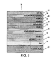
- Fig. 1 is a cross-sectional view of a multiple quantum-well heterostructure light emitting diode, including a GaN/AlN superlattice, according to an embodiment of the present invention.
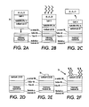
- Figs. 2A-2F are illustrations of the steps involved in a laser lift-off (LLO) and etch process to produce a surface-emitting light emitting diode according to an embodiment of the present invention.
- LLO laser lift-off
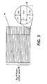
- Fig. 3 is a detailed view of a GaN/AlN superlattice structure according to an embodiment of the present invention.
- Fig. 4 is a scanning electron microscope (SEM) view of a partial multiple quantum-well heterostructure light emitting diode structure grown on GaN/sapphire template, including a GaN/AlN superlattice, according to an embodiment of the present invention.
- SEM scanning electron microscope
- Fig. 5 is a voltage versus current graph, showing acceptable device performance, for a deep UV light emitting diode grown on a GaN/sapphire template with a GaN/AlN superlattice strain relief structure according to the present invention.
- Fig. 6 is a graph of the Emission spectra (wavelength versus light output), for a deep UV light emitting diode grown on a GaN/sapphire template with a GaN/AlN superlattice strain relief structure according to the present invention.
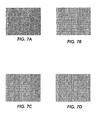
- Figs. 7A-7D are SEM micrographs of a deep UV emitting diode grown on a GaN/sapphire template with the number of layers comprising the superlattice strain relief structure at zero, 20, 40, 60, and 80 layer pairs of GaN/AlN, respectively.
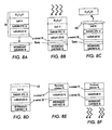
- Figs. 8A-8F are illustrations of the steps involved in a laser lift-off (LLO) and etch process to produce a surface-emitting light emitting diode according to another embodiment of the present invention.
- LLO laser lift-off
- Diode structure 10 comprises an Al 2 O 3 (sapphire) substrate 12 on which is formed a 2-10 micron thick epitaxial GaN template layer 14.
- GaN template layer 14 can be Si-doped or undoped and is typically grown at approximately 1100 degree C and a reactor pressure of approximately 200 Torr.
- Formed thereon is a GaN/AlN superlattice layer 16, described further below.
- AlGaN:Si buffer layer 18 Formed next is AlGaN:Si buffer layer 18, and formed thereon is AlGaN/AlGaN:Si superlattice n-strain layer 20 which allows for increased cladding thickness and hence reduced optical leakage of subsequent layers.
- AlGaN:Si n-cladding (index guiding) layer 22 Formed next is AlGaN:Si n-cladding (index guiding) layer 22.
- InAlGaN multiple quantum well active layer 24 is formed on layer 22.
- AlGaN:Mg p-cladding (index guiding) layer 26 Formed thereon is AlGaN:Mg p-cladding (index guiding) layer 26, then AlGaN:Mg buffer layer 28.
- AlGaN/AlGaN:Mg p-strain layer 30 is next deposited, then finally a GaN:Mg capping layer is formed over the structure.
- a complete device will also include electrodes, not shown, as well as other similar or alternative devices formed in the manner of an array in appropriate embodiments.
- the structure produced is a light emitting diode designed, for example, to emit UV light through the substrate. Since the GaN template layer is absorptive at UV wavelengths, optimal device performance may be obtained by removal of substrate 12 and GaN template layer 14. This may preferably be accomplished by the method, referred to herein as a laser lift-off (LLO) process, described in U.S. Patent 6,757,314 , which is incorporated by reference herein.
- LLO laser lift-off
- One embodiment of an LLO method bonds a combination substrate/heat sink to a surface opposite the Al 2 O 3 substrate.
- An excimer laser is typically employed to decouple the Al 2 O 3 substrate from the GaN layer, allowing removal of the substrate, the GaN layer is then removed by a chemical process (e.g., dry etch).
- GaN/AlN superlattice layer 16 is also removed by the chemical process at this point.
- a variation on this method first bonds an intermediate wafer to a surface opposite the Al 2 O 3 substrate.
- the Al 2 O 3 substrate and GaN layer are removed, and the device is then bonded to one of a variety of UV transparent substrates at the surface previously occupied by the GaN layer and Al 2 O 3 substrate.
- An example of such a process for removing the substrate and GaN template layer is illustrated in Figs. 2A-2F , which merely schematically illustrate the light emitting diode according to the present invention (i.e., not all layers thereof are shown in these figures.)
- a light emitting diode 34 (or an array of such devices) of a type described above is indirectly secured (e.g., flip-chip, thermally, or acoustically bonded) to a substrate 36 with high thermal conductivity (such as copper, diamond, bulk AIN, or silicon) to serve as a heat sink.
- the first metal contact 38 (p-contact) of the light emitting diode would be bonded to a solder 40/AuTi 42 layer pair on substrate/heatsink 36 (which may or may not be patterned), with the solder reflowing or deforming to form a permanent electrical, thermal, and mechanical contact/bond between the light emitting diode 34 and substrate/heat sink 36.
- the substrate/heatsink may be electrically conductive as well as thermally conductive, providing an electrical contact to the first contact 38 (p-contact) of the light emitting diode structure 34.
- an additional contact layer 44 may be placed on the backside of the substrate/heatsink 36 to improve electrical contacting.
- Fig. 2B With the light emitting diode structure 34 affixed to substrate/heatsink 36, an excimer laser is scanned over the Al 2 O 3 substrate 12. Due to the bandgap between GaN and its surrounding materials, there is high absorption of the light at the interface between the Al 2 O 3 substrate 12 and the GaN layer 14. This effectively results in decomposition of the GaN material at the sapphire/GaN interface, weakening or breaking the bond between the two layers. A second step to melt the transformed interface (typically at temperatures greater than the melting point of Ga (Tm - 30 C°) will further weaken the interface bond. With the bond sufficiently weakened, the Al 2 O 3 substrate 12 may simply be mechanically removed from the light emitting diode structure 34, as shown in Fig. 2C .
- the residual GaN layer 14 (typically several microns thick) and some or all of the GaN/AlN superlattice 16 are then removed using a dry etch (e.g., CAIBE) or possibly wet etching method.
- the structure is then substantially as shown in Fig. 2D .
- a second electrical contact 54 (n-contact) is then patterned directly on the exposed InAlGaN light emitting diode structure 52. This may be achieved in a variety of ways including (but not limited to) standard photolithography or a shadow mask processes.
- the structure is then as shown in Fig. 2E .
- the final light emitting diode structure 56 permits light extraction through an upper surface, and electrical contact directly to the light emitting diode active region via the contacts 44, 54 placed in direct contact on opposite sides of the active region.
- AIN is grown first upon GaN layer 14, then a layer of GaN, then another layer of AIN, and so forth with GaN as the final layer in the superlattice 16, and upon which AlGaN layer 18 is grown.
- Each of the superlattice pairs consists of an approximately 7 ⁇ wide GaN layer and an approximately 7 ⁇ wide AIN layer.
- the AIN and GaN layers are grown at approximately 1100 degree C° and approximately 200 Torr reactor pressure. The growth rate for the AIN and GaN layer was approximately ⁇ 0.5 ⁇ /sec.
- Superlattice layer 16 is nominally undoped, but could be doped (e.g., Si) by methods known in the art.
- GaN/AlN superlattice 16 a critical role of GaN/AlN superlattice 16 is to permit the incorporation of higher amounts of Al in subsequently deposited layers than previously possible, due to the reduced defects in layers deposited over superlattice 16.
- forming each component layer of the superlattice 16 requires setting of processing equipment controls and the introduction of constituent components, thus taking time and consuming processing resources. Therefore, there is a balance to be struck between growing a minimal number of layer pairs to simplify processing and a sufficient number of pairs to allow for a crack-free high Al content heterostructure.
- the number of GaN/AlN superlattice pairs was varied between 20 and 80.
- substrate 12, GaN template layer 14, and superlattice 16 were removed by processes described above and in aforementioned U.S. Patent 6,757,314 .
- the remaining completed devices were examined for structural integrity, and surface condition of AlGaN layer 18. (It is critical that AlGaN layer 18 be crack free so as to provide a suitable foundation for the subsequent layers, and further that the multiple quantum well heterostructure active layer be crack free for device performance.) Furthermore, optical performance of each device was measured.
- a 20 pair superlattice 16 produced a device which exhibited significant surface irregularity and cracks in the layer 18. Structural cracking decreased in structures with 40 superlattice pairs, but still showed some surface irregularity and cracks. Optimal results (freedom from structural cracks, surface smoothness, light emitting diode performance, minimal number of layer pairs) were obtained for a structure which included a superlattice 16 consisting of 80 GaN/AlN pairs. At 80 superlattice pairs layer 18 showed virtually no detectable damage or cracks. Table 1 summarizes these results. Figs. 7A-7D are SEM micrographs showing the visible results for this experiment.
- Fig. 4 shows a cross-sectional SEM image of a UV light emitting diode heterostructure 58, capable of emission at 325nm. Layers not specifically shown in Fig. 4 are either too thin to be seen in the SEM image or have low contrast (because of layer doping) as compared with nearby layers. (E.g. The contact layer on top of the structure is only 20nm and can not be seen in the SEM picture).
- Structure 58 includes an Al2O3 substrate 60, a GaN:Si template layer 62 formed on and over substrate 60, an 80 layer-pair GaN/AlN superlattice 64 formed on and over GaN:Si layer 62, and an InAlGaN multiple quantum well heterostructure layer 66 formed on and over superlattice 64.
- Each layer in superlattice 64 is approximately 7 ⁇ thick.
- the Al content in layer 66 was in the range of 35-40%. As can be seen, in cross section no cracks are visible in layer 66, a feature attributable to the provision of superlattice 64 thereunder.
- Fig. 5 device voltage versus current performance is shown for a deep UV light emitting diode grown on a GaN/sapphire template with a GaN/AlN superlattice strain relief structure according to the present invention (performance measured after removal of the substrate, etching of the GaN and GaN/AlN superlattice and transfer onto a quartz wafer) with peak emission around 327nm.
- Fig. 6 shown therein is the emission spectra of the UV light emitting diode whose voltage-current data is shown in Fig. 5 .
- the characterization data shows that after LLO and transfer of the device to a quartz substrate, the Deep UV LED still has good device performance, i.e. good IV performance, and narrow and clean emission spectra which indicate overall good material and device quality.
- a UV LED structure is transferred in fabrication from a sapphire substrate to UV transparent material/substrate via an intermediate host substrate.
- the intermediate host substrate may be quartz, a flex substrate that facilitates integration of the LED device into larger systems, etc.
- an intermediate (possibly UV transparent) substrate 70 is bonded to a surface of the UV LED structure opposite the sapphire substrate using an adhesive/epoxy, as shown in Fig. 8A .
- a LLO procedure is performed (as described previously), removing the sapphire substrate from the GaN layer, as shown in Figs. 8B and 8C .
- Etching then removes GaN layer 14 (optionally a sacrificial planarizaing layer 102 may be applied prior to etching), leaving the LED active region 52 (as well as additional layers) on the intermediate substrate, as shown in Fig. 8D .
- An n-contact layer 72 is then formed over the LED active region 52.
- Permanent substrate 74 is then bonded using a UV transparent epoxy (e.g., Epotek 301-2FL) to n-contact layer 72 (or alternatively, the substrate may form the n-contact, in which case substrate 74 is bonded directly to LED active region 52), as shown in Fig. 8E .
- a protective layer(s) may be applied to the lateral sides of the LED to insure the UV transparent epoxy does not bond with the intermediate substrate.
- the LED structure is released from the intermediate substrate 58 by emersion in a solvent (e.g., acetone) that dissolves the epoxy bonding the intermediate substrate 58 to the structure.
- Intermediate substrate 58 is then removed, leaving a device in which electrical contact is made from the top while light is extracted from the bottom of the device.
- intermediate substrate is UV transparent, and need not be removed. This also produces a device in which electrical contact is made from the top while the light is extracted from the bottom.
- a GaN/AlN strain relief layer formed over a GaN/sapphire template facilitates the formation of a substantially defect-free relatively high Al-content layer thereover. While particularly useful in optical systems, the present invention may also find applicability in non-optical systems.
- copending U.S. Patent application serial number 10/952,202 which is incorporated by reference herein, discloses high electron mobility transistors (HEMTs) in which a relatively high Al-content AlGaN buffer layer is formed below an undoped GaN layer.
- HEMTs high electron mobility transistors
- the provision of a GaN/AlN strain relief layer in such a system may provide an improved quality AlGaN layer and hence improved quality GaN layer, ultimately providing improved device performance.
- another embodiment of the present invention provides a GaN/AlN strain relief layer for the growth of low defect, relatively high Al-content films over a GaN/sapphire template useful for non-optical applications.
- a GaN/AlN superlattice is formed over a GaN/sapphire template to serve in part as a strain relief layer for growth of deep UV light emitting diodes. Furthermore, it has been demonstrated that a GaN/AlN superlattice can be successfully used to mitigate the strain between a GaN/sapphire template and a high Al mole fraction deep UV light emitting diode heterostructure. Deep UV light emitting diodes have successfully been grown using this technique and working light emitting diodes have been demonstrated, including devices having a substrate removed by excimer laser lift-off.
Landscapes
- Chemical & Material Sciences (AREA)
- Engineering & Computer Science (AREA)
- Nanotechnology (AREA)
- Physics & Mathematics (AREA)
- Life Sciences & Earth Sciences (AREA)
- Biophysics (AREA)
- Optics & Photonics (AREA)
- Crystallography & Structural Chemistry (AREA)
- Led Devices (AREA)
- Semiconductor Lasers (AREA)
Applications Claiming Priority (3)
| Application Number | Priority Date | Filing Date | Title |
|---|---|---|---|
| US73636205P | 2005-11-14 | 2005-11-14 | |
| US11/356,769 US7547925B2 (en) | 2005-11-14 | 2006-02-17 | Superlattice strain relief layer for semiconductor devices |
| EP06123849.9A EP1786044B1 (de) | 2005-11-14 | 2006-11-10 | Übergitter-Zugentlastungsschicht für Halbleitervorrichtungen |
Related Parent Applications (2)
| Application Number | Title | Priority Date | Filing Date |
|---|---|---|---|
| EP06123849.9A Division-Into EP1786044B1 (de) | 2005-11-14 | 2006-11-10 | Übergitter-Zugentlastungsschicht für Halbleitervorrichtungen |
| EP06123849.9A Division EP1786044B1 (de) | 2005-11-14 | 2006-11-10 | Übergitter-Zugentlastungsschicht für Halbleitervorrichtungen |
Publications (3)
| Publication Number | Publication Date |
|---|---|
| EP1990841A2 true EP1990841A2 (de) | 2008-11-12 |
| EP1990841A3 EP1990841A3 (de) | 2009-11-11 |
| EP1990841B1 EP1990841B1 (de) | 2020-01-08 |
Family
ID=37820657
Family Applications (2)
| Application Number | Title | Priority Date | Filing Date |
|---|---|---|---|
| EP08014020.5A Ceased EP1990841B1 (de) | 2005-11-14 | 2006-11-10 | Übergitter-Zugentlastungsschicht für Halbleitervorrichtungen |
| EP06123849.9A Active EP1786044B1 (de) | 2005-11-14 | 2006-11-10 | Übergitter-Zugentlastungsschicht für Halbleitervorrichtungen |
Family Applications After (1)
| Application Number | Title | Priority Date | Filing Date |
|---|---|---|---|
| EP06123849.9A Active EP1786044B1 (de) | 2005-11-14 | 2006-11-10 | Übergitter-Zugentlastungsschicht für Halbleitervorrichtungen |
Country Status (2)
| Country | Link |
|---|---|
| EP (2) | EP1990841B1 (de) |
| JP (1) | JP5255759B2 (de) |
Cited By (4)
| Publication number | Priority date | Publication date | Assignee | Title |
|---|---|---|---|---|
| US8088637B1 (en) | 2005-11-14 | 2012-01-03 | Palo Alto Research Center Incorporated | Method of manufacturing a semiconductor device including a superlattice strain relief layer |
| US9537054B2 (en) | 2014-04-15 | 2017-01-03 | Sensor Electronic Technology, Inc. | Semiconductor heterostructure with stress management |
| US9799793B2 (en) | 2014-04-15 | 2017-10-24 | Sensor Electronics Technology, Inc. | Semiconductor heterostructure with stress management |
| WO2021236729A1 (en) | 2020-05-19 | 2021-11-25 | Raxium, Inc. | Combination of strain management layers for light emitting elements |
Families Citing this family (16)
| Publication number | Priority date | Publication date | Assignee | Title |
|---|---|---|---|---|
| WO2008054995A2 (en) * | 2006-10-18 | 2008-05-08 | Nitek, Inc. | Vertical deep ultraviolet light emitting diodes |
| JP2010537408A (ja) * | 2007-08-14 | 2010-12-02 | ナイテック インコーポレイテッド | マイクロピクセル紫外発光ダイオード |
| KR101438808B1 (ko) | 2007-10-08 | 2014-09-05 | 엘지이노텍 주식회사 | 반도체 발광소자 및 그 제조방법 |
| JP5288852B2 (ja) * | 2008-03-21 | 2013-09-11 | スタンレー電気株式会社 | 半導体素子の製造方法 |
| EP2498282A4 (de) * | 2009-11-04 | 2014-06-25 | Dowa Electronics Materials Co Ltd | Epitaktisch beschichtetes gruppe-iii-nitrid-substrat |
| JP5334057B2 (ja) * | 2009-11-04 | 2013-11-06 | Dowaエレクトロニクス株式会社 | Iii族窒化物積層基板 |
| JP5353802B2 (ja) * | 2010-04-12 | 2013-11-27 | 豊田合成株式会社 | 半導体発光素子の製造方法およびランプ、電子機器、機械装置 |
| US8865565B2 (en) * | 2011-08-02 | 2014-10-21 | Kabushiki Kaisha Toshiba | LED having a low defect N-type layer that has grown on a silicon substrate |
| KR102237154B1 (ko) * | 2015-02-25 | 2021-04-07 | 엘지이노텍 주식회사 | 발광 소자 및 이를 구비한 라이트 유닛 |
| KR102416010B1 (ko) * | 2015-03-31 | 2022-07-05 | 서울바이오시스 주식회사 | 자외선 발광 소자 |
| KR102355604B1 (ko) * | 2015-07-03 | 2022-01-26 | 쑤저우 레킨 세미컨덕터 컴퍼니 리미티드 | 발광 소자 및 이를 구비한 라이트 유닛 |
| CN115881868B (zh) | 2016-04-15 | 2026-02-03 | 苏州立琻半导体有限公司 | 发光器件 |
| DE102016120335A1 (de) * | 2016-10-25 | 2018-04-26 | Osram Opto Semiconductors Gmbh | Halbleiterschichtenfolge und Verfahren zur Herstellung einer Halbleiterschichtenfolge |
| CN110473940B (zh) * | 2019-08-09 | 2024-05-17 | 晶能光电股份有限公司 | 紫外led的外延结构 |
| US11894489B2 (en) * | 2021-03-16 | 2024-02-06 | Epistar Corporation | Semiconductor device, semiconductor component and display panel including the same |
| CN115050866B (zh) * | 2022-08-16 | 2022-11-08 | 江苏第三代半导体研究院有限公司 | 极化可控的量子点Micro-LED同质外延结构及其制备方法 |
Citations (2)
| Publication number | Priority date | Publication date | Assignee | Title |
|---|---|---|---|---|
| US6757314B2 (en) | 1998-12-30 | 2004-06-29 | Xerox Corporation | Structure for nitride based laser diode with growth substrate removed |
| US6875627B2 (en) | 1999-09-29 | 2005-04-05 | Xerox Corporation | Structure and method for index-guided buried heterostructure AlGaInN laser diodes |
Family Cites Families (10)
| Publication number | Priority date | Publication date | Assignee | Title |
|---|---|---|---|---|
| JP3454181B2 (ja) * | 1999-03-23 | 2003-10-06 | 松下電器産業株式会社 | 窒化物半導体素子 |
| JP3773713B2 (ja) * | 1999-08-24 | 2006-05-10 | 三洋電機株式会社 | 量子箱の形成方法 |
| JP2001077412A (ja) * | 1999-09-02 | 2001-03-23 | Sanyo Electric Co Ltd | 半導体素子およびその製造方法 |
| JP2002100837A (ja) * | 2000-09-25 | 2002-04-05 | Sharp Corp | 窒化物半導体発光素子およびその製造方法 |
| US6906352B2 (en) * | 2001-01-16 | 2005-06-14 | Cree, Inc. | Group III nitride LED with undoped cladding layer and multiple quantum well |
| US6958497B2 (en) * | 2001-05-30 | 2005-10-25 | Cree, Inc. | Group III nitride based light emitting diode structures with a quantum well and superlattice, group III nitride based quantum well structures and group III nitride based superlattice structures |
| JP2003077835A (ja) * | 2001-09-06 | 2003-03-14 | Ngk Insulators Ltd | Iii族窒化物素子及びiii族窒化物エピタキシャル基板 |
| US20040140474A1 (en) * | 2002-06-25 | 2004-07-22 | Matsushita Electric Industrial Co., Ltd. | Semiconductor light-emitting device, method for fabricating the same and method for bonding the same |
| JP4438277B2 (ja) * | 2002-09-27 | 2010-03-24 | 日亜化学工業株式会社 | 窒化物半導体結晶の成長方法及びそれを用いた素子 |
| JP2005012063A (ja) * | 2003-06-20 | 2005-01-13 | Fujitsu Ltd | 紫外発光素子およびその製造方法 |
-
2006
- 2006-11-08 JP JP2006302240A patent/JP5255759B2/ja not_active Expired - Fee Related
- 2006-11-10 EP EP08014020.5A patent/EP1990841B1/de not_active Ceased
- 2006-11-10 EP EP06123849.9A patent/EP1786044B1/de active Active
Patent Citations (2)
| Publication number | Priority date | Publication date | Assignee | Title |
|---|---|---|---|---|
| US6757314B2 (en) | 1998-12-30 | 2004-06-29 | Xerox Corporation | Structure for nitride based laser diode with growth substrate removed |
| US6875627B2 (en) | 1999-09-29 | 2005-04-05 | Xerox Corporation | Structure and method for index-guided buried heterostructure AlGaInN laser diodes |
Non-Patent Citations (3)
| Title |
|---|
| CHEN ET AL., APPL. PHYS. LETT., vol. 81, 2002, pages 4961 |
| HAN ET AL., APPL. PHYS. LETT, vol. 78, 2001, pages 67 |
| NAKAMURA ET AL., J. J. APPL. PHYS., vol. 36, 1997, pages 1568 |
Cited By (8)
| Publication number | Priority date | Publication date | Assignee | Title |
|---|---|---|---|---|
| US8088637B1 (en) | 2005-11-14 | 2012-01-03 | Palo Alto Research Center Incorporated | Method of manufacturing a semiconductor device including a superlattice strain relief layer |
| US8154009B1 (en) | 2005-11-14 | 2012-04-10 | Palo Alto Research Center Incorporated | Light emitting structure including high-al content MQWH |
| US9537054B2 (en) | 2014-04-15 | 2017-01-03 | Sensor Electronic Technology, Inc. | Semiconductor heterostructure with stress management |
| US9735315B2 (en) | 2014-04-15 | 2017-08-15 | Sensor Electronic Technology, Inc. | Semiconductor heterostructure with stress management |
| US9799793B2 (en) | 2014-04-15 | 2017-10-24 | Sensor Electronics Technology, Inc. | Semiconductor heterostructure with stress management |
| US10199531B2 (en) | 2014-04-15 | 2019-02-05 | Sensor Electronic Technology, Inc. | Semiconductor heterostructure with stress management |
| WO2021236729A1 (en) | 2020-05-19 | 2021-11-25 | Raxium, Inc. | Combination of strain management layers for light emitting elements |
| EP4154325A4 (de) * | 2020-05-19 | 2024-06-26 | Google LLC | Kombination von belastungsverwaltungsschichten für lichtemittierende elemente |
Also Published As
| Publication number | Publication date |
|---|---|
| JP5255759B2 (ja) | 2013-08-07 |
| JP2007142397A (ja) | 2007-06-07 |
| EP1786044B1 (de) | 2016-01-20 |
| EP1990841B1 (de) | 2020-01-08 |
| EP1786044A1 (de) | 2007-05-16 |
| EP1990841A3 (de) | 2009-11-11 |
Similar Documents
| Publication | Publication Date | Title |
|---|---|---|
| US8154009B1 (en) | Light emitting structure including high-al content MQWH | |
| EP1990841B1 (de) | Übergitter-Zugentlastungsschicht für Halbleitervorrichtungen | |
| US10090435B2 (en) | III-nitride light emitting device including porous semiconductor | |
| KR102108196B1 (ko) | 성장 기판이 분리된 자외선 발광소자 및 그 제조 방법 | |
| US9905727B2 (en) | Fabrication of thin-film devices using selective area epitaxy | |
| US7501299B2 (en) | Method for controlling the structure and surface qualities of a thin film and product produced thereby | |
| TWI452717B (zh) | 成長於模板上以減少應變之iii族氮化物發光裝置 | |
| US8222670B2 (en) | Semiconductor light emitting element and method for manufacturing same | |
| KR20110055745A (ko) | 복합 기판 상에 성장되는 반도체 발광 장치 | |
| JP2007067418A (ja) | 二重ヘテロ構造の発光領域を有するiii族窒化物発光デバイス | |
| KR20100046241A (ko) | 에지 전위 템플릿 상에 성장된 ⅲ-질화물 디바이스 | |
| CN103636007A (zh) | 具有生长于硅基板上的低缺陷n型层的发光二极管 | |
| CN1290056A (zh) | 半导体元件及其制造方法 | |
| EP1881537A1 (de) | Nitrid-halbleiterelement und herstellungsverfahren dafür | |
| US7488667B2 (en) | Method for manufacturing nitride-base semiconductor element and nitride-base semiconductor element | |
| JP2023523546A (ja) | エピタキシャル側方過成長技法を使用してデバイスを除去するための方法 | |
| TW202234479A (zh) | 半導體基板、半導體基板之製造方法、半導體基板之製造裝置、電子零件及電子機器 | |
| KR20130139107A (ko) | 질화갈륨계 반도체 소자 및 그 제조방법 | |
| KR102147587B1 (ko) | 완화 층 상에 성장된 ⅲ-질화물 발광 디바이스 | |
| US7759219B2 (en) | Method of manufacturing nitride semiconductor device | |
| JP2015005534A (ja) | 縦型発光ダイオードおよび結晶成長方法 | |
| TWI649897B (zh) | 用於製造發光裝置的方法 | |
| JP2002009003A (ja) | 半導体基板およびその作製方法および発光素子 | |
| KR20190118798A (ko) | 입체 구조를 가지는 자외선 발광 소자 및 이의 제조방법 | |
| JP2009238834A (ja) | 窒化物系半導体層を有する支持基板およびその形成方法 |
Legal Events
| Date | Code | Title | Description |
|---|---|---|---|
| PUAI | Public reference made under article 153(3) epc to a published international application that has entered the european phase |
Free format text: ORIGINAL CODE: 0009012 |
|
| AC | Divisional application: reference to earlier application |
Ref document number: 1786044 Country of ref document: EP Kind code of ref document: P |
|
| AK | Designated contracting states |
Kind code of ref document: A2 Designated state(s): DE FR GB |
|
| PUAL | Search report despatched |
Free format text: ORIGINAL CODE: 0009013 |
|
| AK | Designated contracting states |
Kind code of ref document: A3 Designated state(s): DE FR GB |
|
| 17P | Request for examination filed |
Effective date: 20100511 |
|
| AKX | Designation fees paid |
Designated state(s): DE FR GB |
|
| 17Q | First examination report despatched |
Effective date: 20110908 |
|
| REG | Reference to a national code |
Ref country code: DE Ref legal event code: R079 Ref document number: 602006059047 Country of ref document: DE Free format text: PREVIOUS MAIN CLASS: H01L0033000000 Ipc: H01L0033120000 |
|
| RIC1 | Information provided on ipc code assigned before grant |
Ipc: H01L 33/32 20100101ALI20190516BHEP Ipc: H01L 33/12 20100101AFI20190516BHEP Ipc: H01L 33/04 20100101ALI20190516BHEP |
|
| GRAP | Despatch of communication of intention to grant a patent |
Free format text: ORIGINAL CODE: EPIDOSNIGR1 |
|
| INTG | Intention to grant announced |
Effective date: 20190705 |
|
| GRAS | Grant fee paid |
Free format text: ORIGINAL CODE: EPIDOSNIGR3 |
|
| GRAA | (expected) grant |
Free format text: ORIGINAL CODE: 0009210 |
|
| AC | Divisional application: reference to earlier application |
Ref document number: 1786044 Country of ref document: EP Kind code of ref document: P |
|
| AK | Designated contracting states |
Kind code of ref document: B1 Designated state(s): DE FR GB |
|
| REG | Reference to a national code |
Ref country code: GB Ref legal event code: FG4D |
|
| REG | Reference to a national code |
Ref country code: DE Ref legal event code: R096 Ref document number: 602006059047 Country of ref document: DE |
|
| REG | Reference to a national code |
Ref country code: DE Ref legal event code: R097 Ref document number: 602006059047 Country of ref document: DE |
|
| PLBE | No opposition filed within time limit |
Free format text: ORIGINAL CODE: 0009261 |
|
| STAA | Information on the status of an ep patent application or granted ep patent |
Free format text: STATUS: NO OPPOSITION FILED WITHIN TIME LIMIT |
|
| 26N | No opposition filed |
Effective date: 20201009 |
|
| PGFP | Annual fee paid to national office [announced via postgrant information from national office to epo] |
Ref country code: DE Payment date: 20201020 Year of fee payment: 15 Ref country code: GB Payment date: 20201021 Year of fee payment: 15 Ref country code: FR Payment date: 20201021 Year of fee payment: 15 |
|
| REG | Reference to a national code |
Ref country code: DE Ref legal event code: R119 Ref document number: 602006059047 Country of ref document: DE |
|
| GBPC | Gb: european patent ceased through non-payment of renewal fee |
Effective date: 20211110 |
|
| PG25 | Lapsed in a contracting state [announced via postgrant information from national office to epo] |
Ref country code: GB Free format text: LAPSE BECAUSE OF NON-PAYMENT OF DUE FEES Effective date: 20211110 Ref country code: DE Free format text: LAPSE BECAUSE OF NON-PAYMENT OF DUE FEES Effective date: 20220601 |
|
| PG25 | Lapsed in a contracting state [announced via postgrant information from national office to epo] |
Ref country code: FR Free format text: LAPSE BECAUSE OF NON-PAYMENT OF DUE FEES Effective date: 20211130 |