EP1990875A1 - Module optique bilateral monoconducteur - Google Patents
Module optique bilateral monoconducteur Download PDFInfo
- Publication number
- EP1990875A1 EP1990875A1 EP06714913A EP06714913A EP1990875A1 EP 1990875 A1 EP1990875 A1 EP 1990875A1 EP 06714913 A EP06714913 A EP 06714913A EP 06714913 A EP06714913 A EP 06714913A EP 1990875 A1 EP1990875 A1 EP 1990875A1
- Authority
- EP
- European Patent Office
- Prior art keywords
- photodiode
- laser diode
- stem
- lead pins
- optical
- Prior art date
- Legal status (The legal status is an assumption and is not a legal conclusion. Google has not performed a legal analysis and makes no representation as to the accuracy of the status listed.)
- Withdrawn
Links
Images






Classifications
-
- H—ELECTRICITY
- H01—ELECTRIC ELEMENTS
- H01S—DEVICES USING THE PROCESS OF LIGHT AMPLIFICATION BY STIMULATED EMISSION OF RADIATION [LASER] TO AMPLIFY OR GENERATE LIGHT; DEVICES USING STIMULATED EMISSION OF ELECTROMAGNETIC RADIATION IN WAVE RANGES OTHER THAN OPTICAL
- H01S5/00—Semiconductor lasers
- H01S5/02—Structural details or components not essential to laser action
- H01S5/022—Mountings; Housings
- H01S5/02208—Mountings; Housings characterised by the shape of the housings
- H01S5/02212—Can-type, e.g. TO-CAN housings with emission along or parallel to symmetry axis
-
- G—PHYSICS
- G02—OPTICS
- G02B—OPTICAL ELEMENTS, SYSTEMS OR APPARATUS
- G02B6/00—Light guides; Structural details of arrangements comprising light guides and other optical elements, e.g. couplings
- G02B6/24—Coupling light guides
- G02B6/42—Coupling light guides with opto-electronic elements
- G02B6/4201—Packages, e.g. shape, construction, internal or external details
- G02B6/4246—Bidirectionally operating package structures
-
- H—ELECTRICITY
- H01—ELECTRIC ELEMENTS
- H01S—DEVICES USING THE PROCESS OF LIGHT AMPLIFICATION BY STIMULATED EMISSION OF RADIATION [LASER] TO AMPLIFY OR GENERATE LIGHT; DEVICES USING STIMULATED EMISSION OF ELECTROMAGNETIC RADIATION IN WAVE RANGES OTHER THAN OPTICAL
- H01S5/00—Semiconductor lasers
- H01S5/02—Structural details or components not essential to laser action
- H01S5/022—Mountings; Housings
- H01S5/0225—Out-coupling of light
- H01S5/02251—Out-coupling of light using optical fibres
-
- H—ELECTRICITY
- H01—ELECTRIC ELEMENTS
- H01S—DEVICES USING THE PROCESS OF LIGHT AMPLIFICATION BY STIMULATED EMISSION OF RADIATION [LASER] TO AMPLIFY OR GENERATE LIGHT; DEVICES USING STIMULATED EMISSION OF ELECTROMAGNETIC RADIATION IN WAVE RANGES OTHER THAN OPTICAL
- H01S5/00—Semiconductor lasers
- H01S5/02—Structural details or components not essential to laser action
- H01S5/022—Mountings; Housings
- H01S5/023—Mount members, e.g. sub-mount members
- H01S5/02325—Mechanically integrated components on mount members or optical micro-benches
-
- H—ELECTRICITY
- H10—SEMICONDUCTOR DEVICES; ELECTRIC SOLID-STATE DEVICES NOT OTHERWISE PROVIDED FOR
- H10F—INORGANIC SEMICONDUCTOR DEVICES SENSITIVE TO INFRARED RADIATION, LIGHT, ELECTROMAGNETIC RADIATION OF SHORTER WAVELENGTH OR CORPUSCULAR RADIATION
- H10F77/00—Constructional details of devices covered by this subclass
- H10F77/50—Encapsulations or containers
-
- H—ELECTRICITY
- H10—SEMICONDUCTOR DEVICES; ELECTRIC SOLID-STATE DEVICES NOT OTHERWISE PROVIDED FOR
- H10W—GENERIC PACKAGES, INTERCONNECTIONS, CONNECTORS OR OTHER CONSTRUCTIONAL DETAILS OF DEVICES COVERED BY CLASS H10
- H10W72/00—Interconnections or connectors in packages
- H10W72/50—Bond wires
- H10W72/551—Materials of bond wires
- H10W72/552—Materials of bond wires comprising metals or metalloids, e.g. silver
- H10W72/5522—Materials of bond wires comprising metals or metalloids, e.g. silver comprising gold [Au]
-
- H—ELECTRICITY
- H10—SEMICONDUCTOR DEVICES; ELECTRIC SOLID-STATE DEVICES NOT OTHERWISE PROVIDED FOR
- H10W—GENERIC PACKAGES, INTERCONNECTIONS, CONNECTORS OR OTHER CONSTRUCTIONAL DETAILS OF DEVICES COVERED BY CLASS H10
- H10W90/00—Package configurations
- H10W90/701—Package configurations characterised by the relative positions of pads or connectors relative to package parts
- H10W90/751—Package configurations characterised by the relative positions of pads or connectors relative to package parts of bond wires
- H10W90/753—Package configurations characterised by the relative positions of pads or connectors relative to package parts of bond wires between laterally-adjacent chips
Definitions
- the present invention relates to a bi-directional optical module, and more particularly, to a bi-directional optical subassembly constituting the main part of the bi-directional optical module, and a transceiver which incorporates the subassembly.
- WDM wavelength division multiplexing
- PON passive optical network
- a bi-directional optical module for an optical line terminal (OLT) for transmitting on the wavelength of 1490 nm and receiving on the wavelength of 1310 nm for the central office, and a bi-directional optical module for an optical network unit (ONU) for transmitting on the wavelength of 1310 nm and receiving on the wavelength of 1490 nm for an end user are developing rapidly. Under such circumstances, there is a demand for compact, low-cost ONU modules in vast numbers.
- a bi-directional optical subassembly (hereinafter, referred to as "BOSA") constituting the main part of a bi-directional optical module usually include two packages for a laser diode (LD) and a photodiode (PD) (packaged individually with a can cap called "TO-CAN"), a fiber pigtail, a WDM filter, and a housing for holding the above components.
- the can cap for the LD and the can cap for the PD are positioned to form a right angle.
- Connecting pins for the LD and the PD also form a right angle. The distance between the pins must be long in order to reduce electric crosstalk between the transmitter and the receiver.
- Patent Document 1 United States Patent Application, Publication No. 2005/0084268
- an object of the present invention is to provide an optical module in which optical elements for transmitting and receiving are efficiently contained in a single TO-CAN package, and which can significantly improve (i.e., reduce) crosstalk that has been considered as unavoidable.
- a first aspect of the invention is a bi-directional optical subassembly, which includes: a laser diode; a photodiode; a stem for mounting the laser diode and the photodiode; a cap for sealing the laser diode and the photodiode, cooperating with the stem; and a crosstalk reducing structure for reducing optical and/or electric crosstalk.
- the crosstalk reducing structure includes a layer which is formed on an inner surface of the cap and is able to absorb the infrared ray.
- the layer includes a black-colored plating layer.
- a fourth aspect is characterized in that, in the second aspect, the layer includes a resin layer.
- the crosstalk reducing structure includes a block which is disposed between the laser diode and the photodiode, and is able to physically prevent stray light from the laser diode to the photodiode.
- the block includes a circuit board on which electronic parts (e.g., a laser diode and/or a photodiode) are mounted.
- a seventh aspect is characterized in that, in the first aspect, the crosstalk reducing structure includes resin which is disposed behind the laser diode and is able to absorb the light behind the LD.
- the bi-directional optical subassembly further includes a silicon substrate on which the laser diode and the photodiode are mounted, and the resin is provided on the silicon substrate.
- the stem includes a disk-shaped base, and a protruding part protruding vertically from the base and having a silicon substrate thereon on which the laser diode and the photodiode are mounted; and the resin is provided on the base of the stem.
- the stem includes a disk-shaped base, and a protruding part protruding vertically from the base and having a silicon substrate thereon on which the laser diode and the photodiode are mounted; and a group of transmitter lead pins and a group of receiver lead pins are provided to penetrate the stem; and a stem protruding part having ground potential is provided near the group of transmitter lead pins.
- the bi-directional optical subassembly further includes a transimpedance amplifier for amplifying a receiving signal from the photodiode
- the crosstalk reducing structure includes: a wire pair which connects the laser diode or an electrode pad connected thereto to the transmitter lead pin; a wire pair which connects the photodiode or an electrode pad connected thereto to the transimpedance amplifier; and a wire pair which connects the transimpedance amplifier to the receiver lead pin, and the wire pairs are provided to be substantially perpendicular to one another.
- the stem includes a disk-shaped base, and a protruding part protruding vertically from the base and having a silicon substrate thereon on which the laser diode and the photodiode are mounted; a plurality of lead pins for electrical connection which includes transmitter lead pins and receiver lead pins is provided to penetrate the stem; and the lead pins are divided into two groups, a group of transmitter lead pins and a group of receiver lead pins, at an opposite side of the stem protruding part, the lead pins are disposed parallel to one another, and a printed circuit board having a ground layer as an inner layer is provided between the groups of the lead pins.
- a thirteenth aspect is characterized in that, in the first aspect, the bi-directional optical subassembly further includes: a receptacle; and an optical filter provided at an optical input/output terminal on the receptacle at a cap side thereof, and is angled at a predetermined angle with respect to an optical axis.
- a fourteenth aspect is an optical transceiver, which includes: a bi-directional optical subassembly which includes: a laser diode, a photodiode, a cap for sealing the laser diode and the photodiode cooperating with a stem, and a crosstalk reducing structure for reducing optical and/or electric crosstalk; a printed circuit board which transmits and receives light for the bi-directional optical subassembly; and a casing for covering the bi-directional optical subassembly and the printed circuit board.
- the crosstalk reducing structure includes a layer which is formed on an inner surface of the cap and is able to absorb the infrared ray.
- a sixteenth aspect is characterized in that, in the fourteenth aspect, the crosstalk reducing structure includes a block which is disposed between the laser diode and the photodiode, and is able to physically prevent stray light from the laser diode to the photodiode.
- a seventeenth aspect is characterized in that, in the fourteenth aspect, the crosstalk reducing structure includes resin which is disposed behind the laser diode and is able to absorb the light behind the LD.
- the stem includes a disk-shaped base, and a protruding part protruding vertically from the base and having a silicon substrate thereon on which the laser diode and the photodiode are mounted; and a group of transmitter lead pins and a group of receiver lead pins are provided to penetrate the stem; and a stem protruding part having ground potential is provided near the group of transmitter lead pins.
- a nineteenth aspect is characterized in that, in the fourteenth aspect, the optical transceiver further includes a transimpedance amplifier for amplifying a receiving signal from the photodiode, and the crosstalk reducing structure includes: a wire pair which connects the laser diode or an electrode pad connected thereto to the transmitter lead pin; a wire pair which connects the photodiode or an electrode pad connected thereto to the transimpedance amplifier; and a wire pair which connects the transimpedance amplifier to the receiver lead pin, and the wire pairs are provided to be substantially perpendicular to one another.
- a twentieth aspect is characterized in that, in the fourteenth aspect, the optical transceiver further includes: a receptacle; and an optical filter provided at an optical input/output terminal on the receptacle at a cap side thereof, and is angled at a predetermined angle with respect to an optical axis.
- the number of components can be significantly reduced while maintaining or even improving its performance. Due to its simple structure and easy manufacture, the invention can be mass-produced at a lower cost.
- Fig. 1 is a perspective view of a micro-compact bi-directional optical subassembly (hereinafter, referred to as "micro-BOSA") 1 according to the present embodiment.
- Fig. 2A is a side view
- Fig. 2B is an end view of the micro-BOSA 1.
- Fig. 2C is a circuit diagram of the micro-BOSA 1.
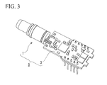
- Fig. 3 is a perspective view of an optical transceiver assembly 5 in which a printed circuit board 3 (used as a driver and as an electric interface) for transmitting and receiving is assembled to the micro-BOSA 1.
- Fig. 4A is a plan view, Fig.
- Fig. 4B is an end view
- Fig. 4C is a side view of the optical transceiver assembly 5.
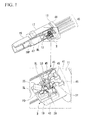
- Fig. 5 is a perspective view of an optical transceiver 6 with a predetermined casing 7.
- the optical transceiver 6 is a wavelength division multiplex (WDM) optical transceiver for transmitting and receiving on the wavelengths of 1310 nm and 1490 nm.
- WDM wavelength division multiplex
- the micro-BOSA 1 has successfully addressed the problems including stray light as described later with optical devices having at least optical bi-directional functions compactly accommodated in a single can cap (or package).
- the micro-BOSA 1 is about 16.4 mm in length and about 6.6 mm in diameter.
- the micro-BOSA is small enough to be accommodated in a conventional small form factor (SFF) transceiver package.
- the micro-BOAS 1 appears as a TO-coaxial optical subassembly (OSA).
- the micro-BOSA 1 essentially includes a micro-BOSA chip 9, a stem 11 on which the micro-BOSA chip 9 is mounted, a cap 13 with a ball lens for covering and sealing the micro-BOSA chip 9 (hereinafter, sometimes referred to as "can cap” or "TO-CAN"), a receptacle 15 (e.g., an SC optical connector) and a cylindrical connecting part 17 for connecting the can cap 13 to the receptacle 15.
- a receptacle 15 e.g., an SC optical connector
- cylindrical connecting part 17 for connecting the can cap 13 to the receptacle 15.
- the micro-BOSA chip 9 includes a silicon substrate 19 (e.g., silicon optical bench, SiOB) of 2.4 mm x 2.4 mm, and components to be mounted on the silicon substrate 19.
- the components include a laser diode LD chip, a photodiode PD chip, two silicon micro lenses SL, and a wavelength division multiplex filter (hereinafter, referred to as a "WDM filter") 25.
- the PD chip is mounted on the silicon substrate 19 via a glass substrate 27.
- a transimpedance amplifier (TIA) 29 and a ceramic substrate (i.e., a circuit board 31) are also mounted on the silicon substrate 19.
- the LD chip, the PD chip, and the WDM filter 25 can be mass-produced general parts manufactured at a low cost for conventional optical components.
- Two silicon micro lenses SL are diffraction lenses to provide a compact bi-directional function of space-coupling type.
- one of the silicon micro lenses SL is disposed between the LD chip and the WDM filter 25.
- the silicon micro lens SL may be an aspherical proximity lens for collimating light (e.g., 1310 nm) emitted from the LD chip.
- the other of the silicon micro lenses SL is disposed between the PD chip and the WDM filter 25.
- the silicon micro lens SL may be an aspherical proximity lens for converging light (e.g., 1490 nm) from the WDM filter 25 and introducing to the PD.
- A denotes an optical path for an output signal on the wavelength of 1310 nm
- B denotes an optical path for an input signal on the wavelength of 1490 nm.
- the silicon micro lenses SL can be produced with high precision at a low cost using conventional silicon LSI manufacturing technology.
- the silicon micro lenses SL are surface-mounted on corresponding V-grooves (not shown) provided on the silicon substrate 19 through passive alignment.
- the silicon micro lenses SL can be fixed in a highly precise manner with their side walls physically contacting the corresponding V-grooves.
- the PD of the present embodiment may be a PIN photodiode with an intrinsic semiconductor layer disposed between p-n junctions.
- the PD chip is mounted with its light receiving surface facing downward.
- the light passing through the lens at the PD side is slightly diffracted downward, converged and reflected on an end surface (mirror) of the V-groove. Then, the light is incident into the PD chip of an upper side.
- the present embodiment may also be applied to an OLT.
- the applicable scope of the invention may be readily broadened to a triplexer by merely adding an analog PD chip for video signals, a silicon micro lens, and another WDM filter to micro-BOSA chip of the present embodiment.
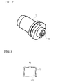
- the can cap 13 with a ball lens essentially includes a cylindrical (i.e., a can-shaped) cap body with a closed end, and a spherical ball lens BL fixed to penetrate at the center of the closed end.
- the ball lens BL functions as a coupling lens between the LD chip and the single mode optical fiber (SMF) placed within and connected to the receptacle 15.
- SMF single mode optical fiber
- the ball lens also functions as a coupling lens between the PD chip and the SMF. Since the ball lens functions as a shared coupling lens, optical axis adjustment (alignment) of both of the LD and the PD can be carried out by merely monitoring the light power of the LD output to the SMF, without monitoring the PD current.
- the stem 11 includes a stem disk part 41, a stem protruding part 43 extending from and substantially perpendicular to, the stem disk part 41, and multiple lead pins 45 provided to penetrate the stem disk part 41.
- the micro-BOSA chip 9 is mounted on the stem protruding part 43.
- the lead pins 45 arranged horizontally in a line above the center of the stem disk part 41 are receiver lead pins, and are numbered as N, P, VCC, and NC (spare) from the left.
- the lead pins 45 arranged horizontally in a line below the center of the stem 11 are transmitter lead pins, and are numbered as GND, LDK, and LDA from the left.
- the lead pins 45 and their corresponding parts are electrically connected by wire-bonded gold wires (see the thick solid lines in Fig. 1 ).
- the thus arranged lead pins 45 connect and fix the micro-BOSA 1 and the printed circuit board 3 together in a manner in which the lead pins 45 nip the printed circuit board 3 from above and below (see Fig. 4A and Fig. 4C ).
- One side of the printed circuit board 3 is used for optical transmitting circuits and the other side is used for optical receiving circuits (with this structure, individual chip set may be employed).
- a ground surface is provided in an intermediate layer of the printed circuit board 3. Since the optical transmitter system and the optical receiver system are separated by the ground layer of the printed circuit board 3, electric crosstalk can be reduced efficiently.
- the receptacle 15 is a connector for optically connecting the single mode optical fiber SMF and the ball lens BL.
- the receptacle 15 includes a fiber stub 47 made from, for example, zirconia ceramics for holding the SMF.
- a long wavelength cut-off filter (optical filter 49) for cutting light on the wavelengths longer than 1550 nm is attached to an input/output terminal at an end surface of the receptacle at a small cap side thereof. The end surface is angled at a predetermined angle.
- Ethernet registered trademark
- PON Ethernet
- light signals having other long wavelength such as analog video signals of 1550 nm, are delivered. With the structure described above, such light signals can be effectively prevented from reaching the PD or being reflected to the optical fiber. This advantageous effect can be obtained also in pigtail-shaped connectors.
- defects i.e., optical crosstalk (i.e., stray light)
- electric crosstalk i.e., optical crosstalk (i.e., stray light)
- defects i.e., optical crosstalk (i.e., stray light)
- electric crosstalk i.e., electric crosstalk
- first and second structures are provided in accordance with the invention. These structures may be used alone or in a superimposed state.
- the first structure includes a layer LYR provided on the inner surface of the can cap 13 for absorbing the infrared ray as shown in Fig. 8 .
- the layer LYR may be formed by plate processing, or by depositing resin.
- a film for absorbing the infrared ray i.e., stray light
- the plated layer absorbs the light emitted from the LD so as not to generate stray light.
- the thickness of the plated layer can be easily controlled. Thus, the plated layer can be made uniformly thin. Further, multiple cap processing may advantageously be done at a time.
- EPO-TEK H62 product name manufactured by Epoxy Technology Inc. of the United States has been proven suitable from several experiments.
- EPO-TEK H62 is an industrial functional bonding material used for C-MOS chip coating and ferrite fixing.
- EPO-TEK H62 is a black-colored, one-fluid material with aluminum filler.
- EPO-TEK H62 has excellent binding properties and moderate elasticity to any materials including ferrite and glass, and can be stored at room temperature. The above description of EPO-TEK H62 is citied from the resource of Daizo Corporation, Nichimoly Division.
- the second structure includes a block disposed between the transmitter LD and the receiver PD to physically intercept the stray light. Since the stray light is generated from the light emitted from the transmitter LD due to coupling loss between the transmitter LD and the lens, the block is provided to prevent the stray light to incident into the receiver PD. As can be seen in Fig. 9 , the above-mentioned ceramic substrate (i.e., circuit board 31) may function as the block. In Fig. 9 , the stray light is shown by bold arrow. With the second structure, the receiving properties can be improved due to reduced noise, and chips can be mounted densely on the substrate.
- a structure in which a one-layer circuit is formed to mount a capacitor for driving various ICs on an alumina ceramic substrate or an aluminum nitride ceramic substrate can be obtained.
- An LD driver of an optical network unit (ONU) used for passive optical network (PON) works in a burst mode.
- the output is controlled without using the monitor PD.
- No monitor PD is mounted in this structure.
- the light emitted behind the LD directly becomes stray light inside the can cap 13, which may be coupled to the receiver PD.
- the following two structures are provided in accordance with the invention so as to absorb the light behind the LD (i.e., stray light).
- the first structure is a potting structure, in which a designated resin is deposited on the stem 11 behind the LD, as shown in Fig. 10 .
- the designated resin is deposited on the silicon substrate 19 on which the LD is mounted behind the LD, as shown in Fig. 11 .
- the predetermined resin 53 provided behind the LD absorbs the light behind the LD effectively (in Figs. 10 and 11 , the arrow of thick solid line indicates stray light).
- the stray light heading for the receiver PD is significantly reduced, the stray light-induced noise is reduced, and the receiving property is significantly improved.
- the resin suitable for applying the inner surface of the can cap 13 may also be used here.
- Fig. 12 in the first structure, components are arranged in the can cap 13 such that bonding wires (wirings (gold wires) of the transmitter side) of the transmitter LD and bonding wires (wirings (gold wires) of the receiver side) of the receiver PD are positioned substantially perpendicular to each other.
- the thick solid lines in Fig. 12 indicate gold wires.
- transmitter lead pins 45 are provided below the surface of the silicon substrate 19 on the stem 11 (stem disk part 41) at the can cap side.
- the receiver lead pins 45 are provided above the surface of the silicon substrate 19. Ground constituting metal is provided near the transmitter lead pins. This structure can reduce electric crosstalk.
- a series of externally protruding lead pins 45 on the stem 11 (stem disk part 41) at the opposite side of the can cap 13 are divided into two groups: a group of receiver lead pins 45 (N, P, VCC and NC) (shown at the upper side in Fig. 13 ), and a group of transmitter lead pins 45 (LDK and LDA) and a lead pin 45 for grounding (shown at the lower side in the Fig. 13 ).
- the printed circuit board 3 having a grounding layer as an inner layer is disposed between the groups.
- Each lead pin 45 is connected and fixed to the printed circuit board 3 in a straightened state.
- an analog video signal (of e.g., 1550 nm) is cut off within the optical transceiver, the cut signal becomes stray light and then causes noise in digital receiving signals.
- a structure is provided in which the end surface of the receptacle is made as a polished surface angled at a predetermined angle (e.g., 6 to 8 degrees), and an analog video signal cut-off filter (a long wavelength cut-off filter 49) is attached to the end surface.
- the analog signal is reflected at the filter 49, directed toward a clad of the fiber SMF, and then absorbed in the fiber coating.
- the filter is formed inside the can cap, since the cut analog video signal is seldom introduced into the digital receiving system, and removed outside, the receiving quality of the digital signal is no longer influenced by the analog signal.
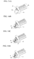
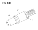
- FIG. 14A to 14H an exemplary manufacturing process of micro-BOSA 1 of the present embodiment will be described briefly.
- the inventors developed a prototype of the micro-BOSA in accordance with the invention and examined the optical and optoelectrical characteristics at 25°C. The resultant characteristics were desirable:
- the inventors also developed a prototype of an optical transceiver which incorporates the micro-BOSA in accordance with the invention, and examined its optical characteristics. As a result, it was proved that the optical transceiver had, in two-way communication at 1.25 Gbit/s, the minimum light-receiving sensitivity of -28.5 dBm which is low enough for use as a Gigabit Ethernet (registered trademark) PON transceiver. It is to be noted that the micro-BOSA can also be applied to the OLT.
- a micro-BOSA with a simple structure can be provided, which can be easily manufactured and successfully addresses the problems such as optical and electric crosstalk.
- the micro-BOSA contributes to further improvement in bi-directional optical communication.
Landscapes
- Physics & Mathematics (AREA)
- General Physics & Mathematics (AREA)
- Optics & Photonics (AREA)
- Condensed Matter Physics & Semiconductors (AREA)
- Electromagnetism (AREA)
- Semiconductor Lasers (AREA)
- Optical Couplings Of Light Guides (AREA)
- Light Receiving Elements (AREA)
Applications Claiming Priority (1)
| Application Number | Priority Date | Filing Date | Title |
|---|---|---|---|
| PCT/JP2006/303787 WO2007099612A1 (fr) | 2006-02-28 | 2006-02-28 | Module optique bilateral monoconducteur |
Publications (2)
| Publication Number | Publication Date |
|---|---|
| EP1990875A1 true EP1990875A1 (fr) | 2008-11-12 |
| EP1990875A4 EP1990875A4 (fr) | 2013-05-01 |
Family
ID=38458736
Family Applications (1)
| Application Number | Title | Priority Date | Filing Date |
|---|---|---|---|
| EP06714913.8A Withdrawn EP1990875A4 (fr) | 2006-02-28 | 2006-02-28 | Module optique bilateral monoconducteur |
Country Status (6)
| Country | Link |
|---|---|
| US (1) | US7917036B2 (fr) |
| EP (1) | EP1990875A4 (fr) |
| JP (1) | JP4713634B2 (fr) |
| KR (1) | KR101025267B1 (fr) |
| CN (1) | CN101385208B (fr) |
| WO (1) | WO2007099612A1 (fr) |
Cited By (2)
| Publication number | Priority date | Publication date | Assignee | Title |
|---|---|---|---|---|
| EP2806467A3 (fr) * | 2013-05-24 | 2015-03-11 | Oxford Instruments Analytical Oy | Tête de détecteur à semi-conducteur et son procédé de fabrication |
| EP2614604A4 (fr) * | 2010-09-06 | 2016-08-31 | Huawei Tech Co Ltd | Diminution de diaphonie dans un dispositif optoélectronique bidirectionnel |
Families Citing this family (48)
| Publication number | Priority date | Publication date | Assignee | Title |
|---|---|---|---|---|
| US8217482B2 (en) * | 2007-12-21 | 2012-07-10 | Avago Technologies General Ip (Singapore) Pte. Ltd. | Infrared proximity sensor package with reduced crosstalk |
| KR101426285B1 (ko) * | 2008-01-09 | 2014-08-05 | 삼성전자주식회사 | 광 송수신 소자 및 그 제조방법 |
| JP2009239197A (ja) * | 2008-03-28 | 2009-10-15 | Sumitomo Electric Ind Ltd | 光通信モジュール |
| JP5109833B2 (ja) * | 2008-06-25 | 2012-12-26 | 住友電気工業株式会社 | 光トランシーバ |
| US8145061B2 (en) * | 2009-01-13 | 2012-03-27 | Sumitomo Electric Industries, Ltd. | Optical module implementing a light-receiving device and a light-transmitting device within a common housing |
| US8420999B2 (en) * | 2009-05-08 | 2013-04-16 | Avago Technologies Ecbu Ip (Singapore) Pte. Ltd. | Metal shield and housing for optical proximity sensor with increased resistance to mechanical deformation |
| US9525093B2 (en) | 2009-06-30 | 2016-12-20 | Avago Technologies General Ip (Singapore) Pte. Ltd. | Infrared attenuating or blocking layer in optical proximity sensor |
| US8957380B2 (en) * | 2009-06-30 | 2015-02-17 | Avago Technologies General Ip (Singapore) Pte. Ltd. | Infrared attenuating or blocking layer in optical proximity sensor |
| US8779361B2 (en) * | 2009-06-30 | 2014-07-15 | Avago Technologies General Ip (Singapore) Pte. Ltd. | Optical proximity sensor package with molded infrared light rejection barrier and infrared pass components |
| US20110024627A1 (en) * | 2009-07-31 | 2011-02-03 | Avago Technologies Ecbu (Singapore) Pte. Ltd. | Proximity Sensor with Ceramic Housing and Light Barrier |
| US8716665B2 (en) * | 2009-09-10 | 2014-05-06 | Avago Technologies General Ip (Singapore) Pte. Ltd. | Compact optical proximity sensor with ball grid array and windowed substrate |
| US8350216B2 (en) * | 2009-09-10 | 2013-01-08 | Avago Technologies Ecbu Ip (Singapore) Pte. Ltd. | Miniaturized optical proximity sensor |
| US8143608B2 (en) * | 2009-09-10 | 2012-03-27 | Avago Technologies Ecbu Ip (Singapore) Pte. Ltd. | Package-on-package (POP) optical proximity sensor |
| JP5475404B2 (ja) * | 2009-11-12 | 2014-04-16 | 日本オクラロ株式会社 | チップキャリア及び光通信モジュール |
| US9733357B2 (en) * | 2009-11-23 | 2017-08-15 | Avago Technologies General Ip (Singapore) Pte. Ltd. | Infrared proximity sensor package with improved crosstalk isolation |
| KR101419381B1 (ko) | 2010-04-07 | 2014-07-15 | 한국전자통신연구원 | 양방향 광송수신 장치 |
| US8946877B2 (en) | 2010-09-29 | 2015-02-03 | Avago Technologies General Ip (Singapore) Pte. Ltd. | Semiconductor package including cap |
| US8841597B2 (en) | 2010-12-27 | 2014-09-23 | Avago Technologies Ip (Singapore) Pte. Ltd. | Housing for optical proximity sensor |
| CN102651667A (zh) * | 2011-02-25 | 2012-08-29 | 汪润泉 | 聚合物单纤光收发模组及其制备方法 |
| US8811824B2 (en) | 2011-09-15 | 2014-08-19 | Golfoton Holdings, Inc. | Two way burst mode digital optical cable communication system |
| US9331781B2 (en) | 2011-09-15 | 2016-05-03 | Go!Foton Corporation | Two way burst mode digital optical cable communication system |
| US10180547B2 (en) * | 2012-02-23 | 2019-01-15 | Taiwan Semiconductor Manufacturing Company, Ltd. | Optical bench on substrate |
| US9618712B2 (en) | 2012-02-23 | 2017-04-11 | Taiwan Semiconductor Manufacturing Company, Ltd. | Optical bench on substrate and method of making the same |
| US20130222908A1 (en) * | 2012-02-24 | 2013-08-29 | Xian-Li Yeh | Optically isolated to-can |
| KR101864708B1 (ko) * | 2012-08-28 | 2018-06-07 | 한국전자통신연구원 | 다채널 광수신 모듈 |
| CN102890313B (zh) * | 2012-10-22 | 2015-07-15 | 索尔思光电(成都)有限公司 | Cwdm多工/解多工器系统及其制造方法 |
| US9372315B2 (en) * | 2013-05-31 | 2016-06-21 | Futurewei Technologies, Inc. | Micro bi-directional optical sub-assembly |
| CN104459904B (zh) * | 2013-09-18 | 2016-05-04 | 福州高意通讯有限公司 | 一种单纤双向bosa结构 |
| KR20150145124A (ko) | 2014-06-18 | 2015-12-29 | 한국전자통신연구원 | 양방향 광송수신 모듈 및 이의 정렬방법 |
| JP6417199B2 (ja) * | 2014-12-08 | 2018-10-31 | 浜松ホトニクス株式会社 | 量子カスケードレーザ装置 |
| KR102017580B1 (ko) * | 2015-04-29 | 2019-09-05 | 주식회사 포벨 | 파장 가변 필터를 이용한 광 수신기 |
| JP2018139237A (ja) * | 2015-07-16 | 2018-09-06 | 三菱電機株式会社 | レーザモジュール |
| EP3410471B1 (fr) * | 2016-01-27 | 2025-04-02 | KYOCERA Corporation | Substrat de câblage, boîtier d'élément à semi-conducteur optique et dispositif à semi-conducteur optique |
| CN113296202B (zh) * | 2016-02-05 | 2022-10-21 | 苏州旭创科技有限公司 | 光模块 |
| US10197751B2 (en) * | 2016-03-17 | 2019-02-05 | Applied Optoelectronics, Inc. | Coaxial transmitter optical subassembly (TOSA) including ball lens |
| CN105871471A (zh) * | 2016-03-28 | 2016-08-17 | 青岛海信宽带多媒体技术有限公司 | 光模块 |
| US20170315313A1 (en) * | 2016-04-28 | 2017-11-02 | Futurewei Technologies, Inc. | Transistor Outline (TO) Can Optical Transceiver |
| TWI616076B (zh) * | 2016-09-30 | 2018-02-21 | 國立高雄應用科技大學 | 分波多工光收發器 |
| US10180544B2 (en) * | 2016-11-17 | 2019-01-15 | Corning Optical Communications LLC | Micro-optical systems and assemblies using glass tubes and methods of forming same |
| US10916912B2 (en) * | 2017-01-20 | 2021-02-09 | Mitsubishi Electric Corporation | Optical module |
| CN107222265A (zh) * | 2017-05-17 | 2017-09-29 | 西安科锐盛创新科技有限公司 | 光模块 |
| WO2019049482A1 (fr) * | 2017-09-08 | 2019-03-14 | 株式会社エンプラス | Prise de connexion électrique |
| US10461496B2 (en) * | 2017-11-07 | 2019-10-29 | Dermal Photonics Corporation | Self-aligning laser assembly |
| EP3710859B1 (fr) | 2018-04-28 | 2023-04-19 | SZ DJI Technology Co., Ltd. | Capteurs de détection de lumière et de télémétrie ayant plusieurs émetteurs et plusieurs récepteurs, et systèmes et procédés associés |
| WO2019205153A1 (fr) * | 2018-04-28 | 2019-10-31 | 深圳市大疆创新科技有限公司 | Module d'encapsulation de diode laser, appareil de transmission, appareil de télémétrie et dispositif électronique |
| US10451810B1 (en) * | 2018-08-22 | 2019-10-22 | Corning Optical Communications LLC | Adapter for electrically connecting a laser diode to a circuit board |
| JP2022116383A (ja) * | 2019-06-28 | 2022-08-10 | 京セラ株式会社 | 電子素子搭載用パッケージ及び電子装置 |
| CN116626819A (zh) * | 2022-02-14 | 2023-08-22 | 宁波环球广电科技有限公司 | 光模块 |
Family Cites Families (13)
| Publication number | Priority date | Publication date | Assignee | Title |
|---|---|---|---|---|
| JPH0427339U (fr) * | 1990-06-27 | 1992-03-04 | ||
| JPH0587973U (ja) * | 1992-04-24 | 1993-11-26 | 三菱電機株式会社 | 光半導体素子モジュール |
| CN2393272Y (zh) | 1999-09-25 | 2000-08-23 | 尚新民 | 一种抗阳光干扰的红外线探头 |
| TW594093B (en) | 1999-10-19 | 2004-06-21 | Terashima Kentaro | Optical transmission and reception system, and optical transmission and reception module and optical cable for the system |
| CN2513121Y (zh) | 2001-11-23 | 2002-09-25 | 鸿富锦精密工业(深圳)有限公司 | 固定光衰减器 |
| JP3862559B2 (ja) | 2001-11-30 | 2006-12-27 | シャープ株式会社 | 光送受信モジュールおよび電子機器 |
| JP3912111B2 (ja) * | 2002-01-09 | 2007-05-09 | 富士通株式会社 | 波長多重双方向光伝送モジュール |
| JP4015425B2 (ja) * | 2002-01-17 | 2007-11-28 | ローム株式会社 | 光送受信モジュール |
| JP2003344709A (ja) | 2002-05-23 | 2003-12-03 | Okano Electric Wire Co Ltd | ファイバ型光モジュール |
| KR100480252B1 (ko) * | 2002-10-10 | 2005-04-07 | 삼성전자주식회사 | 이중 캡 구조의 양방향 광송수신기 모듈 |
| GB0317858D0 (en) * | 2003-07-30 | 2003-09-03 | Denselight Semiconductors Pte | Optical transceiver |
| DE10348675B3 (de) | 2003-10-15 | 2005-06-09 | Infineon Technologies Ag | Modul für eine bidirektionale optische Signalübertragung |
| JP4828103B2 (ja) * | 2004-07-28 | 2011-11-30 | 三菱電機株式会社 | 光送受信モジュール |
-
2006
- 2006-02-28 JP JP2008502599A patent/JP4713634B2/ja not_active Expired - Lifetime
- 2006-02-28 WO PCT/JP2006/303787 patent/WO2007099612A1/fr not_active Ceased
- 2006-02-28 EP EP06714913.8A patent/EP1990875A4/fr not_active Withdrawn
- 2006-02-28 CN CN2006800533368A patent/CN101385208B/zh not_active Expired - Fee Related
- 2006-02-28 KR KR1020087020663A patent/KR101025267B1/ko not_active Expired - Fee Related
-
2008
- 2008-08-27 US US12/199,302 patent/US7917036B2/en not_active Expired - Fee Related
Cited By (2)
| Publication number | Priority date | Publication date | Assignee | Title |
|---|---|---|---|---|
| EP2614604A4 (fr) * | 2010-09-06 | 2016-08-31 | Huawei Tech Co Ltd | Diminution de diaphonie dans un dispositif optoélectronique bidirectionnel |
| EP2806467A3 (fr) * | 2013-05-24 | 2015-03-11 | Oxford Instruments Analytical Oy | Tête de détecteur à semi-conducteur et son procédé de fabrication |
Also Published As
| Publication number | Publication date |
|---|---|
| JPWO2007099612A1 (ja) | 2009-07-16 |
| WO2007099612A1 (fr) | 2007-09-07 |
| US20090129783A1 (en) | 2009-05-21 |
| CN101385208A (zh) | 2009-03-11 |
| US7917036B2 (en) | 2011-03-29 |
| JP4713634B2 (ja) | 2011-06-29 |
| KR20080087904A (ko) | 2008-10-01 |
| CN101385208B (zh) | 2012-07-18 |
| KR101025267B1 (ko) | 2011-03-29 |
| EP1990875A4 (fr) | 2013-05-01 |
Similar Documents
| Publication | Publication Date | Title |
|---|---|---|
| US7917036B2 (en) | Bi-directional optical module | |
| US9372315B2 (en) | Micro bi-directional optical sub-assembly | |
| KR100411577B1 (ko) | 광섬유 접속부 및 그것의 사용 방법 | |
| US6850658B2 (en) | Apparatus for coupling an optoelectronic device to a fiber optic cable and a microelectronic device, a system including the apparatus, and a method of forming the same | |
| KR100349598B1 (ko) | 실리콘 광벤치를 이용한 스몰 폼 팩터 광송수신 집적 모듈 | |
| JP3937911B2 (ja) | 光送受信モジュール及びこれを用いた光通信システム | |
| US6937786B2 (en) | Parallel multiwavelength optical subassembly | |
| US20100247043A1 (en) | Optical module and wavelength division multiplexing optical module | |
| US10295765B2 (en) | TO-Can photodiode package with integrated coupling member and exposed active region, and a receiver optical subassembly (ROSA) using the same | |
| JP2019184941A (ja) | 光サブアセンブリ及びその製造方法並びに光モジュール | |
| WO2004070428A2 (fr) | Procede et appareil pour ensemble de module emetteur/recepteur optique parallele | |
| CN106291836A (zh) | 混合集成式光学次模块 | |
| CN111684739A (zh) | 一种光收发模块的光学结构和封装结构以及操作方法 | |
| JP2005173043A (ja) | 多チャンネル光モジュール | |
| US8049159B2 (en) | Optical transmitter-receiver subassembly and optical transmitter-receiver module | |
| US5123067A (en) | Optical head capable of being fitted into a hybrid circuit | |
| US20040136660A1 (en) | Assembly for high-speed optical transmitter or receiver | |
| US20060133739A1 (en) | Silicon optical bench-based optical sub-assembly and optical transceiver using the same | |
| JP2005525587A (ja) | 光信号を回折および減衰させる方法 | |
| JPWO2007114053A1 (ja) | 一心双方向光送受信モジュール及びその製造方法 | |
| Masuko et al. | A low cost PON transceiver using single TO-CAN type micro-BOSA | |
| JP3452120B2 (ja) | 光モジュール及び光トランシーバ | |
| TWI339029B (en) | Single bi-directional optical subassembly | |
| CN116299889A (zh) | 一种收发集成bosa双向光组件和光模块 | |
| JP2005222003A (ja) | マウント、光部品、光送受信モジュール及び双方向光通信モジュール |
Legal Events
| Date | Code | Title | Description |
|---|---|---|---|
| PUAI | Public reference made under article 153(3) epc to a published international application that has entered the european phase |
Free format text: ORIGINAL CODE: 0009012 |
|
| 17P | Request for examination filed |
Effective date: 20080902 |
|
| AK | Designated contracting states |
Kind code of ref document: A1 Designated state(s): DE FR GB IT |
|
| DAX | Request for extension of the european patent (deleted) | ||
| RBV | Designated contracting states (corrected) |
Designated state(s): DE FR GB IT |
|
| A4 | Supplementary search report drawn up and despatched |
Effective date: 20130402 |
|
| RIC1 | Information provided on ipc code assigned before grant |
Ipc: G02B 6/42 20060101ALI20130325BHEP Ipc: H01L 31/02 20060101ALI20130325BHEP Ipc: H01S 5/022 20060101AFI20130325BHEP |
|
| STAA | Information on the status of an ep patent application or granted ep patent |
Free format text: STATUS: THE APPLICATION IS DEEMED TO BE WITHDRAWN |
|
| 18D | Application deemed to be withdrawn |
Effective date: 20131030 |