EP1990904A2 - Appareil d'alimentation électrique pour dispositif d'affichage à plasma - Google Patents
Appareil d'alimentation électrique pour dispositif d'affichage à plasma Download PDFInfo
- Publication number
- EP1990904A2 EP1990904A2 EP07123784A EP07123784A EP1990904A2 EP 1990904 A2 EP1990904 A2 EP 1990904A2 EP 07123784 A EP07123784 A EP 07123784A EP 07123784 A EP07123784 A EP 07123784A EP 1990904 A2 EP1990904 A2 EP 1990904A2
- Authority
- EP
- European Patent Office
- Prior art keywords
- voltage
- power supply
- electrodes
- output unit
- converter
- Prior art date
- Legal status (The legal status is an assumption and is not a legal conclusion. Google has not performed a legal analysis and makes no representation as to the accuracy of the status listed.)
- Withdrawn
Links
Images


Classifications
-
- G—PHYSICS
- G09—EDUCATION; CRYPTOGRAPHY; DISPLAY; ADVERTISING; SEALS
- G09G—ARRANGEMENTS OR CIRCUITS FOR CONTROL OF INDICATING DEVICES USING STATIC MEANS TO PRESENT VARIABLE INFORMATION
- G09G3/00—Control arrangements or circuits, of interest only in connection with visual indicators other than cathode-ray tubes
- G09G3/20—Control arrangements or circuits, of interest only in connection with visual indicators other than cathode-ray tubes for presentation of an assembly of a number of characters, e.g. a page, by composing the assembly by combination of individual elements arranged in a matrix no fixed position being assigned to or needed to be assigned to the individual characters or partial characters
- G09G3/22—Control arrangements or circuits, of interest only in connection with visual indicators other than cathode-ray tubes for presentation of an assembly of a number of characters, e.g. a page, by composing the assembly by combination of individual elements arranged in a matrix no fixed position being assigned to or needed to be assigned to the individual characters or partial characters using controlled light sources
- G09G3/28—Control arrangements or circuits, of interest only in connection with visual indicators other than cathode-ray tubes for presentation of an assembly of a number of characters, e.g. a page, by composing the assembly by combination of individual elements arranged in a matrix no fixed position being assigned to or needed to be assigned to the individual characters or partial characters using controlled light sources using luminous gas-discharge panels, e.g. plasma panels
- G09G3/288—Control arrangements or circuits, of interest only in connection with visual indicators other than cathode-ray tubes for presentation of an assembly of a number of characters, e.g. a page, by composing the assembly by combination of individual elements arranged in a matrix no fixed position being assigned to or needed to be assigned to the individual characters or partial characters using controlled light sources using luminous gas-discharge panels, e.g. plasma panels using AC panels
- G09G3/296—Driving circuits for producing the waveforms applied to the driving electrodes
-
- H—ELECTRICITY
- H02—GENERATION; CONVERSION OR DISTRIBUTION OF ELECTRIC POWER
- H02M—APPARATUS FOR CONVERSION BETWEEN AC AND AC, BETWEEN AC AND DC, OR BETWEEN DC AND DC, AND FOR USE WITH MAINS OR SIMILAR POWER SUPPLY SYSTEMS; CONVERSION OF DC OR AC INPUT POWER INTO SURGE OUTPUT POWER; CONTROL OR REGULATION THEREOF
- H02M3/00—Conversion of DC power input into DC power output
- H02M3/02—Conversion of DC power input into DC power output without intermediate conversion into AC
- H02M3/04—Conversion of DC power input into DC power output without intermediate conversion into AC by static converters
-
- H—ELECTRICITY
- H02—GENERATION; CONVERSION OR DISTRIBUTION OF ELECTRIC POWER
- H02M—APPARATUS FOR CONVERSION BETWEEN AC AND AC, BETWEEN AC AND DC, OR BETWEEN DC AND DC, AND FOR USE WITH MAINS OR SIMILAR POWER SUPPLY SYSTEMS; CONVERSION OF DC OR AC INPUT POWER INTO SURGE OUTPUT POWER; CONTROL OR REGULATION THEREOF
- H02M3/00—Conversion of DC power input into DC power output
- H02M3/22—Conversion of DC power input into DC power output with intermediate conversion into AC
- H02M3/24—Conversion of DC power input into DC power output with intermediate conversion into AC by static converters
- H02M3/28—Conversion of DC power input into DC power output with intermediate conversion into AC by static converters using discharge tubes with control electrode or semiconductor devices with control electrode to produce the intermediate AC
- H02M3/325—Conversion of DC power input into DC power output with intermediate conversion into AC by static converters using discharge tubes with control electrode or semiconductor devices with control electrode to produce the intermediate AC using devices of a triode or a transistor type requiring continuous application of a control signal
- H02M3/335—Conversion of DC power input into DC power output with intermediate conversion into AC by static converters using discharge tubes with control electrode or semiconductor devices with control electrode to produce the intermediate AC using devices of a triode or a transistor type requiring continuous application of a control signal using semiconductor devices only
- H02M3/33507—Conversion of DC power input into DC power output with intermediate conversion into AC by static converters using discharge tubes with control electrode or semiconductor devices with control electrode to produce the intermediate AC using devices of a triode or a transistor type requiring continuous application of a control signal using semiconductor devices only with automatic control of the output voltage or current, e.g. flyback converters
- H02M3/33515—Conversion of DC power input into DC power output with intermediate conversion into AC by static converters using discharge tubes with control electrode or semiconductor devices with control electrode to produce the intermediate AC using devices of a triode or a transistor type requiring continuous application of a control signal using semiconductor devices only with automatic control of the output voltage or current, e.g. flyback converters with digital control
-
- H—ELECTRICITY
- H04—ELECTRIC COMMUNICATION TECHNIQUE
- H04N—PICTORIAL COMMUNICATION, e.g. TELEVISION
- H04N5/00—Details of television systems
- H04N5/66—Transforming electric information into light information
-
- G—PHYSICS
- G09—EDUCATION; CRYPTOGRAPHY; DISPLAY; ADVERTISING; SEALS
- G09G—ARRANGEMENTS OR CIRCUITS FOR CONTROL OF INDICATING DEVICES USING STATIC MEANS TO PRESENT VARIABLE INFORMATION
- G09G2330/00—Aspects of power supply; Aspects of display protection and defect management
- G09G2330/02—Details of power systems and of start or stop of display operation
- G09G2330/028—Generation of voltages supplied to electrode drivers in a matrix display other than LCD
-
- G—PHYSICS
- G09—EDUCATION; CRYPTOGRAPHY; DISPLAY; ADVERTISING; SEALS
- G09G—ARRANGEMENTS OR CIRCUITS FOR CONTROL OF INDICATING DEVICES USING STATIC MEANS TO PRESENT VARIABLE INFORMATION
- G09G2330/00—Aspects of power supply; Aspects of display protection and defect management
- G09G2330/04—Display protection
-
- G—PHYSICS
- G09—EDUCATION; CRYPTOGRAPHY; DISPLAY; ADVERTISING; SEALS
- G09G—ARRANGEMENTS OR CIRCUITS FOR CONTROL OF INDICATING DEVICES USING STATIC MEANS TO PRESENT VARIABLE INFORMATION
- G09G3/00—Control arrangements or circuits, of interest only in connection with visual indicators other than cathode-ray tubes
- G09G3/20—Control arrangements or circuits, of interest only in connection with visual indicators other than cathode-ray tubes for presentation of an assembly of a number of characters, e.g. a page, by composing the assembly by combination of individual elements arranged in a matrix no fixed position being assigned to or needed to be assigned to the individual characters or partial characters
- G09G3/22—Control arrangements or circuits, of interest only in connection with visual indicators other than cathode-ray tubes for presentation of an assembly of a number of characters, e.g. a page, by composing the assembly by combination of individual elements arranged in a matrix no fixed position being assigned to or needed to be assigned to the individual characters or partial characters using controlled light sources
- G09G3/28—Control arrangements or circuits, of interest only in connection with visual indicators other than cathode-ray tubes for presentation of an assembly of a number of characters, e.g. a page, by composing the assembly by combination of individual elements arranged in a matrix no fixed position being assigned to or needed to be assigned to the individual characters or partial characters using controlled light sources using luminous gas-discharge panels, e.g. plasma panels
- G09G3/288—Control arrangements or circuits, of interest only in connection with visual indicators other than cathode-ray tubes for presentation of an assembly of a number of characters, e.g. a page, by composing the assembly by combination of individual elements arranged in a matrix no fixed position being assigned to or needed to be assigned to the individual characters or partial characters using controlled light sources using luminous gas-discharge panels, e.g. plasma panels using AC panels
- G09G3/291—Control arrangements or circuits, of interest only in connection with visual indicators other than cathode-ray tubes for presentation of an assembly of a number of characters, e.g. a page, by composing the assembly by combination of individual elements arranged in a matrix no fixed position being assigned to or needed to be assigned to the individual characters or partial characters using controlled light sources using luminous gas-discharge panels, e.g. plasma panels using AC panels controlling the gas discharge to control a cell condition, e.g. by means of specific pulse shapes
- G09G3/293—Control arrangements or circuits, of interest only in connection with visual indicators other than cathode-ray tubes for presentation of an assembly of a number of characters, e.g. a page, by composing the assembly by combination of individual elements arranged in a matrix no fixed position being assigned to or needed to be assigned to the individual characters or partial characters using controlled light sources using luminous gas-discharge panels, e.g. plasma panels using AC panels controlling the gas discharge to control a cell condition, e.g. by means of specific pulse shapes for address discharge
-
- H—ELECTRICITY
- H02—GENERATION; CONVERSION OR DISTRIBUTION OF ELECTRIC POWER
- H02M—APPARATUS FOR CONVERSION BETWEEN AC AND AC, BETWEEN AC AND DC, OR BETWEEN DC AND DC, AND FOR USE WITH MAINS OR SIMILAR POWER SUPPLY SYSTEMS; CONVERSION OF DC OR AC INPUT POWER INTO SURGE OUTPUT POWER; CONTROL OR REGULATION THEREOF
- H02M1/00—Details of apparatus for conversion
- H02M1/0083—Converters characterised by their input or output configuration
- H02M1/009—Converters characterised by their input or output configuration having two or more independently controlled outputs
Definitions
- the present invention relates to plasma display devices and, more particularly, to a power supply for a plasma display device.
- a plasma display device typically includes a plasma display panel (PDP) that uses plasma generated by a gas discharge process to display characters or images.
- PDP plasma display panel
- the PDP can include, depending on its size, up to millions of pixels arranged in a matrix pattern.
- duration of a frame for driving all of the pixels of a PDP is divided into a plurality of subfields, each having a weight.
- Gray scales are expressed by the combination of weights of those subfields, from among all the subfields, at which a discharge is generated and a display operation is conducted.
- Turn-on/turn-off cells i.e., cells to be turned on or off
- a sustain discharge operation is performed in the turn-on cells so as to display an image during a sustain period.
- a conventional plasma display device includes two power supplies to generate voltages having different levels that are applied to the turn-on and turn-off cells during the address period. Since it is difficult to reduce the number of constituent elements and increase integration in such a configuration, a power supply for supplying at least two voltages by using a single voltage generator has been suggested.
- the power supply for supplying at least two voltages by using a single voltage generator has a quick current response speed so that an integrated circuit receiving the voltage generated by the voltage generator problematically generates heat, and therefore easily deteriorates the integrated circuit.
- a plasma display device and a power supply thereof, are provided for generating a plurality of voltages by using one single voltage generating circuit and reducing circuit deterioration caused by heat.
- a power supply for driving a plasma display device comprises a power supply unit, a first output unit, a second output unit, and a converter.
- the power supply unit has a switching transistor connected to a primary coil of a transformer adapted to transform an input voltage and to supply power to a first secondary coil and a second secondary coil of the transformer in response to an operation of the switching transistor.
- the first output unit includes the first secondary coil of the transformer and is adapted to output a first voltage and a second voltage lower than the first voltage.
- the first and second voltages are generated at the first secondary coil.
- the second output unit includes the second secondary coil of the transformer and is adapted to output a third voltage generated at the second secondary coil.
- the converter is coupled to the first output unit and adapted to convert the first voltage into a fourth voltage and to output the second voltage as a fifth voltage lower than the fourth voltage.
- the converter includes a pulse width modulation controller, a converter output unit, and a converter feedback signal generator.
- the pulse width modulation controller is adapted to convert the first voltage in response to a level of a sixth voltage and to output an AC voltage.
- the converter output unit is connected to the pulse width modulation controller and has a fourth coil configured to receive the AC voltage at a first terminal of the fourth coil and a first capacitor having a first terminal connected to a second terminal of the fourth coil.
- the fourth coil and the first capacitor are adapted to rectify the AC voltage and to generate the fourth voltage.
- the converter feedback signal generator is adapted to generate the sixth voltage from the fourth voltage and to transmit the sixth voltage to the pulse width modulation controller.
- the power supply may further comprise a power supply feedback signal generator and a switching controller.
- the power supply feedback signal generator is connected to the first output unit and to the second output unit and adapted to receive the third voltage and the fifth voltage and to generate a feedback signal.
- the switching controller is connected between the power supply feedback signal generator and the power supply unit and adapted to control a turn-on/off operation of the switching transistor in response to the feedback signal.
- the fifth voltage may be lower than the first voltage.
- the first voltage may be a ground voltage.
- the sixth voltage may be lower than the first voltage.
- a second aspect of the invention provides a plasma display device comprising first electrodes, second electrodes, and third electrodes formed in a direction crossing the first electrodes and the second electrodes, a sustain electrode driver adapted to drive the first electrodes, a scan electrode driver adapted to drive the second electrodes, an address electrode driver adapted to drive the third electrodes, a controller, and a power supply according to the first aspect of the invention.
- the controller is adapted to control the sustain electrode driver, the scan electrode driver, and the address electrode driver.
- the power supply is adapted to supply power to the sustain electrode driver, the scan electrode driver, and the address electrode driver.
- the input voltage of the power supply may be a seventh voltage higher than an eighth voltage, wherein the seventh voltage and the eighth voltage are alternately applied to the first electrodes during a sustain period.
- the fifth voltage may be a scan voltage sequentially applied to the first electrodes during an address period.
- wall charges mentioned in the following description mean charges formed and accumulated on a wall (e.g., a dielectric layer) close to an electrode of a discharge cell.
- a wall charge will be described as being “formed” or “accumulated” on the electrode, although the wall charges do not actually touch the electrodes.
- a wall voltage means a potential difference formed on the wall of the discharge cell by the wall charge.
- a plasma display device includes a PDP 100, a controller 200, an address electrode driver 300, a scan electrode driver 400, a sustain electrode driver 500, and a power supply 600.
- the PDP 100 includes a plurality of address electrodes A1 to Am extending in a column direction, and a plurality of sustain and scan electrodes X1 to Xn and Y1 to Yn in pairs extending in a row direction.
- the sustain electrodes X1 to Xn are formed in respective correspondence to the scan electrodes Y1 to Yn, and ends of the sustain electrodes X1 to Xn are connected in common.
- the PDP 100 includes a substrate (not shown) having the sustain and scan electrodes X1 to Xn and Y1 to Yn, and a substrate (not shown) having the address electrodes A1 to Am.
- the two substrates are arranged to face each other with a discharge space between them so that the scan electrodes Y1 to Yn and the sustain electrodes X1 to Xn may cross the direction of the address electrodes A1 to Am. Discharge spaces provided at crossing regions of the address electrodes, A, and sustain and scan electrodes, X and Y, form discharge cells.
- the above-described structure for the plasma display panel 100 is an example, and other panel structures may also be used in the embodiments of the present invention.
- the controller 200 receives external video signals, and outputs an address driving control signal Sa, a sustain electrode driving control signal Sx, and a scan electrode driving control signal Sy. In addition, the controller 200 divides a frame into a plurality of subfields. Each subfield has a reset period, an address period, and a sustain period.
- the address electrode driver 300 After receiving the address driving control signal Sa from the controller 200, the address electrode driver 300 applies a display data signal for selecting the discharge cells to be used in forming the image to the corresponding address electrodes A1 to Am.
- the scan electrode driver 400 receives the scan electrode driving control signal Sy from the controller 200, and applies a driving voltage to the scan electrode Y.
- the sustain electrode driver 500 receives the sustain electrode driving control signal Sx from the controller 200, and applies a driving voltage to the sustain electrode X.
- the power supply 600 provides a power source for driving the plasma display device to the controller 200, and the drivers 300, 400, 500.
- FIG. 2 shows a diagram representing driving waveforms of the plasma display device according to one exemplary embodiment of the present invention.
- the driving waveforms for one subfield of the PDP 100 shown in FIG. 1 are illustrated, and the one subfield includes the reset, address, and sustain periods.
- Variation of the voltage applied to the sustain X, scan Y and address A electrodes is controlled by the controller 200 shown in FIG. 1 .
- the voltages applied to the electrodes determine the reset, address and sustain operations.
- the reset period includes a rising period and a falling period.
- a voltage at the scan electrode Y is gradually increased from a Vs voltage to a Vset voltage. Since the voltage at the scan electrode Y is increased, a weak discharge is generated between the scan electrode Y and the sustain electrode X and between the scan electrode Y and the address electrode A. Therefore, (-) wall charges are formed on the scan electrode Y, and (+) wall charges are formed on the sustain electrode X and the address electrode A.
- a state of each cell is initialized during the reset period, and therefore the Vset voltage is set high enough to generate a discharge in the cell.
- the voltage at the scan electrode Y is increased or decreased in a ramp pattern.
- the waveform is not limited to a ramp pattern and the voltage applied may gradually increase in another manner, e.g. logarithmically.
- the voltage at the scan electrode Y is gradually decreased from the Vs voltage to the Vnf voltage. Since the voltage at the scan electrode Y is decreased, a weak discharge is generated between the scan electrode Y and the sustain electrode X and between the scan electrode Y and the address electrode A. Therefore, most of the (-) wall charges formed on the scan electrode Y and the (+) wall charges formed on the sustain and address electrodes X and A during the rising period are eliminated. Accordingly, the (-) wall charges on the scan electrode Y and the (+) wall charges on the sustain electrode X and the address electrode A are reduced.
- the (+) wall charge on the address electrode A is reduced to a degree sufficient for performing an address operation.
- the voltage of (Vnf-Ve) is set to be the firing voltage Vfxy between the scan electrode Y and the sustain electrode X. Accordingly, the wall voltage between the scan electrode Y and the sustain electrode X becomes almost 0V, and the cells to be turned off in the address period are prevented from being misfired in the sustain period.
- At least one falling period of the reset period is included in each subfield.
- the rising period may be optional for some subfields.
- a control program of the controller 200 shown in FIG. 1 determines whether the rising period is included in a particular subfield.
- a scan pulse having a VscL voltage i.e., a scan voltage
- an address voltage Va is applied to the address electrode A that passes through the light emitting cell among a plurality of cells formed by the scan electrode Y receiving the VscL voltage.
- the (+) wall charges are formed on the scan electrode Y and the (-) wall charges are formed on the respective address and sustain electrodes A and X.
- the VscL voltage is set to be equal to or lower than the Vnf voltage.
- a VscH voltage (i.e., a non-scan voltage) that is higher than the VscL voltage is applied to the scan electrodes Y not receiving the VscL voltage, and a reference voltage is applied to the address electrodes A of the discharge cells that are not selected as turn-on cells.
- a sustain pulse alternately having a high level voltage (the Vs voltage shown in FIG. 2 ) and a low level voltage (the 0V voltage shown in FIG. 2 ) is alternately applied to the scan electrode Y and the sustain electrode X. That is, the OV voltage is applied to the sustain electrode X when the Vs voltage is applied to the scan electrode Y, and the OV voltage is applied to the scan electrode Y when the Vs voltage is applied to the sustain electrode X, and a discharge is generated between the scan electrode Y and the sustain electrode X by the Vs voltage and the wall voltage that is formed between the scan electrode Y and the sustain electrode X by the address discharge.
- the sustain pulse is applied to the scan electrode Y and the sustain electrode X a number of times that corresponds to a weight of the corresponding subfield.
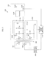
- a scan electrode driving voltage generator according to the exemplary embodiments of the present invention in the power supply 600 shown in FIG. 1 will now be described with reference to FIG. 3 .
- FIG. 3 shows a diagram representing the scan electrode driving voltage generator 610 according to an exemplary embodiment of the present invention.
- the scan electrode driving voltage generator 610 includes a power supply unit 611, a scan voltage generator 612, a driver voltage generator 613, a feedback signal generator 614, and a switching controller 615.
- the feedback signal generator 614 may also be referred to as a power supply feedback generator 614.
- the power supply unit 611 includes a primary coil L1 of a transformer 620 and a switching transistor Qsw coupled to the primary coil L1.
- the power supply unit 611 receives the Vs voltage and provides power to a secondary side of the transformer 620 (i.e., the scan voltage generator 612 and the driver voltage generator 613) according to duty cycle of the switching transistor Qsw.
- the scan voltage generator 612 includes a reference voltage generator 6122 and a converter 6124.
- the reference voltage generator 6122 may be referred to as a first output unit 6122.
- the driver voltage generator 613 may also be referred to as a second output unit 613.
- the reference voltage generator 6122 includes a secondary coil L2 of the transformer, a diode D1 having its anode coupled to a terminal of the secondary coil L2, a capacitor C1 having one terminal coupled to a cathode of the diode D1, and a resistor R1 including a terminal coupled to a common node between the diode D1 and the capacitor C1 and another terminal coupled to the other terminal of the capacitor C1.
- the reference voltage generator 6122 uses the diode D1 and the capacitor C1 to convert a voltage, which is induced from the primary coil L1 and generated at the secondary coil L2 according to a turn-on/off operation of the switching transistor Qsw, to a direct current voltage, and outputs the direct current voltage as a reference voltage GND.
- the converter 6124 for generating and outputting the VscH voltage and the VscL voltage includes two input terminals each coupled to one of the two terminals of a capacitor C2.
- the capacitor C2 is coupled in parallel with the capacitor C1.
- the converter 6124 uses a voltage input through the reference voltage generator 6122 to output the scan voltages VscH and VscL.
- the driver voltage generator 613 for generating a power source voltage of the scan electrode driver 400 shown in FIG. 1 includes a secondary coil L3 of the transformer 620, a diode D2 having its anode coupled to a terminal of the secondary coil L3, and a capacitor C3 coupled between a cathode of the diode D2 and a ground.
- a voltage applied between the two terminals of the capacitor C3 is a scan electrode driver driving voltage Vccf.
- the feedback voltage Vccf is output from the driver voltage generator 613.
- the secondary coil L2 of the reference voltage generator 6122 may be referred to as a first secondary coil L2 and the secondary coil L3 of the driver voltage generator 613 may be referred to as a second secondary coil L3.
- the feedback signal generator 614 is coupled to output terminals of the converter 6124 and the driver voltage generator 613, receives output voltages of the converter 6124 and the driver voltage generator 613, and generates a feedback signal.
- the switching controller 615 receives the feedback signal generated by the feedback signal generator 614, and controls the turn-on/off operation of the switching transistor Qsw in the power supply unit 611 to control output voltages of the scan voltage generator 612 and the driver voltage generator 613.
- the converter 6124 in the scan voltage generator 612 will now be described with reference to FIG. 4 .
- FIG. 4 shows a schematic diagram of the converter 6124 according to an exemplary embodiment of the present invention.
- the converter 6124 is a non-isolated switching mode power supply (SMPS). It includes a pulse width modulation (PWM) controller 61242, an converter output unit 61244, a converter feedback signal generator 61246, and a bias voltage supply unit 61248.
- PWM pulse width modulation
- the PWM controller 61242 may be realized by one integrated circuit (IC), and it includes four input terminals including a drain terminal D, a source terminal S, a bypass terminal BP, and a feedback terminal FB.
- the PWM controller 61242 may also include a PWM switching transistor (not shown), and a PWM switching controller (not shown) for controlling a turn-on/off operation of the PWM switching transistor.
- the drain terminal D for receiving an input voltage Vin of the converter 6124 is coupled to a node of the capacitor C1 and the capacitor C2 ( FIG. 3 ).
- the source terminal S outputs an output signal to the converter output unit 61244 according to the turn-on/off operation of the PWM switching transistor (not shown).
- the bypass terminal BP is coupled to the bias voltage supply unit 61248 and receives a driving voltage of the PWM switching controller (not shown) for controlling the turn-on/off operation of the PWM switching transistor (not shown).
- the feedback terminal FB receives a feedback voltage from the converter feedback signal generator 61246.
- the converter output unit 61244 includes a diode D4 including a cathode coupled to the source terminal S of the PWM controller 61242, an inductor L4 including a terminal coupled to the cathode of the diode D4, a capacitor C5 including a terminal coupled to another terminal of the inductor L4 and another terminal coupled to an anode of the diode D1, and a resistor R4 coupled in parallel to the two terminals of the capacitor C5.
- a higher voltage is the VscH voltage
- a lower voltage is the VscL voltage.
- the converter feedback signal generator 61246 includes a diode D3 having its anode coupled to one terminal of the inductor L4 in the converter output unit 61244, a capacitor C6 including a terminal coupled to a cathode of the diode D3 and a second terminal coupled to the other terminal of the inductor L4, a resistor R2 including a terminal coupled to the node formed between the cathode of the diode D3 and the capacitor C6 and another terminal coupled to the feedback terminal FB of the PWM controller 61242, and a resistor R3 including a terminal coupled to the feedback terminal FB of the PWM controller 61242 and another terminal coupled to a node formed between the source terminal S of the PWM controller ra1242 and the cathode of the diode D4.
- the converter feedback signal generator 61246 rectifies a voltage applied to the inductor L4 in the converter output unit 61244 by using the diode D3 and the capacitor C6, divides the rectified voltage by using the resistors R2 and R3, and transmits the divided voltages to the feedback terminal FB of the PWM controller 61242.
- the bias voltage supply unit 61248 includes a capacitor C4 having one terminal coupled to the source terminal S of the PWM controller 61242 and another terminal coupled to the bypass terminal BP.
- the bias voltage supply unit 61248 uses the input voltage Vin input through the drain terminal D when the PWM switching transistor (not shown) of the PWM controller 61242 is turned off, charges the capacitor C4 coupled to the bypass terminal BP, and drives the PWM switching controller (not shown) of the PWM controller 61242 for controlling the PWM switching transistor (not shown).
- the converter 6124 includes a feedback loop through the converter feedback signal generator 61246, and therefore, the VscH voltage and the VscL voltage may be precisely controlled.
- the converter output unit 61244 of the converter 6124 rectifies an AC voltage, which is output from the PWM controller 61242, by the inductor L4 and the capacitor C5, and outputs the scan voltages VscH, VscL having different voltage levels by the resistor R4.
- the inductor L4 delays outputting the voltage. The duration of delay may be predetermined. Accordingly, a response speed of the scan voltages VscH and VscL output through the scan electrode driving voltage generator according to the exemplary embodiment of the present invention is reduced.
- an isolated switching mode power supply using a transformer including at least two inductors may be used for the reference voltage generator 6122 rather than using the non-isolated switching mode power supply.
- generation of heat and circuit deterioration may be reduced or prevented, and the scan voltages VscH and VscL may be controlled.
- the scan electrode driving voltage generator may be used as a sustain electrode driving voltage generator for driving the sustain electrode X.
- the sustain voltages for example Vs and 0V, may be generated by the scan electrode driving voltage generator and alternately applied to the sustain electrodes X and the scan electrodes Y during the sustain period.
- a layout area may be reduced, and circuit deterioration caused by heat may be prevented.
Landscapes
- Engineering & Computer Science (AREA)
- Power Engineering (AREA)
- Physics & Mathematics (AREA)
- Plasma & Fusion (AREA)
- Computer Hardware Design (AREA)
- General Physics & Mathematics (AREA)
- Theoretical Computer Science (AREA)
- Multimedia (AREA)
- Signal Processing (AREA)
- Control Of Indicators Other Than Cathode Ray Tubes (AREA)
Applications Claiming Priority (1)
| Application Number | Priority Date | Filing Date | Title |
|---|---|---|---|
| KR1020070005659A KR100823483B1 (ko) | 2007-01-18 | 2007-01-18 | 플라즈마 표시 장치 및 그의 전원 공급 장치 |
Publications (2)
| Publication Number | Publication Date |
|---|---|
| EP1990904A2 true EP1990904A2 (fr) | 2008-11-12 |
| EP1990904A3 EP1990904A3 (fr) | 2008-12-10 |
Family
ID=39571952
Family Applications (1)
| Application Number | Title | Priority Date | Filing Date |
|---|---|---|---|
| EP07123784A Withdrawn EP1990904A3 (fr) | 2007-01-18 | 2007-12-20 | Appareil d'alimentation électrique pour dispositif d'affichage à plasma |
Country Status (3)
| Country | Link |
|---|---|
| US (1) | US20080174586A1 (fr) |
| EP (1) | EP1990904A3 (fr) |
| KR (1) | KR100823483B1 (fr) |
Cited By (1)
| Publication number | Priority date | Publication date | Assignee | Title |
|---|---|---|---|---|
| WO2014022799A1 (fr) * | 2012-08-03 | 2014-02-06 | Cooper Technologies Company | Alimentation électrique isolée et transfert de données isolé, combinés, à faible puissance |
Families Citing this family (1)
| Publication number | Priority date | Publication date | Assignee | Title |
|---|---|---|---|---|
| TW201250661A (en) * | 2011-06-01 | 2012-12-16 | Compal Electronics Inc | Method and device for controlling signal-processing of the backlight module of the display device |
Citations (1)
| Publication number | Priority date | Publication date | Assignee | Title |
|---|---|---|---|---|
| EP1489729A2 (fr) * | 2003-06-20 | 2004-12-22 | Power Integrations, Inc. | Procédé de réduction des coûts des circuits de régulateur de tension dans des alimentations à découpage |
Family Cites Families (9)
| Publication number | Priority date | Publication date | Assignee | Title |
|---|---|---|---|---|
| GB8820765D0 (en) * | 1988-09-02 | 1988-10-05 | Alcatel Business Systems | Electrical power supplies |
| FI970871A7 (fi) * | 1997-02-28 | 1998-08-29 | Nokia Telecommunications Oy | Hakkuriteholähde |
| KR100382506B1 (ko) * | 2001-07-06 | 2003-05-09 | 엘지전자 주식회사 | 피디피 티브이의 전원 제어장치 |
| JP2003280574A (ja) * | 2002-03-26 | 2003-10-02 | Fujitsu Hitachi Plasma Display Ltd | 容量性負荷駆動回路及びプラズマディスプレイ装置 |
| KR100454029B1 (ko) * | 2002-06-12 | 2004-10-20 | 삼성에스디아이 주식회사 | 플라즈마 디스플레이 패널용 스위치모드 파워 서플라이의에너지 제어 회로 및 그 제어 방법 |
| KR100573121B1 (ko) * | 2003-10-30 | 2006-04-24 | 삼성에스디아이 주식회사 | 플라즈마 디스플레이 장치의 다출력 전원공급장치 |
| KR100581916B1 (ko) * | 2004-05-31 | 2006-05-23 | 삼성에스디아이 주식회사 | 플라즈마 디스플레이 패널의 전원공급장치, 이를 구비한플라즈마 디스플레이 패널 |
| KR20050114157A (ko) * | 2004-05-31 | 2005-12-05 | 삼성에스디아이 주식회사 | 플라즈마 디스플레이 패널의 전원공급장치 및 이를 구비한플라즈마 디스플레이 패널 |
| KR100599696B1 (ko) * | 2005-05-25 | 2006-07-12 | 삼성에스디아이 주식회사 | 플라즈마 표시 장치 및 그 전원 장치 |
-
2007
- 2007-01-18 KR KR1020070005659A patent/KR100823483B1/ko not_active Expired - Fee Related
- 2007-11-16 US US11/941,824 patent/US20080174586A1/en not_active Abandoned
- 2007-12-20 EP EP07123784A patent/EP1990904A3/fr not_active Withdrawn
Patent Citations (1)
| Publication number | Priority date | Publication date | Assignee | Title |
|---|---|---|---|---|
| EP1489729A2 (fr) * | 2003-06-20 | 2004-12-22 | Power Integrations, Inc. | Procédé de réduction des coûts des circuits de régulateur de tension dans des alimentations à découpage |
Cited By (2)
| Publication number | Priority date | Publication date | Assignee | Title |
|---|---|---|---|---|
| WO2014022799A1 (fr) * | 2012-08-03 | 2014-02-06 | Cooper Technologies Company | Alimentation électrique isolée et transfert de données isolé, combinés, à faible puissance |
| US9088220B2 (en) | 2012-08-03 | 2015-07-21 | Cooper Technologies Company | Combined low power isolated power supply with isolated data transfer |
Also Published As
| Publication number | Publication date |
|---|---|
| US20080174586A1 (en) | 2008-07-24 |
| EP1990904A3 (fr) | 2008-12-10 |
| KR100823483B1 (ko) | 2008-04-21 |
Similar Documents
| Publication | Publication Date | Title |
|---|---|---|
| US7242373B2 (en) | Circuit for driving flat display device | |
| KR20080015141A (ko) | 플라즈마 디스플레이 장치 | |
| US20080218503A1 (en) | Power supply, plasma display including power supply, and method of driving plasma display | |
| US8040072B2 (en) | Power supply and plasma display including the same | |
| CN100521481C (zh) | 等离子体显示设备、及其供电设备和驱动方法 | |
| EP1990904A2 (fr) | Appareil d'alimentation électrique pour dispositif d'affichage à plasma | |
| EP1942484A1 (fr) | Dispositif à écran plasma et procédé de commande associé | |
| KR100648707B1 (ko) | 플라즈마 표시 장치 및 이에 사용되는 전원 공급 장치 | |
| KR100823490B1 (ko) | 플라즈마 표시 장치 및 그 구동 방법 | |
| US20080136744A1 (en) | Plasma Display Device and Power Supply Module | |
| KR100749489B1 (ko) | 플라즈마 표시 장치 및 그 구동 장치 | |
| US20080116812A1 (en) | Plasma display device and power supply thereof | |
| KR101065396B1 (ko) | 플라즈마 표시 장치 및 그 구동 장치 | |
| KR100839422B1 (ko) | 플라즈마 표시 장치 및 그 구동 장치 | |
| KR100553764B1 (ko) | 플라즈마 디스플레이 패널용 전원공급장치 | |
| KR100839425B1 (ko) | 플라즈마 표시 장치 및 그 구동 방법 | |
| JP4357564B2 (ja) | 充放電装置、表示装置、プラズマ・ディスプレイ・パネルおよび充放電の方法 | |
| KR100778417B1 (ko) | 플라즈마 표시 장치 및 스위칭 모드 파워 서플라이 | |
| KR100648724B1 (ko) | 플라즈마 표시 장치 | |
| KR100943956B1 (ko) | 플라즈마 표시 장치 및 그 구동 장치 | |
| KR101462573B1 (ko) | 플라즈마 디스플레이 패널 구동장치 | |
| KR100778510B1 (ko) | 플라즈마 표시 장치 및 그 구동 방법 | |
| US20090140952A1 (en) | Plasma display device, power supply thereof and associated methods | |
| KR100590070B1 (ko) | 플라즈마 표시 장치 및 그 구동 방법 | |
| KR20080045493A (ko) | 플라즈마 표시 장치, 그 구동 장치 및 전원 공급 장치 |
Legal Events
| Date | Code | Title | Description |
|---|---|---|---|
| PUAI | Public reference made under article 153(3) epc to a published international application that has entered the european phase |
Free format text: ORIGINAL CODE: 0009012 |
|
| 17P | Request for examination filed |
Effective date: 20071220 |
|
| AK | Designated contracting states |
Kind code of ref document: A2 Designated state(s): AT BE BG CH CY CZ DE DK EE ES FI FR GB GR HU IE IS IT LI LT LU LV MC MT NL PL PT RO SE SI SK TR |
|
| AX | Request for extension of the european patent |
Extension state: AL BA HR MK RS |
|
| PUAL | Search report despatched |
Free format text: ORIGINAL CODE: 0009013 |
|
| AK | Designated contracting states |
Kind code of ref document: A3 Designated state(s): AT BE BG CH CY CZ DE DK EE ES FI FR GB GR HU IE IS IT LI LT LU LV MC MT NL PL PT RO SE SI SK TR |
|
| AX | Request for extension of the european patent |
Extension state: AL BA HR MK RS |
|
| 17Q | First examination report despatched |
Effective date: 20090604 |
|
| AKX | Designation fees paid |
Designated state(s): DE FR GB |
|
| STAA | Information on the status of an ep patent application or granted ep patent |
Free format text: STATUS: THE APPLICATION IS DEEMED TO BE WITHDRAWN |
|
| 18D | Application deemed to be withdrawn |
Effective date: 20091015 |