EP1992043B1 - Schlitzgeladene patchantenne mit konischem schlitz - Google Patents
Schlitzgeladene patchantenne mit konischem schlitz Download PDFInfo
- Publication number
- EP1992043B1 EP1992043B1 EP07749408A EP07749408A EP1992043B1 EP 1992043 B1 EP1992043 B1 EP 1992043B1 EP 07749408 A EP07749408 A EP 07749408A EP 07749408 A EP07749408 A EP 07749408A EP 1992043 B1 EP1992043 B1 EP 1992043B1
- Authority
- EP
- European Patent Office
- Prior art keywords
- patch antenna
- ground plane
- conductive ground
- aperture
- antenna
- Prior art date
- Legal status (The legal status is an assumption and is not a legal conclusion. Google has not performed a legal analysis and makes no representation as to the accuracy of the status listed.)
- Expired - Fee Related
Links
Images



Classifications
-
- H—ELECTRICITY
- H01—ELECTRIC ELEMENTS
- H01Q—ANTENNAS, i.e. RADIO AERIALS
- H01Q13/00—Waveguide horns or mouths; Slot antennas; Leaky-waveguide antennas; Equivalent structures causing radiation along the transmission path of a guided wave
- H01Q13/10—Resonant slot antennas
-
- H—ELECTRICITY
- H01—ELECTRIC ELEMENTS
- H01Q—ANTENNAS, i.e. RADIO AERIALS
- H01Q1/00—Details of, or arrangements associated with, antennas
- H01Q1/48—Earthing means; Earth screens; Counterpoises
-
- H—ELECTRICITY
- H01—ELECTRIC ELEMENTS
- H01Q—ANTENNAS, i.e. RADIO AERIALS
- H01Q5/00—Arrangements for simultaneous operation of antennas on two or more different wavebands, e.g. dual-band or multi-band arrangements
- H01Q5/30—Arrangements for providing operation on different wavebands
- H01Q5/307—Individual or coupled radiating elements, each element being fed in an unspecified way
- H01Q5/342—Individual or coupled radiating elements, each element being fed in an unspecified way for different propagation modes
- H01Q5/357—Individual or coupled radiating elements, each element being fed in an unspecified way for different propagation modes using a single feed point
Definitions
- the inventive arrangements relate generally to slot antennas, and more particularly to tapered slot patch antennas.
- Patch antennas are very popular due to their compact planar configuration.
- a microstrip patch antenna consists of a radiating patch on one side of a dielectric substrate, which has a ground plane on the other side.
- Various modifications can be included in patch antennas to increase their overall bandwidth.
- One such broadband antenna design is the bow-tie antenna that consists of two triangular patches that are fed either through a pair of microstrip lines on their surface or by lines originating on different conductor layers.
- Printed slot antennas comprise a slot in the ground plane of a grounded substrate.
- the shape of the slot can be selected so to conform to the shape of many designs normally associated with common microstrip patch antennas.
- conventional slot antenna designs include rectangular slots, annular slots, and tapered slots.
- Slot antennas are generally bidirectional radiators. They radiate electromagnetic energy in opposing sides of the surface in which the slot is formed. Radiation in a single direction is commonly achieved by using a reflector plate on one side of the slot.
- Microstrip slot antennas are advantageous in that they can potentially offer bandwidths that are somewhat larger as compared to ordinary patch antennas.
- Tapered slot antennas are also known in the art.
- U.S. Patent No. 6,429,819 to Bishop, et al discloses a dual band bow-tie shaped slot antenna.
- Bow-tie antennas are also discussed in an article entitled Center-Fed Microstrip Patch Antenna, Zhi Ning Chen and Michael Yan Wah Chia, IEEE Transactions on Antennas and Propagation, Vol. 51, No. 3, March 2003, p. 483 .
- Other examples are disclosed in US 6,421,018 B1 and US 6,429,819 B1 .
- the bow-tie shaped slot antenna generally consists of two triangular shaped slot elements which converge at the points of the triangles to form a narrow gap.
- the bow-tie shaped slot is etched into a conductive patch surface.
- the two bands are fed with a single antenna feed attached across a gap between the midpoints of the converging region of the bow-tie segments.
- Alternative feeds are known in the art.
- the low band frequency of operation in such an antenna is defined by a dimension of the conductive surface in which the slot is etched.
- the higher band frequency of operation is primarily determined by the dimensions of the bowtie slot.
- the invention concerns a patch antenna for a wireless communications device.
- the antenna can be operable on a fundamental frequency and a first harmonic of the fundamental frequency, with substantially co-located peak gain directions on the fundamental frequency and the first harmonic of the fundamental frequency.
- the patch antenna can also have the same polarization on the fundamental frequency and the first harmonic of the fundamental frequency.
- the patch antenna is formed from a conductive ground plane member.
- the conductive ground plane member can have a generally rectangular shape.
- a first aperture provided in the conductive ground plane member can include a first tapered portion and a second tapered portion. Each of the first and second tapered portions respectively has opposing tapered edges that generally converge along a direction toward a central axis of the aperture. A transverse edge connects the opposing tapered edges at a point along the opposing tapered edges that is distal from the central axis.
- the first aperture can further include a narrowed portion extending between the first and second tapered portions. The narrowed region can also have opposing channel edges that together define an RF feed point for the patch antenna. Overall, the first aperture defines a bow-tie shape.
- the antenna also includes a second elongated aperture formed in the conductive ground plane.
- the second elongated aperture can be provided to provide reactive loading and disrupt the phasing of surface currents within the conductive ground plane member around the periphery of the first aperture.
- the second elongated aperture can have a generally rectangular shape.
- the second elongated aperture can also define an elongated edge. The elongated edge can be positioned adjacent to one of the transverse edges formed by the first aperture. Further, the elongated edge of the second elongated aperture can be aligned with the transverse edge of the first aperture.
- the elongated aperture can be separated from the transverse edge of the first aperture by a gap defined by a portion of the conductive ground plane.
- a third elongated aperture similar to the second elongated aperture is also be provided respectively along a second one of the transverse edges.
- One or more of the dimensions of the rectangular shape defining the conductive ground plane member can be selected for producing a first resonant frequency characteristic of the antenna.
- the dimension for producing the first resonant frequency can be reduced by the presence of the second elongated aperture as compared to the same dimension without the second elongated aperture.
- the conductive ground plane member can be disposed on a first side of a substantially planar dielectric element. Further, a second conductive ground plane member can be disposed on a second side of the substantially planar dielectric element opposed from the first side. The second conductive ground plane member can act as a reflector for the antenna.
- the patch antenna can have a first electrical resonant frequency characteristic on a fundamental frequency band and a second electrical resonant frequency characteristic on a first harmonic of the fundamental frequency band.
- the first and second electrical resonant frequency characteristic can include an input feed point return loss magnitude greater than about 10 dB.
- the first and second electrical resonant frequency characteristic can be a peak antenna gain along an antenna boresight direction.
- a gain of the antenna within the fundamental frequency band can be within about 3dB of a second gain at the first harmonic frequency band at each antenna azimuth angle, within a predetermined range of angles around antenna boresight.
- the antenna can also have the same polarization on the fundamental frequency band and the first harmonic frequency band.
- the present invention concerns a patch antenna 100 for a wireless communications device.
- the antenna can be used for both transmitting and receiving purposes
- the patch antenna 100 is formed from a conductive ground plane member 102.
- the conductive ground plane member 102 can have a generally rectangular shape.
- a first aperture 108 is provided in the conductive ground plane member 102 and generally defines a bow-tie shape.
- the first aperture can include a first tapered portion 110 and a second tapered portion 112.
- Each of the first and second tapered portions 110, 112 respectively has opposing tapered edges 122, 124, 126, 128, that generally converge along a direction toward a central axis 101.
- Transverse edges123, 127 respectively connect the opposing tapered edges 122, 124, 126, 128 at a point along the opposing tapered edges that is generally distal from the central axis 101.
- the first aperture 108 can further include a narrowed region 115 which generally extends between the first and second tapered portions 110, 112.
- the narrowed region 115 can also have opposing channel edges 114, 116 that together define an RF feed point for the patch antenna.
- bow-tie shaped first aperture 108 generally provides a broader bandwidth as compared to rectangular slot antenna designs.
- the patch antenna 100 can also include a second elongated aperture 118 formed in the conductive ground plane 102.
- a third elongated aperture 120 is also be provided.
- the second and third elongated apertures 118, 120 can each have a generally rectangular shape as shown.
- the second and third elongated apertures can each respectively define an elongated edge 123, 127 as shown.
- the elongated edges 134, 136 can be positioned generally adjacent to respective ones of the transverse edges 123, 127 formed by the first aperture 108. Further, the elongated edges 134, 136 can be aligned with the transverse edges 123, 127 as illustrated in FIGS. 1 and 2 .
- the elongated apertures 118, 120 are separated from the transverse edges 123, 127 of the first aperture by a gap 130, 132 defined by a portion of the conductive ground plane 102.
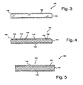
- the conductive ground plane member 102 can be disposed on a surface 106 of a substantially planar dielectric element 104. Further, a second conductive ground plane member 138 can be disposed on a second surface of the substantially planar dielectric element 104 opposed from the first side. The second conductive ground plane member can act as a reflector for the antenna.
- the conductive ground plane member 102 can be formed of any suitable conductive material.
- the conductive material can be a metal selected from the group consisting of copper, brass, aluminum, gold, or silver.
- the conductive ground plane can be formed from an alloy of these metals. Further still, the conductive ground plane can be formed from one or more of these metals plated with another metal.
- the planar dielectric element 104 can be comprised of any suitable dielectric substrate material.
- Materials commonly used for this purpose include commercially available low and high temperature cofired ceramics (LTCC, HTCC).
- LTCC low temperature cofire Green Tape TM from Dupont ® is Au and Ag compatible, has a acceptable mechanical properties with regard to thermal coefficient of expansion (TCE). Similar products are available from other manufacturers.
- LTCC substrate systems commonly combine many thin layers of ceramic and conductors.
- the individual layers are typically formed from a ceramic/glass frit that can be held together with a binder and formed into a sheet.
- Conductors can be screened onto the layers of tape to form RF antenna elements and ground planes 102, 138 as described herein. Two or more layers of the same type of tape is then fired in an oven.
- dielectric substrates include Teflon ® PTFE (PolyTetraFluoroEthylene) composites of glass fiber, woven glass and ceramics. Such products are commercially available from a variety of manufacturers. For example, Rogers Corporation of Chandler, Arizona offers such products under the trade name RT/duroid including product numbers 5880, 6002, and 6010LM. Unlike LTCC materials, these types of substrates do not generally require a firing step before they can be used. Instead, they are typically provided in the form of rigid board material with a conductive metal ground plane formed on one or both sides. Consequently, the conductive ground plane member can be etched using conventional photolithographic techniques to form the outline of the conductive ground plane 102 and the various apertures 108, 118, 120.
- Teflon ® PTFE PolyTetraFluoroEthylene
- the antenna feed connections are on opposing sides of the narrowed region 115.
- a coaxial cable (not shown) can be used for this purpose.
- An inner conductor of the coaxial cable can form an electrical connection with the conductive ground plane at channel edge 114.
- a shield portion of the coaxial cable can form an electrical connection with the conductive ground plane at channel edge 116.
- Conventional soldering techniques can be used for this purpose.
- Other types of feed arrangements are also possible as will be appreciated by those skilled in the art.
- a coupled microstrip feed, or a coupled parallel waveguide (CPW) feed could also be used for this purpose.
- CPW coupled parallel waveguide
- the patch antenna 100 disclosed in FIGS. 1-5 is a significant improvement as compared to conventional bowtie/slot antenna designs.
- the second and third apertures 118, 120 define two additional slits as compared to conventional bow-tie antennas. As shown in FIGS. 1-5 , a length of these slits can run generally transverse to opposing tapered edges 122, 124, 126, 128 and generally in parallel alignment to the transverse edges 123, 127.
- Second and third apertures 118, 120 provide reactive loading along the peripheral portion of antenna 100 along transverse edges 123, 127.
- the second and third apertures also provide a mechanism for effectively disrupting the phasing of surface currents.
- the loading technique associated with the use of the second and third apertures 118, 120 will reduce the physical size of the rectangular conductive ground plane member 102 as compared to the normal rectangular microstrip patch while operating at the same frequency.
- the peak gain is located on boresight for both frequency bands of operation and is of similar peak value.
- a gain of the antenna within the fundamental frequency band can be within about 3dB of a second gain at the first harmonic frequency band at each antenna azimuth angle, within a predetermined range of angles around antenna boresight.
- the patch antenna 100 also provides the same polarization on the fundamental frequency band and the first harmonic frequency band.
- the addition of the second and third aperture 118, 120 running perpendicular to the opposing tapered 122, 124, 126, 128 is the mechanism that results in a reduction of the physical dimensions of the conductive ground plane 102 at the fundamental frequency.
- the size reduction occurs due to increased electrical length along the resonant dimension L1.
- the second and third apertures 118, 120 also have the benefit of disrupting surface currents so that the phasing at the first harmonic frequency band f 1 will add in phase along boresight instead of at an arbitrary elevation angle. This improvement centers the peak radiation of both frequency bands on boresight.
- the second and third apertures increase the cross polarization discrimination by approximately 8 dB at the first harmonic frequency f 1 .
- the patch antenna 100 is operable on two separate frequency bands. Stated differently, this means that the patch antenna 100 can have a first electrical resonant frequency characteristic at the fundamental frequency band and a second electrical resonant frequency characteristic at the first harmonic frequency band.
- the first and second electrical resonant frequency characteristic can include an input feed point return loss magnitude greater than about 10 dB on each of the two frequency bands.
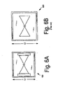
- L1 is a resonant dimension of the patch antenna 100 that is useful for drawing size comparisons of patch antenna 100 as compared to the prior art.
- the value L1 is approximately 0.28 ⁇ at an operating frequency f 0 .
- the dimension of L2 for the conventional bow-tie antenna 600 in FIG. 6b which is designed for operating at the same frequency would be about .32, or about 13% larger.
- the corresponding dimension would be approximately 0.4 ⁇ , or about 43% larger.
- the patch antenna 100 provides a significant size reduction as compared to conventional antenna designs.
- FIGS. 7-9 are a set of plots generated by computer model.
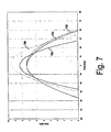
- FIG. 7 shows a set of four plots that include peak gain for a slit loaded tapered slot antenna to a conventional bow-tie slot patch antenna on a fundamental frequency and a first harmonic frequency.
- Plot 702 shows the gain characteristics of a conventional bow-tie slot antenna at a fundamental frequency f 0 .
- plot 704 shows the gain characteristic for the patch antenna 100 at the same fundamental frequency. It may be noted that the gain characteristics of the two antennas are nearly identical at this frequency.
- Plot 706 shows the gain characteristics of a conventional bow-tie slot antenna at a first harmonic f 1 of the fundamental frequency f 0 .
- Plot 708 shows the gain characteristics of patch antenna 100 at the first harmonic f 1 . It may be noted that the gain characteristics for the two antennas are similar, with the patch antenna 100 exhibiting a decrease in peak gain of only about 1.2 dB.
- Fig. 8 is a set of plots comparing cross-polarization for patch antenna 100 and a conventional bow-tie slot antenna on a fundamental frequency f 0 and a first harmonic frequency f 1 .
- Plot 802 shows the cross-polarization characteristics of a conventional bow-tie slot antenna at a fundamental frequency f 0 .
- Plot 804 shows the cross-polarization characteristics of the patch antenna 100 at the same fundamental frequency f 0 .
- Plot 806 shows the cross-polarization characteristics of a conventional bow-tie slot antenna at the first harmonic frequency f 1 .
- Plot 808 shows the cross-polarization characteristic of the patch antenna 100 at the first harmonic frequency f 1 .
- the patch antenna 100 exhibits improved cross-polarization characteristics at the fundamental frequency f 0 in and around boresight. At the first harmonic frequency f 1 , there is a further improvement in cross-polarization levels with the patch antenna 100.
- peak cross-polarization shown by plot 808 is as much as 8 dB lower as compared to peak cross-polarization values for plot the conventional bow-tie antenna shown in plot 806.
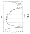
- Fig. 9 is a set of plots showing return loss versus frequency for a slit loaded tapered slot antenna and a conventional bow-tie slot patch antenna. Return loss of the conventional bow-tie slot patch antenna is shown in plot 902. Return loss for the patch antenna 100 is show in plot 904. The return loss for the patch antenna 100 is degraded slightly at the fundamental frequency f 0 as compared to the conventional bow-tie antenna. However, the return loss improves somewhat with the antenna 100 at the first harmonic frequency f 1 .
- FIG. 10 there is shown a diagram of a slit-loaded bow tie slot antenna diagram that is useful for understanding the invention.
- the diagram in Fig. 10 shows one possible set of dimensions that can be used in connection with the invention.
- the plots shown in Figs. 7 - 10 were produced with a slit-loaded bow tie slot antenna having dimensions consistent with those shown in Fig. 10 .
- the dimensions below are expressed in fractions of a wavelength at a resonant frequency of the device.
Landscapes
- Waveguide Aerials (AREA)
Claims (9)
- Patch-Antenne für eine drahtlose Kommunikationsvorrichtung, aufweisend:ein leitfähiges Masseplattenelement (102);eine erste Öffnung (108), die in dem leitfähigen Masseplattenelement vorgesehen ist, umfassend einen ersten sich verjüngenden Bereich und einen zweiten sich verjüngenden Bereich, wobei der erste und der zweite sich verjüngende Bereich jeweils gegenüberliegende sich verjüngende Kanten aufweisen, die entlang einer Richtung zu einer Mittelachse der ersten Öffnung hin konvergieren, und eine erste Querkante, welche die gegenüberliegenden sich verjüngenden Kanten des ersten sich verjüngenden Bereichs an einem von der Mittelachse distalen Punkt verbinden, und eine zweite Querkante, welche die gegenüberliegenden sich verjüngenden Kanten des zweiten sich verjüngenden Bereichs an einem von der Mittelachse distalen Punkt verbinden, so dass sie eine Form eines Bow-Tie definieren; dadurch gekennzeichnet, dasseine zweite, längliche Öffnung (118) in der leitfähigen Masseplatte ausgebildet ist, wobei eine längliche Kante der zweiten, länglichen Öffnung benachbart zu und in paralleler Ausrichtung zu der ersten Querkante und durch eine Lücke, die durch einen Bereich der leitfähigen Masseplatte definiert ist, getrennt von der ersten Querkante positioniert ist; undeine dritte, längliche Öffnung (120) in der leitfähigen Masseplatte ausgebildet ist, wobei eine längliche Kante der dritten, länglichen Öffnung benachbart zu und in paralleler Ausrichtung zu der ersten Querkante und durch eine Lücke, die durch einen Bereich der leitfähigen Masseplatte definiert ist, getrennt von der zweiten Querkante positioniert ist.
- Patch-Antenne nach Anspruch 1, bei der das leitfähige Masseplattenelement eine im Wesentlichen rechteckige Form aufweist.
- Patch-Antenne nach Anspruch 2, bei der die rechteckige Form eine resonante Dimension (L1) aufweist, welche eine Resonanzfrequenzeigenschaft der Antenne bestimmt.
- Patch-Antenne nach Anspruch 1, bei der die zweite, längliche Öffnung eine im Wesentlichen rechteckige Form aufweist.
- Patch-Antenne nach Anspruch 1, bei der das leitfähige Masseplattenelement an einer ersten Seite eines im Wesentlichen planaren dielektrischen Elements angeordnet ist.
- Patch-Antenne nach Anspruch 5, bei der das zweite leitfähige Masseplattenelement an einer zweiten Seite eines im Wesentlichen planaren dielektrischen Elements gegenüber der ersten Seite angeordnet ist.
- Patch-Antenne nach Anspruch 1, bei der die erste Öffnung ferner einen verschmälerten Bereich umfasst, der sich zwischen dem ersten und dem zweiten sich verjüngenden Bereich erstreckt.
- Patch-Antenne nach Anspruch 1, bei welcher der verschmälerte Bereich gegenüberliegenden Kanalkanten aufweist, die zusammen einen Funkfrequenzspeisungspunkt für die Patch-Antenne definieren.
- Patch-Antenne nach Anspruch 1, bei der die Antenne eine erste elektrische Resonanzfrequenzeigenschaft auf einem Grundfrequenzband und eine zweite elektrische Resonanzfrequenzeigenschaft auf einer ersten Oberwelle des Grundfrequenzbands aufweist.
Applications Claiming Priority (2)
| Application Number | Priority Date | Filing Date | Title |
|---|---|---|---|
| US11/358,146 US7372409B2 (en) | 2006-02-21 | 2006-02-21 | Slit loaded tapered slot patch antenna |
| PCT/US2007/002345 WO2007097882A2 (en) | 2006-02-21 | 2007-01-30 | Slit loaded tapered slot patch antenna |
Publications (3)
| Publication Number | Publication Date |
|---|---|
| EP1992043A2 EP1992043A2 (de) | 2008-11-19 |
| EP1992043A4 EP1992043A4 (de) | 2010-12-01 |
| EP1992043B1 true EP1992043B1 (de) | 2012-03-28 |
Family
ID=38427649
Family Applications (1)
| Application Number | Title | Priority Date | Filing Date |
|---|---|---|---|
| EP07749408A Expired - Fee Related EP1992043B1 (de) | 2006-02-21 | 2007-01-30 | Schlitzgeladene patchantenne mit konischem schlitz |
Country Status (6)
| Country | Link |
|---|---|
| US (1) | US7372409B2 (de) |
| EP (1) | EP1992043B1 (de) |
| JP (1) | JP2009527985A (de) |
| CA (1) | CA2643166C (de) |
| TW (1) | TWI327789B (de) |
| WO (1) | WO2007097882A2 (de) |
Cited By (1)
| Publication number | Priority date | Publication date | Assignee | Title |
|---|---|---|---|---|
| TWI506859B (zh) * | 2013-11-08 | 2015-11-01 | Nat Univ Chin Yi Technology | 應用於2g、3g和4g系統之共平面波導饋入天線 |
Families Citing this family (36)
| Publication number | Priority date | Publication date | Assignee | Title |
|---|---|---|---|---|
| USD347612S (en) * | 1991-05-20 | 1994-06-07 | Allen Dillis V | Steering wheel assembly with communication keyboard |
| US7522114B2 (en) * | 2005-02-09 | 2009-04-21 | Pinyon Technologies, Inc. | High gain steerable phased-array antenna |
| PL2126799T3 (pl) * | 2007-03-23 | 2018-10-31 | Zih Corp. | Etykieta rfid o zmniejszonym rozstrajaniu |
| US7923688B2 (en) * | 2007-10-31 | 2011-04-12 | Raytheon Company | Multiple-band detector using frequency selective slots |
| US7821462B1 (en) * | 2008-07-28 | 2010-10-26 | Itt Manufacturing Enterprises, Inc. | Compact, dual-polar broadband monopole |
| US8053734B2 (en) * | 2009-04-30 | 2011-11-08 | Raytehon Company | Nano-antenna for wideband coherent conformal IR detector arrays |
| US7923689B2 (en) * | 2009-04-30 | 2011-04-12 | Raytheon Company | Multi-band sub-wavelength IR detector having frequency selective slots and method of making the same |
| US20100289701A1 (en) * | 2009-05-15 | 2010-11-18 | Microsoft Corporation | Antenna configured for bandwidth improvement on a small substrate. |
| US8514136B2 (en) * | 2009-10-26 | 2013-08-20 | The Boeing Company | Conformal high frequency antenna |
| JP5731745B2 (ja) * | 2009-10-30 | 2015-06-10 | 古野電気株式会社 | アンテナ装置およびレーダ装置 |
| US8754822B1 (en) * | 2010-08-17 | 2014-06-17 | Amazon Technologies, Inc. | Tuning elements for specific absorption rate reduction |
| USD695277S1 (en) * | 2011-04-25 | 2013-12-10 | ChamTech Technologies, Incorporated | Antenna |
| USD652409S1 (en) * | 2011-04-25 | 2012-01-17 | ChamTech Technologies, Incorporated | Antenna |
| TWI459302B (zh) * | 2011-12-26 | 2014-11-01 | China Steel Corp | Variable operation frequency of the RFID tag |
| JP2014131231A (ja) * | 2012-12-28 | 2014-07-10 | Maspro Denkoh Corp | アンテナ放射器 |
| US9450647B2 (en) * | 2013-06-10 | 2016-09-20 | Intel Corporation | Antenna coupler for near field wireless docking |
| US9397393B2 (en) | 2013-07-22 | 2016-07-19 | Blackberry Limited | Method and system for multiple feed point antennas |
| CN103779654B (zh) * | 2014-01-14 | 2016-02-03 | 西安电子科技大学 | 一种采用自相似馈电技术的双频宽带领结天线 |
| US9899741B2 (en) * | 2015-01-26 | 2018-02-20 | Rodradar Ltd. | Radio frequency antenna |
| US10199745B2 (en) | 2015-06-04 | 2019-02-05 | The Boeing Company | Omnidirectional antenna system |
| US10158180B1 (en) | 2015-08-05 | 2018-12-18 | Northrop Grumman Systems Corporation | Ultrawideband nested bowtie array |
| USD795228S1 (en) * | 2016-03-04 | 2017-08-22 | Airgain Incorporated | Antenna |
| USD795847S1 (en) * | 2016-03-08 | 2017-08-29 | Airgain Incorporated | Antenna |
| RU2622488C1 (ru) * | 2016-04-06 | 2017-06-15 | Самсунг Электроникс Ко., Лтд. | Антенна подповерхностного зондирования |
| US10096892B2 (en) | 2016-08-30 | 2018-10-09 | The Boeing Company | Broadband stacked multi-spiral antenna array integrated into an aircraft structural element |
| US11289814B2 (en) | 2017-11-10 | 2022-03-29 | Raytheon Company | Spiral antenna and related fabrication techniques |
| KR102545915B1 (ko) * | 2017-11-10 | 2023-06-22 | 레이던 컴퍼니 | 적층 제조 기술(amt) 저 프로파일 라디에이터 |
| IL275262B2 (en) | 2018-02-28 | 2024-09-01 | Raytheon Co | Additive manufacturing technology (amt) low profile signal divider |
| USD924210S1 (en) * | 2018-05-11 | 2021-07-06 | Skyworks Solutions, Inc. | Antenna |
| NL2022823B1 (en) * | 2019-03-27 | 2020-10-02 | The Antenna Company International N V | Dual-band directional antenna, wireless device, and wireless communication system |
| CN109921181B (zh) * | 2019-04-10 | 2024-05-14 | 西南交通大学 | 一种双层蝶形天线 |
| CN110233325B (zh) * | 2019-05-27 | 2021-07-16 | 国网新疆电力有限公司电力科学研究院 | 蝶形偶极子缝隙天线基板制造方法及蝶形偶极子缝隙天线 |
| CN112467351B (zh) * | 2020-11-19 | 2022-04-19 | 中国电子科技集团公司第二十九研究所 | 一种多谐振激励背腔天线 |
| CN112490655B (zh) * | 2020-11-20 | 2023-06-06 | 榆林学院 | 一种多频双层介质板馈源贴片与辐射缝隙互补微带天线 |
| CN112751172B (zh) * | 2020-12-25 | 2021-10-22 | 电子科技大学 | 一种用于射频能量采集的高增益定向辐射双频接收天线 |
| CN115603044A (zh) * | 2022-10-21 | 2023-01-13 | 网络通信与安全紫金山实验室(Cn) | 微带贴片天线 |
Family Cites Families (12)
| Publication number | Priority date | Publication date | Assignee | Title |
|---|---|---|---|---|
| JP3004082B2 (ja) * | 1991-06-19 | 2000-01-31 | 京セラ株式会社 | 平板型スロットアンテナ |
| US6424309B1 (en) * | 2000-02-18 | 2002-07-23 | Telecommunications Research Laboratories | Broadband compact slot dipole/monopole and electric dipole/monopole combined antenna |
| DE10049845A1 (de) * | 2000-10-09 | 2002-04-11 | Philips Corp Intellectual Pty | Mehrband-Mikrowellenantenne |
| US6429819B1 (en) * | 2001-04-06 | 2002-08-06 | Tyco Electronics Logistics Ag | Dual band patch bowtie slot antenna structure |
| US6421018B1 (en) * | 2001-05-31 | 2002-07-16 | Andrew Corporation | Bowtie inductive coupler |
| JP2003078345A (ja) * | 2001-09-03 | 2003-03-14 | Sansei Denki Kk | スロット型ボウタイアンテナ装置、および同構成方法 |
| KR100467904B1 (ko) * | 2001-12-04 | 2005-01-26 | 주식회사 에이스테크놀로지 | 스켈톤 슬롯 복사기 및 그를 이용한 다중대역 패치 안테나 |
| US6762730B2 (en) * | 2002-10-04 | 2004-07-13 | Spx Corporation | Crossed bow tie slot antenna |
| JP4054270B2 (ja) * | 2003-03-24 | 2008-02-27 | 峰光電子株式会社 | デュアルバンドスロットボウタイアンテナ、及び、その構成方法 |
| KR100996092B1 (ko) * | 2003-12-31 | 2010-11-22 | 삼성전자주식회사 | 주파수 노치 기능을 가지는 평면형 초광대역 안테나 |
| JP4548281B2 (ja) * | 2005-08-31 | 2010-09-22 | 日立電線株式会社 | 広帯域アンテナ |
| US7388550B2 (en) * | 2005-10-11 | 2008-06-17 | Tdk Corporation | PxM antenna with improved radiation characteristics over a broad frequency range |
-
2006
- 2006-02-21 US US11/358,146 patent/US7372409B2/en active Active
-
2007
- 2007-01-30 JP JP2008556332A patent/JP2009527985A/ja active Pending
- 2007-01-30 WO PCT/US2007/002345 patent/WO2007097882A2/en not_active Ceased
- 2007-01-30 EP EP07749408A patent/EP1992043B1/de not_active Expired - Fee Related
- 2007-01-30 CA CA2643166A patent/CA2643166C/en not_active Expired - Fee Related
- 2007-02-08 TW TW096104625A patent/TWI327789B/zh not_active IP Right Cessation
Cited By (1)
| Publication number | Priority date | Publication date | Assignee | Title |
|---|---|---|---|---|
| TWI506859B (zh) * | 2013-11-08 | 2015-11-01 | Nat Univ Chin Yi Technology | 應用於2g、3g和4g系統之共平面波導饋入天線 |
Also Published As
| Publication number | Publication date |
|---|---|
| US20070194999A1 (en) | 2007-08-23 |
| TWI327789B (en) | 2010-07-21 |
| CA2643166A1 (en) | 2007-08-30 |
| US7372409B2 (en) | 2008-05-13 |
| JP2009527985A (ja) | 2009-07-30 |
| EP1992043A2 (de) | 2008-11-19 |
| WO2007097882A3 (en) | 2009-01-15 |
| WO2007097882A2 (en) | 2007-08-30 |
| EP1992043A4 (de) | 2010-12-01 |
| CA2643166C (en) | 2012-05-29 |
| TW200746545A (en) | 2007-12-16 |
Similar Documents
| Publication | Publication Date | Title |
|---|---|---|
| CA2643166C (en) | Slit loaded tapered slot patch antenna | |
| US5828340A (en) | Wideband sub-wavelength antenna | |
| US6043785A (en) | Broadband fixed-radius slot antenna arrangement | |
| Liang et al. | Study of CPW-fed circular disc monopole antenna for ultra wideband applications | |
| US5990849A (en) | Compact spiral antenna | |
| US4847625A (en) | Wideband, aperture-coupled microstrip antenna | |
| US6429819B1 (en) | Dual band patch bowtie slot antenna structure | |
| US7605769B2 (en) | Multi-ban U-slot antenna | |
| Liu | Wideband dual-frequency double inverted-L CPW-fed monopole antenna for WLAN application | |
| Alibakhshikenari et al. | High-Performance 50µm silicon-based On-chip antenna with high port-to-port isolation implemented by metamaterial and SIW concepts for THz integrated systems | |
| KR20050107881A (ko) | 광대역 특성의 다중 미앤더 스트립 모노폴 안테나 | |
| US20050237244A1 (en) | Compact RF antenna | |
| CN210074169U (zh) | 一种基于接地共面波导的矩形微带串馈天线 | |
| Lee et al. | A wideband planar monopole antenna array with circular polarized and band-notched characteristics | |
| KR102123976B1 (ko) | 일차원 전자기 밴드갭 접지 구조를 구비하는 안테나 장치 | |
| Hamid et al. | Wideband reconfigurable log periodic patch array | |
| CN109786985B (zh) | 一种基于接地共面波导的矩形微带串馈天线 | |
| Jhuang et al. | Design of compact microstrip dual‐band bandpass filters with λ/4 stepped‐impedance resonators | |
| IL279008B1 (en) | End-fire tapered slot antenna | |
| CN115244781B (zh) | 天线和天线阵列 | |
| Ho et al. | Design of balanced wideband filtering circularly polarized antenna using quasi-self-complementary structure | |
| CN112821058B (zh) | 一种Vivaldi天线 | |
| JP7216263B2 (ja) | アンテナ装置および携帯端末 | |
| Islam et al. | Small multi-band microstrip antenna for wireless applications | |
| KR102508317B1 (ko) | 이동통신 단말기용 폴디드 패치 안테나 |
Legal Events
| Date | Code | Title | Description |
|---|---|---|---|
| PUAI | Public reference made under article 153(3) epc to a published international application that has entered the european phase |
Free format text: ORIGINAL CODE: 0009012 |
|
| 17P | Request for examination filed |
Effective date: 20080916 |
|
| AK | Designated contracting states |
Kind code of ref document: A2 Designated state(s): AT BE BG CH CY CZ DE DK EE ES FI FR GB GR HU IE IS IT LI LT LU LV MC NL PL PT RO SE SI SK TR |
|
| AX | Request for extension of the european patent |
Extension state: AL BA HR MK RS |
|
| R17D | Deferred search report published (corrected) |
Effective date: 20090115 |
|
| DAX | Request for extension of the european patent (deleted) | ||
| RBV | Designated contracting states (corrected) |
Designated state(s): DE FR GB |
|
| A4 | Supplementary search report drawn up and despatched |
Effective date: 20101104 |
|
| GRAP | Despatch of communication of intention to grant a patent |
Free format text: ORIGINAL CODE: EPIDOSNIGR1 |
|
| RIC1 | Information provided on ipc code assigned before grant |
Ipc: H01Q 13/10 20060101AFI20110722BHEP |
|
| GRAS | Grant fee paid |
Free format text: ORIGINAL CODE: EPIDOSNIGR3 |
|
| GRAA | (expected) grant |
Free format text: ORIGINAL CODE: 0009210 |
|
| AK | Designated contracting states |
Kind code of ref document: B1 Designated state(s): DE FR GB |
|
| REG | Reference to a national code |
Ref country code: GB Ref legal event code: FG4D |
|
| REG | Reference to a national code |
Ref country code: DE Ref legal event code: R096 Ref document number: 602007021628 Country of ref document: DE Effective date: 20120524 |
|
| PLBE | No opposition filed within time limit |
Free format text: ORIGINAL CODE: 0009261 |
|
| STAA | Information on the status of an ep patent application or granted ep patent |
Free format text: STATUS: NO OPPOSITION FILED WITHIN TIME LIMIT |
|
| 26N | No opposition filed |
Effective date: 20130103 |
|
| REG | Reference to a national code |
Ref country code: DE Ref legal event code: R097 Ref document number: 602007021628 Country of ref document: DE Effective date: 20130103 |
|
| PGFP | Annual fee paid to national office [announced via postgrant information from national office to epo] |
Ref country code: DE Payment date: 20130129 Year of fee payment: 7 Ref country code: FR Payment date: 20130211 Year of fee payment: 7 Ref country code: GB Payment date: 20130125 Year of fee payment: 7 |
|
| REG | Reference to a national code |
Ref country code: DE Ref legal event code: R119 Ref document number: 602007021628 Country of ref document: DE |
|
| GBPC | Gb: european patent ceased through non-payment of renewal fee |
Effective date: 20140130 |
|
| REG | Reference to a national code |
Ref country code: DE Ref legal event code: R119 Ref document number: 602007021628 Country of ref document: DE Effective date: 20140801 |
|
| PG25 | Lapsed in a contracting state [announced via postgrant information from national office to epo] |
Ref country code: DE Free format text: LAPSE BECAUSE OF NON-PAYMENT OF DUE FEES Effective date: 20140801 |
|
| REG | Reference to a national code |
Ref country code: FR Ref legal event code: ST Effective date: 20140930 |
|
| PG25 | Lapsed in a contracting state [announced via postgrant information from national office to epo] |
Ref country code: FR Free format text: LAPSE BECAUSE OF NON-PAYMENT OF DUE FEES Effective date: 20140131 Ref country code: GB Free format text: LAPSE BECAUSE OF NON-PAYMENT OF DUE FEES Effective date: 20140130 |