EP1993948B1 - Dispositif mems - Google Patents
Dispositif mems Download PDFInfo
- Publication number
- EP1993948B1 EP1993948B1 EP07705267.8A EP07705267A EP1993948B1 EP 1993948 B1 EP1993948 B1 EP 1993948B1 EP 07705267 A EP07705267 A EP 07705267A EP 1993948 B1 EP1993948 B1 EP 1993948B1
- Authority
- EP
- European Patent Office
- Prior art keywords
- substrate
- sacrificial layer
- layer
- membrane
- electronic circuit
- Prior art date
- Legal status (The legal status is an assumption and is not a legal conclusion. Google has not performed a legal analysis and makes no representation as to the accuracy of the status listed.)
- Not-in-force
Links
Images




Classifications
-
- B—PERFORMING OPERATIONS; TRANSPORTING
- B81—MICROSTRUCTURAL TECHNOLOGY
- B81C—PROCESSES OR APPARATUS SPECIALLY ADAPTED FOR THE MANUFACTURE OR TREATMENT OF MICROSTRUCTURAL DEVICES OR SYSTEMS
- B81C1/00—Manufacture or treatment of devices or systems in or on a substrate
- B81C1/00015—Manufacture or treatment of devices or systems in or on a substrate for manufacturing microsystems
- B81C1/00134—Manufacture or treatment of devices or systems in or on a substrate for manufacturing microsystems comprising flexible or deformable structures
- B81C1/00158—Diaphragms, membranes
-
- B—PERFORMING OPERATIONS; TRANSPORTING
- B81—MICROSTRUCTURAL TECHNOLOGY
- B81B—MICROSTRUCTURAL DEVICES OR SYSTEMS, e.g. MICROMECHANICAL DEVICES
- B81B3/00—Devices comprising flexible or deformable elements, e.g. comprising elastic tongues or membranes
- B81B3/0018—Structures acting upon the moving or flexible element for transforming energy into mechanical movement or vice versa, i.e. actuators, sensors, generators
- B81B3/0027—Structures for transforming mechanical energy, e.g. potential energy of a spring into translation, sound into translation
-
- B—PERFORMING OPERATIONS; TRANSPORTING
- B81—MICROSTRUCTURAL TECHNOLOGY
- B81C—PROCESSES OR APPARATUS SPECIALLY ADAPTED FOR THE MANUFACTURE OR TREATMENT OF MICROSTRUCTURAL DEVICES OR SYSTEMS
- B81C1/00—Manufacture or treatment of devices or systems in or on a substrate
- B81C1/00015—Manufacture or treatment of devices or systems in or on a substrate for manufacturing microsystems
- B81C1/00222—Integrating an electronic processing unit with a micromechanical structure
- B81C1/00246—Monolithic integration, i.e. micromechanical structure and electronic processing unit are integrated on the same substrate
-
- B—PERFORMING OPERATIONS; TRANSPORTING
- B81—MICROSTRUCTURAL TECHNOLOGY
- B81C—PROCESSES OR APPARATUS SPECIALLY ADAPTED FOR THE MANUFACTURE OR TREATMENT OF MICROSTRUCTURAL DEVICES OR SYSTEMS
- B81C1/00—Manufacture or treatment of devices or systems in or on a substrate
- B81C1/00865—Multistep processes for the separation of wafers into individual elements
-
- B—PERFORMING OPERATIONS; TRANSPORTING
- B81—MICROSTRUCTURAL TECHNOLOGY
- B81C—PROCESSES OR APPARATUS SPECIALLY ADAPTED FOR THE MANUFACTURE OR TREATMENT OF MICROSTRUCTURAL DEVICES OR SYSTEMS
- B81C1/00—Manufacture or treatment of devices or systems in or on a substrate
- B81C1/00865—Multistep processes for the separation of wafers into individual elements
- B81C1/00904—Multistep processes for the separation of wafers into individual elements not provided for in groups B81C1/00873 - B81C1/00896
-
- G—PHYSICS
- G01—MEASURING; TESTING
- G01L—MEASURING FORCE, STRESS, TORQUE, WORK, MECHANICAL POWER, MECHANICAL EFFICIENCY, OR FLUID PRESSURE
- G01L9/00—Measuring steady of quasi-steady pressure of fluid or fluent solid material by electric or magnetic pressure-sensitive elements; Transmitting or indicating the displacement of mechanical pressure-sensitive elements, used to measure the steady or quasi-steady pressure of a fluid or fluent solid material, by electric or magnetic means
- G01L9/0041—Transmitting or indicating the displacement of flexible diaphragms
- G01L9/0072—Transmitting or indicating the displacement of flexible diaphragms using variations in capacitance
- G01L9/0073—Transmitting or indicating the displacement of flexible diaphragms using variations in capacitance using a semiconductive diaphragm
-
- H—ELECTRICITY
- H04—ELECTRIC COMMUNICATION TECHNIQUE
- H04R—LOUDSPEAKERS, MICROPHONES, GRAMOPHONE PICK-UPS OR LIKE ACOUSTIC ELECTROMECHANICAL TRANSDUCERS; ELECTRIC HEARING AIDS; PUBLIC ADDRESS SYSTEMS
- H04R19/00—Electrostatic transducers
- H04R19/005—Electrostatic transducers using semiconductor materials
-
- H—ELECTRICITY
- H04—ELECTRIC COMMUNICATION TECHNIQUE
- H04R—LOUDSPEAKERS, MICROPHONES, GRAMOPHONE PICK-UPS OR LIKE ACOUSTIC ELECTROMECHANICAL TRANSDUCERS; ELECTRIC HEARING AIDS; PUBLIC ADDRESS SYSTEMS
- H04R19/00—Electrostatic transducers
- H04R19/04—Microphones
-
- H—ELECTRICITY
- H04—ELECTRIC COMMUNICATION TECHNIQUE
- H04R—LOUDSPEAKERS, MICROPHONES, GRAMOPHONE PICK-UPS OR LIKE ACOUSTIC ELECTROMECHANICAL TRANSDUCERS; ELECTRIC HEARING AIDS; PUBLIC ADDRESS SYSTEMS
- H04R3/00—Circuits for transducers
- H04R3/005—Circuits for transducers for combining the signals of two or more microphones
-
- B—PERFORMING OPERATIONS; TRANSPORTING
- B81—MICROSTRUCTURAL TECHNOLOGY
- B81B—MICROSTRUCTURAL DEVICES OR SYSTEMS, e.g. MICROMECHANICAL DEVICES
- B81B2201/00—Specific applications of microelectromechanical systems
- B81B2201/02—Sensors
- B81B2201/0257—Microphones or microspeakers
-
- B—PERFORMING OPERATIONS; TRANSPORTING
- B81—MICROSTRUCTURAL TECHNOLOGY
- B81B—MICROSTRUCTURAL DEVICES OR SYSTEMS, e.g. MICROMECHANICAL DEVICES
- B81B2201/00—Specific applications of microelectromechanical systems
- B81B2201/02—Sensors
- B81B2201/0264—Pressure sensors
-
- B—PERFORMING OPERATIONS; TRANSPORTING
- B81—MICROSTRUCTURAL TECHNOLOGY
- B81B—MICROSTRUCTURAL DEVICES OR SYSTEMS, e.g. MICROMECHANICAL DEVICES
- B81B2201/00—Specific applications of microelectromechanical systems
- B81B2201/02—Sensors
- B81B2201/0292—Sensors not provided for in B81B2201/0207 - B81B2201/0285
-
- B—PERFORMING OPERATIONS; TRANSPORTING
- B81—MICROSTRUCTURAL TECHNOLOGY
- B81C—PROCESSES OR APPARATUS SPECIALLY ADAPTED FOR THE MANUFACTURE OR TREATMENT OF MICROSTRUCTURAL DEVICES OR SYSTEMS
- B81C2201/00—Manufacture or treatment of microstructural devices or systems
- B81C2201/05—Temporary protection of devices or parts of the devices during manufacturing
- B81C2201/056—Releasing structures at the end of the manufacturing process
Definitions
- This invention relates to MEMS devices.
- MEMS Micro electrical mechanical systems
- these devices are, for example, pressure sensors, ultrasonic transducers and microphones.
- these devices comprise one or more membranes with electrodes for read-out/drive deposited on the membranes and/or a substrate.
- the read out is usually accomplished by measuring the capacitance between the electrodes.
- the device is driven by an applying a potential difference across the electrodes.
- the membranes are manufactured using a sacrificial layer, which is typically SiO 2 . This is removed later in the process to leave the membrane suspended and free to move.
- the membranes are thin, of the order microns, and can range in size from tens to thousands of microns. As a result, the devices can be fragile and may be damaged during singulation.
- Singulation is a process in which a substrate wafer on which the MEMS devices are fabricated is diced up so that only one device (or a group of devices) is found on each diced piece. This process is typically achieved by dicing the wafer with a high-speed rotating diamond blade. Alternatively the wafer may be cut up using a laser, or scribed and cleaved along a crystallographic axis. All of these dicing methods have associated problems when applied to MEMS structures.
- a lubricating coolant usually water
- water that is meant to prevent the temperature of the wafer from becoming too high and to ensure the diamond blade stays in a safe operating range.
- a lubricating coolant usually water
- the lubricating coolant may be sprayed onto the wafer at high speed thus placing any delicate sensor structure under high mechanical stress and potentially damaging it.
- Laser singulation is slightly cleaner than blade dicing but is more expensive. However, the heating produced by the cutting process may set up thermal gradients leading to areas of different thermal expansion in the sensor structures that may distort them and render them useless. Also the laser singulation process produces some residue that may clog any open structure and prevent the device from operating properly.
- singulating the wafer by scribing and cleaving places extremely high mechanical stress on the wafer during the cleaving process and produces a large amount of debris that may damage the device as above.
- WO 01/14248 identifies these issues for silicon microphones.
- the devices are diced and then mounted/attached on a substrate carrier using a chemically resistant adhesive before the sacrificial layer is removed.
- the sensor is then subjected to a chemical etching process, for example by using hydrofluoric acid, to remove the sacrificial layer.
- CMOS complementary-metal-oxide-semiconductor
- US 2005/0266599 describes a fabrication method for MEMS devices, for example accelerometers.
- a substrate having a sacrificial layer sandwiched between two semiconductor layers i.e. a silicon-on-insulator (SOI) wafer is envisaged.
- SOI silicon-on-insulator
- the wafer is micro machined but leaving all or part of the sacrificial layer in place.
- the wafer is attached to an adhesive sheet and diced.
- the sacrificial SiO 2 layer is subsequently removed using a chemical etch.
- Use of the two semiconductor layer substrate with sandwiched oxide layer precludes its application to CMOS processes.
- WO 03/053844 US5,061,049 and WO 99/03146 are other examples of known fabrication techniques for MEMS devices.
- This invention provides a method of fabricating a micro-electrical-mechanical system (MEMS) apparatus on a substrate, the method comprising the steps of: processing the substrate so as to fabricate an electronic circuit; depositing a first electrode that is operably coupled with the electronic circuit; depositing a membrane so that it is mechanically coupled to the first electrode; applying a sacrificial layer; depositing a structural layer and a second electrode that is operably coupled with the electronic circuit so that the sacrificial layer is disposed between the membrane and the structural layer so as to form a preliminary structure; etching the substrate (10) to create a sound port (20); attaching the substrate to a carrier using dicing tape; singulating the substrate; and removing the sacrificial layer so as to form a MEMS structure, wherein the step of singulating the substrate is carried out before the step of removing the sacrificial layer, and wherein both the singulating step and the step of removing the sacrificial layer are carried our while the substrate is still on the
- Embodiments of the present invention provide a MEMS fabrication process in which the processes and materials involved in the fabrication of the MEMS membranes are compatible with (CMOS) fabrication processes.
- CMOS complementary metal-oxide-semiconductor
- CMOS compatible process for defining membrane structures is described.
- ulation may refer to a process which results in one MEMS device per diced piece or alternatively a group of MEMS devices per diced piece.
- FIG. 1 shows a cross-sectional view of a MEMS device that may be manufactured according to an embodiment of the invention.
- the MEMS device is a capacitively coupled microphone that is operably coupled to circuit regions 11.
- the device is fabricated from a silicon substrate 10. (In this example, for integration with CMOS electronics the substrate is silicon, but it will be appreciated that other substrate materials and electronic fabrication techniques could be used instead.
- the device In order to process an electrical output signal from the microphone, the device has circuit regions 11 fabricated by standard CMOS processes on the substrate.
- the circuit regions comprise aluminium circuit interconnects 13 that are used to electrically connect to the microphone via interconnect points 14.
- a silica based insulating and protective layer 12 covers the circuit regions and the rest of the substrate.
- the microphone is formed from a suspended membrane 16 that is mechanically coupled to electrodes 15 and 17. Interposed between the electrodes is an air gap 21 to allow the membrane 16 to move freely in response to pressure differences generated by sound waves.
- a lower electrode 15 connects to one of the circuit regions 11 via one of the interconnect points 14.
- the lower electrode is mechanically coupled to the membrane 16 which is suspended across a hole 20 in the substrate 10.
- the hole 20 is in fact sealed in use by virtue of the fact that the MEMS device is mounted on a carrier, but this does not significantly impede its operation (as a hole) because the large back-volume between the membrane and such a carrier presents a low resistance and enables the lower membrane to move freely in response to differential pressure differences generated by sound waves.
- a second electrode 17 Suspended above the membrane and attached to a generally rigid structural layer or backplate 18 is a second electrode 17. This is mechanically coupled to the backplate and connected to one of the circuit regions 11 via one of the interconnect points 14. To prevent the formation of a small sealed cavity that would impede the microphone from operating correctly, vent holes 19 are arranged in the backplate 18 so as to allow free movement of air molecules.
- the membrane 16 In response to a sound wave corresponding to a longitudinal pressure wave incident on the microphone, the membrane 16 is deformed slightly from its equilibrium position. The distance between the lower electrode 15 and upper electrode 17 is correspondingly altered, giving rise to a change in capacitance between the two electrodes that is subsequently detected by the circuit regions 11.
- a CMOS silicon wafer 13 is processed to fabricate circuit regions 11 using standard processing techniques such as ion implantation, photomasking, metal deposition and etching.
- the circuit regions comprise any circuit operable to interface with a MEMS microphone.
- the circuit may be a pre-amplifier connected so as to amplify an output of the microphone.
- the circuit may contain a charge-pump to generate a bias, typically around 10 volts, across the two electrodes. This has the effect that changes in the electrode separation then change the device capacitance; assuming constant charge, the voltage on the output terminal is correspondingly changed.
- a high impedance pre-amplifier can then detect such a change in voltage.
- the circuit regions may optionally comprise an analogue-to-digital converter to convert the output of the microphone or an output of the pre-amplifier into a digital signal, and optionally a digital signal processor to process or part-process such a digital signal.
- the circuit may comprise a digital-to-analogue converter and/or a transmitter/receiver suitable for wireless communication.
- the contacts/interconnects 13 of the circuit regions 11 are typically made by sputtering aluminium.
- the contacts/interconnects are then protected from damage by further processing steps with a silica based insulating and protective layer 12.
- An etch stop layer in the form of, for example, plasma enhanced chemical vapour deposition (PECVD) deposited silicon nitride or silica is included as part of the CMOS fabrication process. (Note that the layer might not be pure silica - BoroPhosphoSilicate Glass or BPSG is a possibility as it can be deposited at lower temperatures).
- PECVD plasma enhanced chemical vapour deposition
- the upper electrode 17 and also the electrode 15 below the silicon nitride membrane 16 are aluminium.
- the electrode could be attacked by the back-hole etching process and so to protect it an etch-stop layer could be included, to be removed later in the process with a simple wet etch process following the hole etch.
- contact points are opened up in the doped silica layer by patterning with resist and dry etching through using a CF 4 /H 2 gas mix to expose the interconnect points 13 as shown in Figure 3 .
- the bottom electrode 15 is then deposited at a step s12, typically by sputtering aluminium. Alternatively, the bottom electrode 15 may be deposited during the fabrication of the circuit regions 11 at step s11. Depositing the electrode by sputtering is preferable to other methods such as thermal evaporation due to the low substrate temperatures used. This ensures compatibility with CMOS fabrication processes.
- this method benefits from the ability to accurately control the composition of the thin film that is deposited.
- Sputtering deposits material equally over all surfaces so the deposited thin film has to be patterned by resist application and dry etching with a Cl 2 /BCl 3 gas mix to define the shape of the lower electrode 15 as well as to define the interconnect points 14 that allow interconnection to the underlying CMOS circuit.
- the lower membrane 16 is then deposited at a step s13 via plasma enhanced chemical vapour deposition (PECVD) at 300°C with Silane (SiH 4 ), Ammonia (NH 3 ) and nitrogen (N 2 ) with flow rates of 40,40 and 1400 sccm (standard cubic centimetres/minute) respectively.
- PECVD plasma enhanced chemical vapour deposition
- the RF power can be 20W and can be alternated every 6 seconds between a high frequency (13.56MHz) and a low frequency (400kHz).
- a high frequency 13.56MHz
- a low frequency 400kHz.
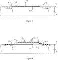
- a sacrificial layer 50 is used in the microphone manufacturing process. This layer is deposited as shown in Figure 5 and then removed at a step s19 in order to define a cavity.
- the sacrificial layer 50 can be made of a number of materials which can be removed using a dry release process. This is advantageous in that no additional process steps or drying are required after the sacrificial layer is released.
- Polyimide is preferable as the sacrificial layer as it can be spun onto the substrate easily and removed with an O 2 plasma clean. During this, oxygen is introduced into a chamber in which the substrate is placed and a plasma set up. The oxygen in the plasma reacts with the organic sacrificial layer to form volatile oxides which can then be removed from the chamber.
- a layer of polyimide is spun on the wafer to form a conformal coating, typically 1-2 microns thick. It is subsequently cured at 200°C for 30 minutes in air at atmospheric pressure and then at 300°C for 30 minutes in a flowing nitrogen environment at atmospheric pressure. It will be appreciated by a person skilled in the art that the values of these parameters are exemplary only and that any conditions suitable to deposit a polyimide sacrificial layer on a silicon substrate may be envisaged.
- the polyimide layer is then patterned with photoresist and etched in an oxygen plasma. This defines the shape of the cavity between the two membranes that will be left behind when the sacrificial layer is removed.
- a top electrode 17 and rigid silicon nitride structural layer or back plate 18 are deposited and patterned.
- the aluminium electrode is deposited by sputtering whilst the silicon nitride is deposited in a similar way to the membrane, however with a slightly increased tensional stress and thickness of ⁇ 2-5microns.
- the top electrode 17 is typically deposited by sputtering aluminium.
- the backplate 18 is patterned and etched using photoresist and dry etch in a similar manner to that described above to define vent holes 19 which allow the free passage of air in and out of the cavity so that the lower membrane can flex in response to a sound wave.
- the top of the wafer is spun coated at a step s16 with resist, for example Shipley SJR220-7, which is typically a few microns thick. Standard manufacturers' curing recipes are adopted for these materials.
- resist for example Shipley SJR220-7, which is typically a few microns thick. Standard manufacturers' curing recipes are adopted for these materials.
- the resist layer prevents the vent holes from being clogged by any debris that might be produced during the singulation process.
- the side of the substrate that is diametrically opposite from the circuit regions 11 and backplate layer 18 is now patterned with thick ( ⁇ 8 micron) resist and dry etched using a SF 6 /C 4 F 8 gas combination in a reactive ion etch using a Surface Technology Systems Inductively Coupled Plasma (STS ICP) machine to create a sound port 20 as shown in Figure 8 and at a step s17.
- STS ICP Surface Technology Systems Inductively Coupled Plasma
- the etching of the substrate to form the sound port 20 can be carried out using a wet etch.
- the back of the wafer is again patterned with resist, and this pattern is then transferred to a thin layer, native thermal oxide or silicon nitride on the back of the wafer and which is not attacked by the wet etch chemical.
- the mask pattern will typically be square and aligned to the wafer crystal planes.
- the wet etch is performed using an aqueous solution of 22% tetramethylammonium hydroxide (TMAH) and 78% water and results in a smaller but square opening at the membrane.
- TMAH tetramethylammonium hydroxide
- the substrate containing the silicon MEMS microphones is diced up so that there is only one device (or a functional group of devices) per diced piece, in a process known as singulation.
- a device comprises the MEMS transducer and circuit regions as described above. This is done before the sacrificial layer is removed at a step s19.
- This embodiment of the method is advantageous in that the sacrificial layer 50 provides mechanical support for the delicate membrane structures during singulation and the resist coat 70 prevents the vent holes 19 from being clogged or damaged by any debris that may be produced in the singulation process.
- the method of singulating the substrate can be one of the following: dicing with a high speed diamond blade; laser cutting; or scribing the substrate and cleaving the substrate along a crystallographic orientation.
- the singulation is carried out by attaching the underneath side of the substrate to a carrier that will be used to support the substrate during singulation.
- the substrate is typically attached to the carrier using high temperature dicing tape.
- the dicing tape may be any adhesive tape suitable to survive the process in which the sacrificial layer is removed.
- the intact sacrificial layer 50 provides strength and protection to the membrane layers and the resist layer 70 prevents the vent holes 19 from becoming clogged by debris resulting from the singulation process.
- there is only one device per diced piece which is defined by substantially straight edges 90.
- the sacrificial layer is removed in a so-called ashing process.
- ashing process This is where the singulated substrate, still on the dicing tape, is attached to a dicing frame and processed in an O 2 plasma system to remove the protective resist and the polyimide.
- the conditions used for this process are a temperature of 100°C in an O 2 plasma for ⁇ 3 hours (40% O 2 , radiofrequency power 350W, magnetic field 660mT).
- any conditions suitable to remove a polyimide sacrificial layer may be envisaged.
- the finished MEMS microphones are removed from the dicing tape and mounted in a package 1108 as shown in Figure 11 . This is achieved using an automated pick and place system that lifts a microphone chip 1100 from the dicing tape and places it in the package 1108 suitable for electrical connection to any device operable to interface with the microphone.
- FIG. 11 A schematic plan view of a MEMS microphone fabricated according to the embodiment described above is shown in Figure 11 .
- the microphone chip 1100 is stuck to a chip mounting area 1103 on the package 1108 with a suitable adhesive thus forming the back cavity.
- a microphone 1102 is operably connected to circuit areas 11 to chip contact pads 1106 on the microphone chip 1100.
- the chip contact pads 1106 are wire bonded to package contact pads 1107 in a package contact pad area 1104 using electrically conductive wires 1101.
- the electrically conductive wires 1101 may be gold. Alternatively, they may be aluminium. However, a person skilled in the art will realise that any material suitable for wire bonding may be used to electrically connect the chip contact pads 1106 to the package contact pads 1107.
- the package contact pads are operably connected to package contacts 1109 to enable the package to be operably connected to a printed circuit board.
- the package 1108 has eight package contacts 1109, a person skilled in the art will realise that any number of package contacts 1109 and package contact pads 1107 may be provided in the package 1108.
- Typical dimensions of the microphone are: diameter ⁇ 1mm, membrane thickness (see below) ⁇ 0.3-1 micron, electrodes ⁇ 0.1micron thick, backplate ⁇ 2-5 micron thick.
- step s17 where a hole is etched in the underside of the substrate, is omitted from the process so as to fabricate an ultrasonic transducer. Without the backhole the backplate and electrode 18 effectively becomes the membrane. With an appropriate choice of dimensions (preferably thinner than the dimensions set out above) this backplate / electrode arrangement can be driven as an ultrasonic transducer. Re-sealing of the holes would allow operation also as an immersion transducer. Again without the backhole and with re-sealed membranes the capacitance will become sensitive to absolute pressure rather than differential pressure.
- the method described in the embodiment above may be used to fabricate a pressure sensor or fabricate an array on a substrate, the array comprising any or all of: a microphone; an ultrasonic transducer; and a pressure sensor.
- the array combined with appropriate electronics and signal processing could provide a directionally selective microphone.
Landscapes
- Engineering & Computer Science (AREA)
- Manufacturing & Machinery (AREA)
- Physics & Mathematics (AREA)
- Microelectronics & Electronic Packaging (AREA)
- Acoustics & Sound (AREA)
- Signal Processing (AREA)
- General Physics & Mathematics (AREA)
- General Health & Medical Sciences (AREA)
- Health & Medical Sciences (AREA)
- Otolaryngology (AREA)
- Chemical & Material Sciences (AREA)
- Analytical Chemistry (AREA)
- Computer Hardware Design (AREA)
- Micromachines (AREA)
- Electrostatic, Electromagnetic, Magneto- Strictive, And Variable-Resistance Transducers (AREA)
- Pressure Sensors (AREA)
- Dicing (AREA)
Claims (18)
- Procédé de fabrication d'un appareil à système micro-électromécanique (MEMS) sur un substrat (10), le procédé comprenant les étapes de :traiter le substrat (10) de façon à fabriquer un circuit électronique (11),déposer une première électrode (15) qui est reliée de manière fonctionnelle au circuit électronique (11),déposer une membrane (16) de façon qu'elle soit attachée de manière mécanique à la première électrode (15),appliquer une couche sacrificielle (50),déposer une couche de structure (18) et une seconde électrode (17) qui est reliée de manière fonctionnelle au circuit électronique (11) de façon que la couche sacrificielle (50) soit déposée entre la membrane (16) et la couche de structure (18) afin de former une structure préliminaire,graver le substrat (10) pour créer un port de son (20),attacher le substrat à un porteur utilisant une bande à découper,découper le substrat (10) etenlever la couche sacrificielle (50) afin de former une structure MEMS,caractérisé en ce que l'étape de découper le substrat (10) est mise en oeuvre avant l'étape d'enlever la couche sacrificielle (50) et en ce qu'aussi bien l'étape de découper que l'étape d'enlever la couche sacrificielle sont mises en oeuvre le temps que le substrat est encore sur la bande à découper.
- Procédé selon la revendication 1, caractérisé en ce que l'étape de fabriquer le circuit électronique est mise en oeuvre en utilisant un procédé de semi-conducteur à oxyde de métal complémentaire (CMOS).
- Procédé selon la revendication 1 ou 2, caractérisé en ce que la couche sacrificielle est du polyimide.
- Procédé selon l'une des revendications 1 à 3, comprenant l'étape d'appliquer à la structure préliminaire un revêtement sensible.
- Procédé selon la revendication 3 ou 4, comprenant l'étape d'appliquer de la gravure à plasma d'oxygène pour enlever le polyimide ou le revêtement sensible.
- Procédé selon la revendication 5, comprenant en outre l'étape d'exciter le plasma en utilisant des micro-ondes.
- Procédé selon l'une quelconque des revendications 1 à 6, caractérisé en ce que l'étape de découper le substrat comprend l'une quelconque des étapes de :découper le substrat en utilisant une scie à découper,tracer le substrat et fendre le substrat en utilisant de la force mécanique oudécouper le substrat en utilisant la découpe au laser.
- Procédé selon l'une quelconque des revendications précédentes, comprenant en outre enlever les dispositifs ensuite de la bande à découper.
- Procédé selon l'une quelconque des revendications 1 à 7, comprenant en outre :avant de découper le substrat, appliquer une couche de revêtement sensible etaprès découper le substrat, enlever la couche sacrificielle et la couche de revêtement sensible dans une étape unique de traitement.
- Procédé selon la revendication 9, caractérisé en ce que l'étape d'enlever la couche sacrificielle et la couche de revêtement sensible comprend utiliser un procédé d'attaque à sec.
- Procédé selon la revendication 10, caractérisé en ce que l'étape d'enlever la couche sacrificielle comprend utiliser un plasma d'O2.
- Procédé selon l'une quelconque des revendications précédentes, caractérisé en ce que l'étape de déposer la première électrode est mise en oeuvre pendant l'étape de fabriquer le circuit électronique.
- Procédé selon l'une quelconque des revendications précédentes, caractérisé en ce que le circuit électronique comprend un préamplificateur, un convertisseur analogue-digital, un convertisseur digital-analogue des moyens de transmission et de réception, une pompe de charge ou un processeur de signaux digitaux.
- Procédé selon l'une quelconque des revendications précédentes, comprenant l'étape de graver un trou à travers le substrat afin de révéler la membrane.
- Procédé selon l'une quelconque des revendications précédentes, caractérisé en ce que la couche de structure est une seconde membrane.
- Procédé selon la revendication 15, caractérisé en ce que la seconde membrane est du nitrure de silicium.
- Procédé selon l'une quelconque des revendications précédentes, comprenant l'étape de protéger le circuit électronique avec une couche d'isolation et de protection.
- Procédé selon la revendication 17, caractérisé en ce que la couche d'isolation et de protection est de la silice.
Applications Claiming Priority (2)
| Application Number | Priority Date | Filing Date | Title |
|---|---|---|---|
| GB0603748A GB2435544B (en) | 2006-02-24 | 2006-02-24 | Mems device |
| PCT/GB2007/000636 WO2007096636A1 (fr) | 2006-02-24 | 2007-02-23 | Dispositif mems |
Publications (2)
| Publication Number | Publication Date |
|---|---|
| EP1993948A1 EP1993948A1 (fr) | 2008-11-26 |
| EP1993948B1 true EP1993948B1 (fr) | 2016-04-13 |
Family
ID=36178719
Family Applications (1)
| Application Number | Title | Priority Date | Filing Date |
|---|---|---|---|
| EP07705267.8A Not-in-force EP1993948B1 (fr) | 2006-02-24 | 2007-02-23 | Dispositif mems |
Country Status (5)
| Country | Link |
|---|---|
| US (2) | US8497149B2 (fr) |
| EP (1) | EP1993948B1 (fr) |
| CN (1) | CN101426718A (fr) |
| GB (3) | GB2435544B (fr) |
| WO (1) | WO2007096636A1 (fr) |
Families Citing this family (76)
| Publication number | Priority date | Publication date | Assignee | Title |
|---|---|---|---|---|
| GB0605576D0 (en) * | 2006-03-20 | 2006-04-26 | Oligon Ltd | MEMS device |
| DE102007019639A1 (de) * | 2007-04-26 | 2008-10-30 | Robert Bosch Gmbh | Mikromechanisches Bauelement und entsprechendes Herstellungsverfahren |
| WO2008157298A2 (fr) * | 2007-06-15 | 2008-12-24 | Board Of Regents, The University Of Texas System | Capteur souple mince |
| GB2453104B (en) * | 2007-09-19 | 2012-04-25 | Wolfson Microelectronics Plc | Mems device and process |
| GB2452941B (en) | 2007-09-19 | 2012-04-11 | Wolfson Microelectronics Plc | Mems device and process |
| US8850893B2 (en) | 2007-12-05 | 2014-10-07 | Valtion Teknillinen Tutkimuskeskus | Device for measuring pressure, variation in acoustic pressure, a magnetic field, acceleration, vibration, or the composition of a gas |
| US8258799B2 (en) | 2008-11-07 | 2012-09-04 | The Charles Stark Draper Laboratory, Inc. | MEMS dosimeter |
| GB2467776A (en) | 2009-02-13 | 2010-08-18 | Wolfson Microelectronics Plc | Integrated MEMS transducer and circuitry |
| EP2239961A1 (fr) * | 2009-04-06 | 2010-10-13 | Nxp B.V. | Plaque arrière pour microphone |
| US8710599B2 (en) | 2009-08-04 | 2014-04-29 | Fairchild Semiconductor Corporation | Micromachined devices and fabricating the same |
| US20110073967A1 (en) * | 2009-08-28 | 2011-03-31 | Analog Devices, Inc. | Apparatus and method of forming a mems acoustic transducer with layer transfer processes |
| DE102010008044B4 (de) | 2010-02-16 | 2016-11-24 | Epcos Ag | MEMS-Mikrofon und Verfahren zur Herstellung |
| US8629053B2 (en) * | 2010-06-18 | 2014-01-14 | Taiwan Semiconductor Manufacturing Company, Ltd. | Plasma treatment for semiconductor devices |
| EP2432249A1 (fr) * | 2010-07-02 | 2012-03-21 | Knowles Electronics Asia PTE. Ltd. | Microphone |
| EP2616771B8 (fr) | 2010-09-18 | 2018-12-19 | Fairchild Semiconductor Corporation | Capteur inertiel monolithique 6 axes micro-usiné |
| KR101443730B1 (ko) | 2010-09-18 | 2014-09-23 | 페어차일드 세미컨덕터 코포레이션 | 미세기계화 다이, 및 직교 오차가 작은 서스펜션을 제조하는 방법 |
| US9278845B2 (en) | 2010-09-18 | 2016-03-08 | Fairchild Semiconductor Corporation | MEMS multi-axis gyroscope Z-axis electrode structure |
| KR20130057485A (ko) | 2010-09-18 | 2013-05-31 | 페어차일드 세미컨덕터 코포레이션 | 미세 전자 기계 시스템에 미치는 응력을 감소시키기 위한 패키징 |
| EP2616389B1 (fr) | 2010-09-18 | 2017-04-05 | Fairchild Semiconductor Corporation | Boîtier de microsystème électromécanique à puces multiples |
| EP2616822B1 (fr) | 2010-09-18 | 2015-07-01 | Fairchild Semiconductor Corporation | Accéléromètre à 3 axes micro-usinés et à masse étalon unique |
| WO2012040211A2 (fr) * | 2010-09-20 | 2012-03-29 | Fairchild Semiconductor Corporation | Capteur de pression micro-électromécanique comprenant un condensateur de référence |
| KR101311966B1 (ko) | 2010-09-20 | 2013-10-14 | 페어차일드 세미컨덕터 코포레이션 | 감소된 션트 커패시턴스를 갖는 관통 실리콘 비아 |
| CN102740203A (zh) * | 2011-04-06 | 2012-10-17 | 美律实业股份有限公司 | 结合式微机电麦克风及其制造方法 |
| US9148726B2 (en) | 2011-09-12 | 2015-09-29 | Infineon Technologies Ag | Micro electrical mechanical system with bending deflection of backplate structure |
| US9062972B2 (en) | 2012-01-31 | 2015-06-23 | Fairchild Semiconductor Corporation | MEMS multi-axis accelerometer electrode structure |
| US8978475B2 (en) | 2012-02-01 | 2015-03-17 | Fairchild Semiconductor Corporation | MEMS proof mass with split z-axis portions |
| US9488693B2 (en) | 2012-04-04 | 2016-11-08 | Fairchild Semiconductor Corporation | Self test of MEMS accelerometer with ASICS integrated capacitors |
| US9409763B2 (en) | 2012-04-04 | 2016-08-09 | Infineon Technologies Ag | MEMS device and method of making a MEMS device |
| EP2647955B8 (fr) | 2012-04-05 | 2018-12-19 | Fairchild Semiconductor Corporation | Annulation du déphasage de quadrature de dispositif MEMS |
| EP2647952B1 (fr) | 2012-04-05 | 2017-11-15 | Fairchild Semiconductor Corporation | Boucle de commande de gain automatique de dispositif MEMS pour entraînement d'amplitude mécanique |
| EP2648334B1 (fr) | 2012-04-05 | 2020-06-10 | Fairchild Semiconductor Corporation | Amplificateur de charge frontal de dispositif MEMS |
| US9069006B2 (en) | 2012-04-05 | 2015-06-30 | Fairchild Semiconductor Corporation | Self test of MEMS gyroscope with ASICs integrated capacitors |
| US9094027B2 (en) | 2012-04-12 | 2015-07-28 | Fairchild Semiconductor Corporation | Micro-electro-mechanical-system (MEMS) driver |
| US9625272B2 (en) | 2012-04-12 | 2017-04-18 | Fairchild Semiconductor Corporation | MEMS quadrature cancellation and signal demodulation |
| US9372111B2 (en) * | 2012-08-21 | 2016-06-21 | Board Of Regents, The University Of Texas System | Acoustic sensor |
| DE102013014881B4 (de) | 2012-09-12 | 2023-05-04 | Fairchild Semiconductor Corporation | Verbesserte Silizium-Durchkontaktierung mit einer Füllung aus mehreren Materialien |
| US9173024B2 (en) * | 2013-01-31 | 2015-10-27 | Invensense, Inc. | Noise mitigating microphone system |
| WO2014143218A1 (fr) | 2013-03-13 | 2014-09-18 | Rolls-Royce North American Technologies, Inc. | Moteur à turbine à gaz et système électrique comprenant des bus électriques |
| US9257647B2 (en) * | 2013-03-14 | 2016-02-09 | Northrop Grumman Systems Corporation | Phase change material switch and method of making the same |
| CN105531220A (zh) * | 2013-03-14 | 2016-04-27 | 罗伯特·博世有限公司 | 带有氮化硅背板和硅牺牲层的mems声学传感器 |
| CA2903479C (fr) | 2013-03-15 | 2023-10-10 | Butterfly Network, Inc. | Dispositifs, systemes et procedes d'imagerie ultrasonique monolithique |
| US9667889B2 (en) | 2013-04-03 | 2017-05-30 | Butterfly Network, Inc. | Portable electronic devices with integrated imaging capabilities |
| US9503814B2 (en) | 2013-04-10 | 2016-11-22 | Knowles Electronics, Llc | Differential outputs in multiple motor MEMS devices |
| EP2991926A1 (fr) | 2013-05-02 | 2016-03-09 | Robert Bosch GmbH | Microphones cmos-mems monolithiques et leur procédé de fabrication |
| US9216897B2 (en) | 2013-06-05 | 2015-12-22 | Invensense, Inc. | Capacitive sensing structure with embedded acoustic channels |
| JP6257176B2 (ja) * | 2013-06-07 | 2018-01-10 | キヤノン株式会社 | 静電容量型トランスデューサ、及びその作製方法 |
| TWI682817B (zh) | 2013-07-23 | 2020-01-21 | 美商蝴蝶網路公司 | 可互連的超音波換能器探頭以及相關的方法和設備 |
| US9064901B1 (en) * | 2013-12-23 | 2015-06-23 | International Business Machines Corporation | Fin density control of multigate devices through sidewall image transfer processes |
| US9309105B2 (en) * | 2014-03-06 | 2016-04-12 | Infineon Technologies Ag | Sensor structure for sensing pressure waves and ambient pressure |
| WO2015153965A1 (fr) * | 2014-04-03 | 2015-10-08 | The Uab Research Foundation | Casques de protection pour des situations de catastrophe |
| CA2946137C (fr) | 2014-04-18 | 2022-08-09 | Butterfly Network, Inc. | Procedes et dispositif de compression pour imagerie ultrasonore |
| CN106461767B (zh) | 2014-04-18 | 2019-05-28 | 蝴蝶网络有限公司 | 单衬底超声成像装置的架构、相关设备和方法 |
| CN105502277A (zh) * | 2014-09-24 | 2016-04-20 | 中芯国际集成电路制造(上海)有限公司 | 一种mems麦克风及其制作方法和电子装置 |
| CN205178992U (zh) * | 2014-11-28 | 2016-04-20 | 意法半导体股份有限公司 | Fbdda放大器以及包括fbdda放大器的设备 |
| CN105984829A (zh) * | 2015-02-06 | 2016-10-05 | 联华电子股份有限公司 | 半导体结构及其制造方法 |
| US10695034B2 (en) | 2015-05-15 | 2020-06-30 | Butterfly Network, Inc. | Autonomous ultrasound probe and related apparatus and methods |
| US9995647B2 (en) * | 2015-09-30 | 2018-06-12 | General Monitors, Inc. | Ultrasonic gas leak location system and method |
| US9846097B2 (en) * | 2015-11-03 | 2017-12-19 | Nxp Usa, Inc. | Pressure sensor with variable sense gap |
| US9986355B2 (en) * | 2016-06-14 | 2018-05-29 | Bose Corporation | Assembly aid for miniature transducer |
| US10700270B2 (en) | 2016-06-21 | 2020-06-30 | Northrop Grumman Systems Corporation | PCM switch and method of making the same |
| KR102320673B1 (ko) * | 2016-12-28 | 2021-11-01 | 인벤사스 본딩 테크놀로지스 인코포레이티드 | 적층된 기판의 처리 |
| EP3855129B1 (fr) | 2017-03-22 | 2023-10-25 | Knowles Electronics, LLC | Interface circuit pour un capteur capacitif |
| CN108810773A (zh) * | 2017-04-26 | 2018-11-13 | 中芯国际集成电路制造(上海)有限公司 | 麦克风及其制造方法 |
| EP3641656A4 (fr) | 2017-06-20 | 2021-03-17 | Butterfly Network, Inc. | Amplificateur doté d'une compensation de gain en temps intégrée destiné à des applications ultrasonores |
| CN110771044A (zh) | 2017-06-20 | 2020-02-07 | 蝴蝶网络有限公司 | 超声装置中模拟信号到数字信号的转换 |
| JP2020524013A (ja) | 2017-06-20 | 2020-08-13 | バタフライ ネットワーク,インコーポレイテッド | 超音波デバイスのためのシングルエンド型トランスインピーダンス増幅器(tia) |
| US11324484B2 (en) | 2017-06-20 | 2022-05-10 | Bfly Operations, Inc. | Multi-stage trans-impedance amplifier (TIA) for an ultrasound device |
| US10964664B2 (en) | 2018-04-20 | 2021-03-30 | Invensas Bonding Technologies, Inc. | DBI to Si bonding for simplified handle wafer |
| WO2019226958A1 (fr) | 2018-05-24 | 2019-11-28 | The Research Foundation For The State University Of New York | Capteur capacitif |
| US11638353B2 (en) * | 2018-09-17 | 2023-04-25 | Hutchinson Technology Incorporated | Apparatus and method for forming sensors with integrated electrical circuits on a substrate |
| KR20200053096A (ko) * | 2018-11-08 | 2020-05-18 | 삼성전자주식회사 | 반도체 칩의 세정 방법 및 이를 수행하기 위한 장치 |
| DE102018222738A1 (de) * | 2018-12-21 | 2020-06-25 | Robert Bosch Gmbh | Mikromechanische Drucksensorvorrichtung und ein entsprechendes Herstellungsverfahren |
| CN111086971B (zh) * | 2019-12-25 | 2022-06-21 | 大连理工大学 | 一种用于柔性mems器件的转印工艺方法 |
| US11546010B2 (en) | 2021-02-16 | 2023-01-03 | Northrop Grumman Systems Corporation | Hybrid high-speed and high-performance switch system |
| EP4315398A4 (fr) | 2021-03-31 | 2025-03-05 | Adeia Semiconductor Bonding Technologies Inc. | Liaison et décollement directs d'un support |
| CN113613153B (zh) * | 2021-08-27 | 2023-03-14 | 歌尔微电子股份有限公司 | 背极板和麦克风 |
Family Cites Families (23)
| Publication number | Priority date | Publication date | Assignee | Title |
|---|---|---|---|---|
| US5061049A (en) * | 1984-08-31 | 1991-10-29 | Texas Instruments Incorporated | Spatial light modulator and method |
| US5194364A (en) * | 1988-03-16 | 1993-03-16 | Fujitsu Limited | Process for formation of resist patterns |
| US5452268A (en) * | 1994-08-12 | 1995-09-19 | The Charles Stark Draper Laboratory, Inc. | Acoustic transducer with improved low frequency response |
| US5573679A (en) * | 1995-06-19 | 1996-11-12 | Alberta Microelectronic Centre | Fabrication of a surface micromachined capacitive microphone using a dry-etch process |
| US6408496B1 (en) | 1997-07-09 | 2002-06-25 | Ronald S. Maynard | Method of manufacturing a vibrational transducer |
| GB9815992D0 (en) | 1998-07-23 | 1998-09-23 | Secr Defence | Improvements in and relating to microchemical devices |
| US6225140B1 (en) * | 1998-10-13 | 2001-05-01 | Institute Of Microelectronics | CMOS compatable surface machined pressure sensor and method of fabricating the same |
| FR2786959B1 (fr) * | 1998-12-08 | 2001-05-11 | Thomson Csf | Composant a ondes de surface encapsule et procede de fabrication collective |
| AU7881400A (en) | 1999-08-24 | 2001-03-19 | Knowles Electronics, Llc. | Assembly process for delicate silicon structures |
| US6829131B1 (en) * | 1999-09-13 | 2004-12-07 | Carnegie Mellon University | MEMS digital-to-acoustic transducer with error cancellation |
| US7022546B2 (en) * | 2000-12-05 | 2006-04-04 | Analog Devices, Inc. | Method and device for protecting micro electromechanical systems structures during dicing of a wafer |
| DE10163506A1 (de) | 2001-12-21 | 2003-07-10 | Infineon Technologies Ag | Verfahren und Vorrichtung zur Herstellung eines Bauelements mit einer beweglichen Struktur |
| US6667189B1 (en) * | 2002-09-13 | 2003-12-23 | Institute Of Microelectronics | High performance silicon condenser microphone with perforated single crystal silicon backplate |
| KR100470634B1 (ko) * | 2002-10-02 | 2005-03-10 | 한국전자통신연구원 | 축전식 미세전자기계적 스위치 및 그 제조 방법 |
| US7142682B2 (en) * | 2002-12-20 | 2006-11-28 | Sonion Mems A/S | Silicon-based transducer for use in hearing instruments and listening devices |
| KR101121495B1 (ko) * | 2003-05-12 | 2012-03-15 | 가부시키가이샤 토쿄 세이미쯔 | 판상부재의 분할방법 및 분할장치 |
| JP2005039652A (ja) * | 2003-07-17 | 2005-02-10 | Hosiden Corp | 音響検出機構 |
| US6945115B1 (en) * | 2004-03-04 | 2005-09-20 | General Mems Corporation | Micromachined capacitive RF pressure sensor |
| JP2005342808A (ja) * | 2004-05-31 | 2005-12-15 | Oki Electric Ind Co Ltd | Memsデバイスの製造方法 |
| US7936894B2 (en) * | 2004-12-23 | 2011-05-03 | Motorola Mobility, Inc. | Multielement microphone |
| US20060206320A1 (en) * | 2005-03-14 | 2006-09-14 | Li Qi P | Apparatus and method for noise reduction and speech enhancement with microphones and loudspeakers |
| US20060280319A1 (en) * | 2005-06-08 | 2006-12-14 | General Mems Corporation | Micromachined Capacitive Microphone |
| CN101237947B (zh) * | 2005-08-05 | 2013-03-27 | 皇家飞利浦电子股份有限公司 | 弯曲的二维阵列换能器 |
-
2006
- 2006-02-24 GB GB0603748A patent/GB2435544B/en not_active Expired - Fee Related
- 2006-02-24 GB GB0901065A patent/GB2454603B/en not_active Expired - Fee Related
- 2006-02-24 GB GB0801843A patent/GB2443756B/en not_active Expired - Fee Related
-
2007
- 2007-02-23 CN CN200780013818.5A patent/CN101426718A/zh active Pending
- 2007-02-23 US US12/280,669 patent/US8497149B2/en not_active Expired - Fee Related
- 2007-02-23 WO PCT/GB2007/000636 patent/WO2007096636A1/fr not_active Ceased
- 2007-02-23 EP EP07705267.8A patent/EP1993948B1/fr not_active Not-in-force
-
2013
- 2013-07-08 US US13/937,067 patent/US20140016798A1/en not_active Abandoned
Also Published As
| Publication number | Publication date |
|---|---|
| GB2443756A (en) | 2008-05-14 |
| GB2454603A (en) | 2009-05-13 |
| GB0801843D0 (en) | 2008-03-05 |
| GB0901065D0 (en) | 2009-03-11 |
| US20140016798A1 (en) | 2014-01-16 |
| GB2435544A (en) | 2007-08-29 |
| GB2454603B (en) | 2010-05-05 |
| WO2007096636A1 (fr) | 2007-08-30 |
| GB2443756B (en) | 2010-03-17 |
| CN101426718A (zh) | 2009-05-06 |
| US20090152655A1 (en) | 2009-06-18 |
| US8497149B2 (en) | 2013-07-30 |
| EP1993948A1 (fr) | 2008-11-26 |
| GB0603748D0 (en) | 2006-04-05 |
| GB2435544B (en) | 2008-11-19 |
Similar Documents
| Publication | Publication Date | Title |
|---|---|---|
| EP1993948B1 (fr) | Dispositif mems | |
| EP1997347B1 (fr) | Microsysteme electromecanique | |
| US11128958B2 (en) | Method for manufacturing a semiconductor die provided with a filtering module, semiconductor die including the filtering module, package housing the semiconductor die, and electronic system | |
| CN101346014A (zh) | 微机电系统麦克风及其制备方法 | |
| US20060086188A1 (en) | Vacuum sealed surface acoustic wave pressure sensor | |
| US9938140B2 (en) | MEMS device and method of manufacturing a MEMS device | |
| US6815243B2 (en) | Method of fabricating a microelectromechanical system (MEMS) device using a pre-patterned substrate | |
| GB2455214A (en) | MEMS microphone array | |
| US7323355B2 (en) | Method of forming a microelectronic device | |
| JP2005020411A (ja) | シリコンマイクの作製方法 | |
| US20070126072A1 (en) | Surface acoustic wave pressure sensors |
Legal Events
| Date | Code | Title | Description |
|---|---|---|---|
| PUAI | Public reference made under article 153(3) epc to a published international application that has entered the european phase |
Free format text: ORIGINAL CODE: 0009012 |
|
| 17P | Request for examination filed |
Effective date: 20080922 |
|
| AK | Designated contracting states |
Kind code of ref document: A1 Designated state(s): AT BE BG CH CY CZ DE DK EE ES FI FR GB GR HU IE IS IT LI LT LU LV MC NL PL PT RO SE SI SK TR |
|
| 17Q | First examination report despatched |
Effective date: 20100318 |
|
| DAX | Request for extension of the european patent (deleted) | ||
| REG | Reference to a national code |
Ref country code: DE Ref legal event code: R079 Ref document number: 602007045768 Country of ref document: DE Free format text: PREVIOUS MAIN CLASS: B81C0001000000 Ipc: G01L0009000000 |
|
| RAP1 | Party data changed (applicant data changed or rights of an application transferred) |
Owner name: CIRRUS LOGIC INTERNATIONAL SEMICONDUCTOR LTD. |
|
| RIC1 | Information provided on ipc code assigned before grant |
Ipc: G01L 9/00 20060101AFI20150818BHEP Ipc: H04R 19/00 20060101ALI20150818BHEP Ipc: H04R 3/00 20060101ALI20150818BHEP Ipc: H04R 19/04 20060101ALI20150818BHEP |
|
| GRAP | Despatch of communication of intention to grant a patent |
Free format text: ORIGINAL CODE: EPIDOSNIGR1 |
|
| INTG | Intention to grant announced |
Effective date: 20151007 |
|
| GRAS | Grant fee paid |
Free format text: ORIGINAL CODE: EPIDOSNIGR3 |
|
| GRAA | (expected) grant |
Free format text: ORIGINAL CODE: 0009210 |
|
| RBV | Designated contracting states (corrected) |
Designated state(s): AT BE BG CH CY CZ DE DK EE ES FI FR GR HU IE IS IT LI LT LU LV MC NL PL PT RO SE SI SK TR |
|
| AK | Designated contracting states |
Kind code of ref document: B1 Designated state(s): AT BE BG CH CY CZ DE DK EE ES FI FR GR HU IE IS IT LI LT LU LV MC NL PL PT RO SE SI SK TR |
|
| REG | Reference to a national code |
Ref country code: AT Ref legal event code: REF Ref document number: 790644 Country of ref document: AT Kind code of ref document: T Effective date: 20160415 Ref country code: CH Ref legal event code: EP |
|
| REG | Reference to a national code |
Ref country code: IE Ref legal event code: FG4D |
|
| REG | Reference to a national code |
Ref country code: DE Ref legal event code: R096 Ref document number: 602007045768 Country of ref document: DE |
|
| REG | Reference to a national code |
Ref country code: LT Ref legal event code: MG4D |
|
| REG | Reference to a national code |
Ref country code: AT Ref legal event code: MK05 Ref document number: 790644 Country of ref document: AT Kind code of ref document: T Effective date: 20160413 |
|
| REG | Reference to a national code |
Ref country code: NL Ref legal event code: MP Effective date: 20160413 |
|
| PG25 | Lapsed in a contracting state [announced via postgrant information from national office to epo] |
Ref country code: NL Free format text: LAPSE BECAUSE OF FAILURE TO SUBMIT A TRANSLATION OF THE DESCRIPTION OR TO PAY THE FEE WITHIN THE PRESCRIBED TIME-LIMIT Effective date: 20160413 Ref country code: LT Free format text: LAPSE BECAUSE OF FAILURE TO SUBMIT A TRANSLATION OF THE DESCRIPTION OR TO PAY THE FEE WITHIN THE PRESCRIBED TIME-LIMIT Effective date: 20160413 Ref country code: FI Free format text: LAPSE BECAUSE OF FAILURE TO SUBMIT A TRANSLATION OF THE DESCRIPTION OR TO PAY THE FEE WITHIN THE PRESCRIBED TIME-LIMIT Effective date: 20160413 Ref country code: PL Free format text: LAPSE BECAUSE OF FAILURE TO SUBMIT A TRANSLATION OF THE DESCRIPTION OR TO PAY THE FEE WITHIN THE PRESCRIBED TIME-LIMIT Effective date: 20160413 |
|
| PG25 | Lapsed in a contracting state [announced via postgrant information from national office to epo] |
Ref country code: AT Free format text: LAPSE BECAUSE OF FAILURE TO SUBMIT A TRANSLATION OF THE DESCRIPTION OR TO PAY THE FEE WITHIN THE PRESCRIBED TIME-LIMIT Effective date: 20160413 Ref country code: SE Free format text: LAPSE BECAUSE OF FAILURE TO SUBMIT A TRANSLATION OF THE DESCRIPTION OR TO PAY THE FEE WITHIN THE PRESCRIBED TIME-LIMIT Effective date: 20160413 Ref country code: PT Free format text: LAPSE BECAUSE OF FAILURE TO SUBMIT A TRANSLATION OF THE DESCRIPTION OR TO PAY THE FEE WITHIN THE PRESCRIBED TIME-LIMIT Effective date: 20160816 Ref country code: ES Free format text: LAPSE BECAUSE OF FAILURE TO SUBMIT A TRANSLATION OF THE DESCRIPTION OR TO PAY THE FEE WITHIN THE PRESCRIBED TIME-LIMIT Effective date: 20160413 Ref country code: LV Free format text: LAPSE BECAUSE OF FAILURE TO SUBMIT A TRANSLATION OF THE DESCRIPTION OR TO PAY THE FEE WITHIN THE PRESCRIBED TIME-LIMIT Effective date: 20160413 Ref country code: GR Free format text: LAPSE BECAUSE OF FAILURE TO SUBMIT A TRANSLATION OF THE DESCRIPTION OR TO PAY THE FEE WITHIN THE PRESCRIBED TIME-LIMIT Effective date: 20160714 |
|
| PG25 | Lapsed in a contracting state [announced via postgrant information from national office to epo] |
Ref country code: IT Free format text: LAPSE BECAUSE OF FAILURE TO SUBMIT A TRANSLATION OF THE DESCRIPTION OR TO PAY THE FEE WITHIN THE PRESCRIBED TIME-LIMIT Effective date: 20160413 Ref country code: BE Free format text: LAPSE BECAUSE OF FAILURE TO SUBMIT A TRANSLATION OF THE DESCRIPTION OR TO PAY THE FEE WITHIN THE PRESCRIBED TIME-LIMIT Effective date: 20160413 |
|
| REG | Reference to a national code |
Ref country code: DE Ref legal event code: R097 Ref document number: 602007045768 Country of ref document: DE |
|
| PG25 | Lapsed in a contracting state [announced via postgrant information from national office to epo] |
Ref country code: DK Free format text: LAPSE BECAUSE OF FAILURE TO SUBMIT A TRANSLATION OF THE DESCRIPTION OR TO PAY THE FEE WITHIN THE PRESCRIBED TIME-LIMIT Effective date: 20160413 Ref country code: CZ Free format text: LAPSE BECAUSE OF FAILURE TO SUBMIT A TRANSLATION OF THE DESCRIPTION OR TO PAY THE FEE WITHIN THE PRESCRIBED TIME-LIMIT Effective date: 20160413 Ref country code: RO Free format text: LAPSE BECAUSE OF FAILURE TO SUBMIT A TRANSLATION OF THE DESCRIPTION OR TO PAY THE FEE WITHIN THE PRESCRIBED TIME-LIMIT Effective date: 20160413 Ref country code: SK Free format text: LAPSE BECAUSE OF FAILURE TO SUBMIT A TRANSLATION OF THE DESCRIPTION OR TO PAY THE FEE WITHIN THE PRESCRIBED TIME-LIMIT Effective date: 20160413 Ref country code: EE Free format text: LAPSE BECAUSE OF FAILURE TO SUBMIT A TRANSLATION OF THE DESCRIPTION OR TO PAY THE FEE WITHIN THE PRESCRIBED TIME-LIMIT Effective date: 20160413 |
|
| PLBE | No opposition filed within time limit |
Free format text: ORIGINAL CODE: 0009261 |
|
| STAA | Information on the status of an ep patent application or granted ep patent |
Free format text: STATUS: NO OPPOSITION FILED WITHIN TIME LIMIT |
|
| REG | Reference to a national code |
Ref country code: FR Ref legal event code: PLFP Year of fee payment: 11 |
|
| 26N | No opposition filed |
Effective date: 20170116 |
|
| PG25 | Lapsed in a contracting state [announced via postgrant information from national office to epo] |
Ref country code: SI Free format text: LAPSE BECAUSE OF FAILURE TO SUBMIT A TRANSLATION OF THE DESCRIPTION OR TO PAY THE FEE WITHIN THE PRESCRIBED TIME-LIMIT Effective date: 20160413 |
|
| PG25 | Lapsed in a contracting state [announced via postgrant information from national office to epo] |
Ref country code: MC Free format text: LAPSE BECAUSE OF FAILURE TO SUBMIT A TRANSLATION OF THE DESCRIPTION OR TO PAY THE FEE WITHIN THE PRESCRIBED TIME-LIMIT Effective date: 20160413 |
|
| REG | Reference to a national code |
Ref country code: CH Ref legal event code: PL |
|
| REG | Reference to a national code |
Ref country code: FR Ref legal event code: CA Effective date: 20170921 |
|
| PG25 | Lapsed in a contracting state [announced via postgrant information from national office to epo] |
Ref country code: CH Free format text: LAPSE BECAUSE OF NON-PAYMENT OF DUE FEES Effective date: 20170228 Ref country code: LI Free format text: LAPSE BECAUSE OF NON-PAYMENT OF DUE FEES Effective date: 20170228 |
|
| REG | Reference to a national code |
Ref country code: IE Ref legal event code: MM4A |
|
| PG25 | Lapsed in a contracting state [announced via postgrant information from national office to epo] |
Ref country code: LU Free format text: LAPSE BECAUSE OF NON-PAYMENT OF DUE FEES Effective date: 20170223 |
|
| REG | Reference to a national code |
Ref country code: FR Ref legal event code: PLFP Year of fee payment: 12 |
|
| PG25 | Lapsed in a contracting state [announced via postgrant information from national office to epo] |
Ref country code: IE Free format text: LAPSE BECAUSE OF NON-PAYMENT OF DUE FEES Effective date: 20170223 |
|
| PG25 | Lapsed in a contracting state [announced via postgrant information from national office to epo] |
Ref country code: HU Free format text: LAPSE BECAUSE OF FAILURE TO SUBMIT A TRANSLATION OF THE DESCRIPTION OR TO PAY THE FEE WITHIN THE PRESCRIBED TIME-LIMIT; INVALID AB INITIO Effective date: 20070223 |
|
| PG25 | Lapsed in a contracting state [announced via postgrant information from national office to epo] |
Ref country code: BG Free format text: LAPSE BECAUSE OF FAILURE TO SUBMIT A TRANSLATION OF THE DESCRIPTION OR TO PAY THE FEE WITHIN THE PRESCRIBED TIME-LIMIT Effective date: 20160413 |
|
| PG25 | Lapsed in a contracting state [announced via postgrant information from national office to epo] |
Ref country code: CY Free format text: LAPSE BECAUSE OF NON-PAYMENT OF DUE FEES Effective date: 20160413 |
|
| PG25 | Lapsed in a contracting state [announced via postgrant information from national office to epo] |
Ref country code: TR Free format text: LAPSE BECAUSE OF FAILURE TO SUBMIT A TRANSLATION OF THE DESCRIPTION OR TO PAY THE FEE WITHIN THE PRESCRIBED TIME-LIMIT Effective date: 20160413 |
|
| PG25 | Lapsed in a contracting state [announced via postgrant information from national office to epo] |
Ref country code: IS Free format text: LAPSE BECAUSE OF FAILURE TO SUBMIT A TRANSLATION OF THE DESCRIPTION OR TO PAY THE FEE WITHIN THE PRESCRIBED TIME-LIMIT Effective date: 20160813 |
|
| REG | Reference to a national code |
Ref country code: DE Ref legal event code: R082 Ref document number: 602007045768 Country of ref document: DE Representative=s name: HL KEMPNER PATENTANWAELTE, SOLICITORS (ENGLAND, DE Ref country code: DE Ref legal event code: R082 Ref document number: 602007045768 Country of ref document: DE Representative=s name: HL KEMPNER PATENTANWALT, RECHTSANWALT, SOLICIT, DE |
|
| PGFP | Annual fee paid to national office [announced via postgrant information from national office to epo] |
Ref country code: FR Payment date: 20230223 Year of fee payment: 17 |
|
| PGFP | Annual fee paid to national office [announced via postgrant information from national office to epo] |
Ref country code: DE Payment date: 20230223 Year of fee payment: 17 |
|
| P01 | Opt-out of the competence of the unified patent court (upc) registered |
Effective date: 20230308 |
|
| REG | Reference to a national code |
Ref country code: DE Ref legal event code: R119 Ref document number: 602007045768 Country of ref document: DE |
|
| PG25 | Lapsed in a contracting state [announced via postgrant information from national office to epo] |
Ref country code: DE Free format text: LAPSE BECAUSE OF NON-PAYMENT OF DUE FEES Effective date: 20240903 |
|
| PG25 | Lapsed in a contracting state [announced via postgrant information from national office to epo] |
Ref country code: FR Free format text: LAPSE BECAUSE OF NON-PAYMENT OF DUE FEES Effective date: 20240229 |
|
| PG25 | Lapsed in a contracting state [announced via postgrant information from national office to epo] |
Ref country code: FR Free format text: LAPSE BECAUSE OF NON-PAYMENT OF DUE FEES Effective date: 20240229 Ref country code: DE Free format text: LAPSE BECAUSE OF NON-PAYMENT OF DUE FEES Effective date: 20240903 |