EP1994460B1 - Convertisseur de puissance - Google Patents
Convertisseur de puissance Download PDFInfo
- Publication number
- EP1994460B1 EP1994460B1 EP07713255.3A EP07713255A EP1994460B1 EP 1994460 B1 EP1994460 B1 EP 1994460B1 EP 07713255 A EP07713255 A EP 07713255A EP 1994460 B1 EP1994460 B1 EP 1994460B1
- Authority
- EP
- European Patent Office
- Prior art keywords
- power converter
- bulk capacitor
- current
- voltage
- circuit
- Prior art date
- Legal status (The legal status is an assumption and is not a legal conclusion. Google has not performed a legal analysis and makes no representation as to the accuracy of the status listed.)
- Not-in-force
Links
- 239000003990 capacitor Substances 0.000 claims description 59
- 238000002955 isolation Methods 0.000 claims description 17
- 230000004044 response Effects 0.000 claims description 10
- 238000012544 monitoring process Methods 0.000 description 4
- 230000009471 action Effects 0.000 description 3
- 230000008859 change Effects 0.000 description 3
- 230000001052 transient effect Effects 0.000 description 3
- 238000010276 construction Methods 0.000 description 2
- 230000007246 mechanism Effects 0.000 description 2
- 230000009467 reduction Effects 0.000 description 2
- HEZMWWAKWCSUCB-PHDIDXHHSA-N (3R,4R)-3,4-dihydroxycyclohexa-1,5-diene-1-carboxylic acid Chemical compound O[C@@H]1C=CC(C(O)=O)=C[C@H]1O HEZMWWAKWCSUCB-PHDIDXHHSA-N 0.000 description 1
- 230000003466 anti-cipated effect Effects 0.000 description 1
- 230000001934 delay Effects 0.000 description 1
- 230000000694 effects Effects 0.000 description 1
- 230000005669 field effect Effects 0.000 description 1
- 230000009474 immediate action Effects 0.000 description 1
- 230000000977 initiatory effect Effects 0.000 description 1
- 238000004519 manufacturing process Methods 0.000 description 1
- 238000000034 method Methods 0.000 description 1
Images
Classifications
-
- H—ELECTRICITY
- H02—GENERATION; CONVERSION OR DISTRIBUTION OF ELECTRIC POWER
- H02M—APPARATUS FOR CONVERSION BETWEEN AC AND AC, BETWEEN AC AND DC, OR BETWEEN DC AND DC, AND FOR USE WITH MAINS OR SIMILAR POWER SUPPLY SYSTEMS; CONVERSION OF DC OR AC INPUT POWER INTO SURGE OUTPUT POWER; CONTROL OR REGULATION THEREOF
- H02M1/00—Details of apparatus for conversion
- H02M1/42—Circuits or arrangements for compensating for or adjusting power factor in converters or inverters
- H02M1/4208—Arrangements for improving power factor of AC input
-
- G—PHYSICS
- G05—CONTROLLING; REGULATING
- G05F—SYSTEMS FOR REGULATING ELECTRIC OR MAGNETIC VARIABLES
- G05F1/00—Automatic systems in which deviations of an electric quantity from one or more predetermined values are detected at the output of the system and fed back to a device within the system to restore the detected quantity to its predetermined value or values, i.e. retroactive systems
- G05F1/70—Regulating power factor; Regulating reactive current or power
-
- H—ELECTRICITY
- H02—GENERATION; CONVERSION OR DISTRIBUTION OF ELECTRIC POWER
- H02M—APPARATUS FOR CONVERSION BETWEEN AC AND AC, BETWEEN AC AND DC, OR BETWEEN DC AND DC, AND FOR USE WITH MAINS OR SIMILAR POWER SUPPLY SYSTEMS; CONVERSION OF DC OR AC INPUT POWER INTO SURGE OUTPUT POWER; CONTROL OR REGULATION THEREOF
- H02M1/00—Details of apparatus for conversion
- H02M1/42—Circuits or arrangements for compensating for or adjusting power factor in converters or inverters
- H02M1/4208—Arrangements for improving power factor of AC input
- H02M1/4291—Arrangements for improving power factor of AC input by using a Buck converter to switch the input current
-
- Y—GENERAL TAGGING OF NEW TECHNOLOGICAL DEVELOPMENTS; GENERAL TAGGING OF CROSS-SECTIONAL TECHNOLOGIES SPANNING OVER SEVERAL SECTIONS OF THE IPC; TECHNICAL SUBJECTS COVERED BY FORMER USPC CROSS-REFERENCE ART COLLECTIONS [XRACs] AND DIGESTS
- Y02—TECHNOLOGIES OR APPLICATIONS FOR MITIGATION OR ADAPTATION AGAINST CLIMATE CHANGE
- Y02B—CLIMATE CHANGE MITIGATION TECHNOLOGIES RELATED TO BUILDINGS, e.g. HOUSING, HOUSE APPLIANCES OR RELATED END-USER APPLICATIONS
- Y02B70/00—Technologies for an efficient end-user side electric power management and consumption
- Y02B70/10—Technologies improving the efficiency by using switched-mode power supplies [SMPS], i.e. efficient power electronics conversion e.g. power factor correction or reduction of losses in power supplies or efficient standby modes
-
- Y—GENERAL TAGGING OF NEW TECHNOLOGICAL DEVELOPMENTS; GENERAL TAGGING OF CROSS-SECTIONAL TECHNOLOGIES SPANNING OVER SEVERAL SECTIONS OF THE IPC; TECHNICAL SUBJECTS COVERED BY FORMER USPC CROSS-REFERENCE ART COLLECTIONS [XRACs] AND DIGESTS
- Y02—TECHNOLOGIES OR APPLICATIONS FOR MITIGATION OR ADAPTATION AGAINST CLIMATE CHANGE
- Y02P—CLIMATE CHANGE MITIGATION TECHNOLOGIES IN THE PRODUCTION OR PROCESSING OF GOODS
- Y02P80/00—Climate change mitigation technologies for sector-wide applications
- Y02P80/10—Efficient use of energy, e.g. using compressed air or pressurized fluid as energy carrier
Definitions
- This invention relates to a power converter comprising a converter input, a converter output, a power factor pre-regulation stage, an isolation stage and a control unit, the power factor pre-regulation stage further comprising a buck power factor correction (PFC) circuit implemented using low side drive and low side current sensing and a bulk capacitor, the buck PFC circuit supplying current to the bulk capacitor. More specifically, this invention relates to improvements in power converter front-end circuits.
- PFC power factor correction
- AC/DC power converters transform the AC line voltage into a suitable DC voltage that may be used to power electronic circuits and electrical equipment.
- these AC/DC converters must be able to handle a wide AC voltage input range spanning Japanese low line voltage levels to European high line voltage levels.
- One of the more successful configurations of power converter, capable of operating in this fashion is the so-called two-stage power converter which comprises a first pre-regulation stage and then a subsequent output stage which may be an isolation stage, regulation stage, or combination of the two.
- the pre-regulation stage comprises a power factor pre-regulation circuit which spreads the current drawn from the AC line input across the line cycle, thereby allowing use of the power converter in countries with different supply levels.
- the isolation or regulation stage may thereafter operate as a DCDC converter to provide the desired level of DC voltage.
- KISLOVSKI A SED - EPE ASSOCIATION "LOW-COST, LOW-POWER, BUCK-BASED INPUT STAGES MEETING THE IEC 1000- 3-2 LINE CURRENT-HARMONICS LIMITS", EPE '97. 7TH. EUROPEAN CONFERENCE ON POWER ELECTRONICS AND APPLICATIONS. TRONDHEIM, SEPT. 8 - 10, 1997, EPE. EUROPEAN CONFERENCE ON POWER ELECTRONICS AND APPLICATIONS, BRUSSELS, EPE ASSOCIATION, B, VOL.1 CONF.7, 8 September 1997 (1997-09-08), pages 1336-1341 , discloses a device according to the preamble of claim 1.
- a power converter according to claim 1.
- the control unit monitors various circuit parameters and determines when the power converter is in danger of operating outside its regulation parameters and when the control unit detects that the power converter is about to operate outside its regulation parameters, the control unit causes the buck PFC circuit to provide additional line current to the bulk capacitor. This has the direct effect of increasing the voltage across the bulk capacitor, thereby keeping the power converter within its regulation parameters. In this way, the power converter will be able to adjust quickly to any changes in the load and provide a relatively constant output from the power converter. Furthermore, by using a buck PFC stage in this manner, this is seen as a particularly useful implementation of power factor correction circuit.
- the buck converter may be relatively easily current limited and therefore this will allow minimisation of the bulk capacitor size. By minimising the bulk capacitor size, this provides greater or enhanced efficiency in the subsequent stages of the power converter, as well as permitting greater duty cycle in the power factor correction stage which results in lower device stresses and improved efficiency.
- the control unit further comprises a loop control circuit, and the means to cause the buck PFC circuit to provide additional line current to the bulk capacitor in response to the measured circuit parameters of the power converter comprises increasing the loop gain of the loop control circuit. This is seen as a particularly simple and efficient way in which the additional line current may be supplied to the power converter bulk capacitor.
- the loop control circuit is simple and inexpensive to manufacture whilst being efficient to operate.
- a power converter in which the means to cause the buck PFC circuit to provide additional line current to the bulk capacitor by increasing the loop gain of the loop control circuit further comprises means to reduce the input resistance to the buck PFC circuit.
- a power converter in which the means to reduce the input resistance to the buck PFC circuit further comprises a first current path having a first resistor therein, which provides a path for the current during normal operation, and a second current path having a switch and a second resistor with a resistance less that the first resistor, the switch being operable to provide the second alternative path to the current so that the current may flow through the second path thereby reducing the resistance to the buck PFC circuit.
- a power converter in which the loop control circuit comprises an error amplifier.
- control units means to measure circuit parameters of the power converter further comprises means to measure the voltage across the bulk capacitor.
- the control unit can detect when the voltage level across the bulk capacitor is falling below acceptable levels and can take immediate action by causing additional current to be supplied to the bulk capacitor thereby increasing the voltage across the bulk capacitor. In this way, subsequent stages will remain in regulation and the power converter will operate in an improved manner.
- the control unit has means to exaggerate the response to a dip in the voltage across the bulk capacitor in order to increase the voltage across the bulk capacitor in as short a time period possible.
- the voltage across the bulk capacitor will be restored and further boosted in the event of any dip in its voltage.
- a small dip may be indicative of a larger load being placed on the output of the power converter which will require additional voltage across the bulk capacitor in order to keep it in regulation and the converter operating as required. Therefore, the power converter will remain operating in regulation for as long as possible despite additional loads being placed on the output.
- a power converter in which the control unit further comprises a comparator for comparing the measured value of bulk capacitor voltage against a threshold value of bulk capacitor voltage, and on the measured value falling below the threshold value, additional current is supplied to the bulk capacitor.
- the threshold value of bulk capacitor voltage is a voltage marginally below the low-point associated with normal full load ripple voltage. In this way, as the power converter is about to operate outside its pre-determined regulation parameters, the additional current may be provided when needed most.
- a power converter in which the control units means to measure circuit parameters of the power converter further comprises means to measure the current in the isolation stage output.
- the control units means to measure circuit parameters of the power converter further comprises means to measure the current in the isolation stage output.
- a power converter in which the means to cause the buck PFC circuit to provide additional line current to the bulk capacitor comprises providing a feedforward signal, in response to the measured value of current in the isolation stage output, to adjust the amount of line current fed to the bulk capacitor.
- the control unit further comprises a delay network. It is envisaged that the delay network may comprise a low pass filter.
- a power converter in which the control unit is provided with timing adjustment to reduce line current distortion.
- the line current distortion may be contained in an effective manner.
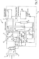
- FIG. 1 is a circuit schematic of a power converter according to the present invention.
- a power converter indicated generally by the reference numeral 1, comprising a converter input 3, a converter output (not shown), a power factor pre-regulation stage 5, an isolation stage 7 and a control unit 9.
- the power converter 1 further comprises an input filter 11 and an input bridge 13.
- the power factor pre-regulation stage 5 comprises a buck converter 15, which in turn comprises a buck controller 17, a buck switch 19, a buck inductor 21 and a buck diode 23.
- the buck converter 15 feeds a bulk capacitor 25.
- the isolation stage 7 comprises an isolation unit 27.
- the control unit 9 comprises a differential sensing circuit 29, a comparator 31 and a gain adjustment switch 33.
- the control unit 9 further comprises a loop control circuit having a pair of resistors 35, 37, a pair of constant voltage sources 39, 41, an error amplifier 43, a pair of capacitors 45, 47 and a further pair of resistors 49, 51.
- the control unit 9 further comprises a low pass filter 53 and a capacitor 55.
- the power converter input 3 is connected to the AC line input and the AC line input is passed through the input filter 11 and the input bridge 13.
- the buck controller 17 operates the buck switch 19 to control the flow of current to the bulk capacitor 25.
- the differential sensing unit 29 measures the voltage across the bulk capacitor 25 and this value is passed to the comparator 31.
- the comparator 31 compares the value of voltage across the bulk capacitor 25 with a threshold voltage which is marginally less than the low point associated with normal full load ripple voltage. If it is determined that the voltage across bulk capacitor 25 is less than the threshold voltage, the comparator 31 sends a signal to the gain adjustment switch 33, provided by way of a field effect transistor (FET) and turns the FET on.
- FET field effect transistor
- the comparator 31 is used to switch in the extra gain to the circuit.
- the error amplifier 43 is allowed to function at all times with the effective value of input resistance being changed by switching in a resistor in parallel to the resistor already in place using a MOSFET switch.
- the comparator 31 gates the MOSFET switch 33. It will be understood that when the switching is carried out current will be drawn from the line indirectly as the initial action of increasing the gain is carried out.
- transient conditions may be anticipated by monitoring the isolation stage output current and providing a feedforward signal to the adjusted line current.
- a current sense signal 57 is taken from the isolation stage 7 and delivered to the low pass filter 53.
- the fast override action is initiated and additional line current is sent through the buck pre-regulator stage to the bulk capacitor. In this way, the voltage across the bulk capacitor 25 may be kept sufficient to allow the power converter 1 to operate within pre-defined parameters.
- the additional line current has been provided by reducing the input resistance to the buck pre-regulation stage. It will be understood however that this may be achieved in a number of different ways, but the reduction of resistance is seen as a particularly useful and simple way of implementing the increase in line current to the bulk capacitor.
- the fast control method of monitoring the isolation stage output current may be implemented with or without the control loop monitoring the voltage across the bulk capacitor. By monitoring the bulk capacitor voltage, it is necessary for the bulk capacitor voltage to drop below the threshold level in order for the control mechanism to kick in.
- the invention could be carried out with other pre-regulation stage apparatus, however it is envisaged that the buck power factor correction circuit is preferred as this implementation is easily current limited and allows minimisation of the bulk capacitor size. This allows for reduction in the cost of the circuitry as well as greater efficiency in the output stages and improved duty cycle in the buck converter stage which leads to reduced stresses in the devices.
Landscapes
- Engineering & Computer Science (AREA)
- Physics & Mathematics (AREA)
- Electromagnetism (AREA)
- General Physics & Mathematics (AREA)
- Radar, Positioning & Navigation (AREA)
- Automation & Control Theory (AREA)
- Power Engineering (AREA)
- Rectifiers (AREA)
- Dc-Dc Converters (AREA)
Claims (12)
- Convertisseur de puissance (1) comprenant une entrée de convertisseur (3), une sortie de convertisseur, un étage de prérégulation du facteur de puissance (5), un étage d'isolation (7) et une unité de commande (9), l'étage de prérégulation du facteur de puissance comprenant en outre un circuit de correction du facteur de puissance (PFC) abaisseur (15) mis en oeuvre en utilisant une excitation côté bas et une détection de courant côté bas et un condensateur de masse (25), le circuit PFC abaisseur délivrant un courant au condensateur de masse en fonction de paramètres de régulation prédéterminés, l'unité de commande (9) comprenant un moyen pour mesurer des paramètres de fonctionnement du circuit du convertisseur de puissance, caractérisé par
un moyen pour amener le circuit PFC abaisseur (15) à délivrer un courant de ligne au condensateur de masse (25) qui est supplémentaire au courant de ligne de régulation en réponse aux paramètres de circuit mesurés du convertisseur de puissance quand l'unité de commande détecte que le convertisseur de puissance est sur le point de fonctionner à l'extérieur desdits paramètres de régulation, et un circuit de commande en boucle, et le moyen pour amener le circuit PFC abaisseur (15) à délivrer un courant de ligne supplémentaire au condensateur de masse (25) en réponse aux paramètres de circuit mesurés du convertisseur de puissance comprend l'augmentation du gain de boucle du circuit de commande en boucle. - Convertisseur de puissance (1) selon la revendication 1 dans lequel le moyen pour amener le circuit PFC abaisseur (15) à délivrer un courant de ligne supplémentaire au condensateur de masse (25) comprend un premier chemin de courant renfermant une première résistance (37), qui fournit un chemin pour le courant pendant le fonctionnement normal, et un deuxième chemin de courant ayant un commutateur (33) et une deuxième résistance (35) avec une valeur de résistance inférieure à celle de la première résistance (37), le commutateur (33) étant utilisable pour fournir le deuxième chemin alternatif au courant de telle sorte que le courant peut circuler à travers le deuxième chemin, réduisant ainsi la valeur de résistance du circuit PFC abaisseur.
- Convertisseur de puissance (1) selon la revendication 1 ou 2 dans lequel le circuit de commande en boucle comprend un amplificateur d'erreur (43).
- Convertisseur de puissance (1) selon une quelconque revendication précédente dans lequel le moyen des unités de commande (9) pour mesurer des paramètres de circuit du convertisseur de puissance comprend en outre un moyen (29) pour mesurer la tension aux bornes du condensateur de masse (25).
- Convertisseur de puissance (1) selon la revendication 4 dans lequel l'unité de commande (9) exagère la réponse à une baisse de la tension aux bornes du condensateur de masse (25) afin de restaurer la tension aux bornes du condensateur de masse dans un laps de temps aussi court que possible.
- Convertisseur de puissance (1) selon la revendication 4 ou 5 dans lequel l'unité de commande (9) comprend en outre un comparateur (31) pour comparer la valeur mesurée de la tension du condensateur de masse à une valeur seuil de tension de condensateur de masse, et lorsque la valeur mesurée chute au-dessous de la valeur seuil, un courant supplémentaire est délivré au condensateur de masse (25).
- Convertisseur de puissance (1) selon la revendication 6 dans lequel la valeur seuil de tension du condensateur de masse est une tension inférieure au point bas associé à une tension d'ondulation à pleine charge normale.
- Convertisseur de puissance (1) selon une quelconque revendication précédente dans lequel le moyen de l'unité de commande (9) pour mesurer des paramètres de circuit du convertisseur de puissance comprend en outre un moyen pour mesurer le courant à la sortie de l'étage d'isolation (27).
- Convertisseur de puissance (1) selon la revendication 8 dans lequel le moyen pour amener le circuit PFC abaisseur à délivrer un courant de ligne supplémentaire au condensateur de masse comprend la délivrance d'un signal de précompensation, en réponse à la valeur mesurée du courant à la sortie de l'étage d'isolation, pour ajuster la quantité de courant de ligne alimentant le condensateur de masse (25).
- Convertisseur de puissance (1) selon la revendication 8 ou 9 dans lequel l'unité de commande comprend en outre un réseau à retard.
- Convertisseur de puissance (1) selon la revendication 10 dans lequel le réseau à retard comprend en outre un filtre passe-bas (53).
- Convertisseur de puissance (1) selon une quelconque revendication précédente dans lequel l'unité de commande est pourvue d'un ajustement de synchronisation pour réduire la distorsion du courant de ligne.
Applications Claiming Priority (2)
| Application Number | Priority Date | Filing Date | Title |
|---|---|---|---|
| IE2006/0187A IE85947B1 (en) | 2006-03-10 | A power converter | |
| PCT/IE2007/000036 WO2007105189A1 (fr) | 2006-03-10 | 2007-03-12 | Convertisseur de puissance |
Publications (2)
| Publication Number | Publication Date |
|---|---|
| EP1994460A1 EP1994460A1 (fr) | 2008-11-26 |
| EP1994460B1 true EP1994460B1 (fr) | 2017-11-15 |
Family
ID=38066660
Family Applications (1)
| Application Number | Title | Priority Date | Filing Date |
|---|---|---|---|
| EP07713255.3A Not-in-force EP1994460B1 (fr) | 2006-03-10 | 2007-03-12 | Convertisseur de puissance |
Country Status (3)
| Country | Link |
|---|---|
| US (1) | US8198873B2 (fr) |
| EP (1) | EP1994460B1 (fr) |
| WO (1) | WO2007105189A1 (fr) |
Families Citing this family (10)
| Publication number | Priority date | Publication date | Assignee | Title |
|---|---|---|---|---|
| US8233298B2 (en) | 2008-06-05 | 2012-07-31 | Delta Electronics, Inc. | Power factor correction rectifier that operates efficiently over a range of input voltage conditions |
| RU2399084C1 (ru) * | 2009-09-23 | 2010-09-10 | Государственное образовательное учреждение высшего профессионального образования "Рыбинская государственная авиационная технологическая академия имени П.А. Соловьева" | Регулятор переменного напряжения |
| FR2973966B1 (fr) * | 2011-04-05 | 2014-01-17 | Atlantic Industrie Sas | Convertisseur ca/cc |
| TWI542127B (zh) | 2012-01-03 | 2016-07-11 | 財團法人工業技術研究院 | 降壓型主動式功因修正裝置 |
| KR101422962B1 (ko) | 2012-12-28 | 2014-07-28 | 서울시립대학교 산학협력단 | 역률 개선 회로 |
| TWI536206B (zh) * | 2013-11-05 | 2016-06-01 | 緯創資通股份有限公司 | 操作體的定位方法及裝置以及深度判定方法及裝置 |
| US11637493B2 (en) * | 2020-11-23 | 2023-04-25 | Robert S. Wrathall | Electrical circuits for power factor correction by measurement and removal of overtones and power factor maximization |
| US12294295B2 (en) * | 2020-11-23 | 2025-05-06 | Robert S. Wrathall | Systems and methods of unwanted harmonic content removal for power conversion |
| US10998815B1 (en) * | 2020-11-23 | 2021-05-04 | Robert S. Wrathall | Electrical circuits for power factor correction by measurement and removal of overtones |
| US20220244320A1 (en) * | 2021-01-29 | 2022-08-04 | Texas Instruments Incorporated | Low cost method-b high voltage isolation screen test |
Family Cites Families (11)
| Publication number | Priority date | Publication date | Assignee | Title |
|---|---|---|---|---|
| US4533986A (en) * | 1983-10-31 | 1985-08-06 | General Electric Company | Compact electrical power supply for signal processing applications |
| JPH0296413A (ja) * | 1988-09-30 | 1990-04-09 | Matsushita Electric Ind Co Ltd | 可変利得増幅装置 |
| US5134355A (en) * | 1990-12-31 | 1992-07-28 | Texas Instruments Incorporated | Power factor correction control for switch-mode power converters |
| US5144222A (en) * | 1991-01-07 | 1992-09-01 | Edward Herbert | Apparatus for controlling the input impedance of a power converter |
| US5900701A (en) * | 1996-05-21 | 1999-05-04 | Allied Energy Services International, Inc. | High frequency electronic ballast for lighting |
| US6531854B2 (en) * | 2001-03-30 | 2003-03-11 | Champion Microelectronic Corp. | Power factor correction circuit arrangement |
| DK3589081T3 (da) * | 2004-03-15 | 2024-03-18 | Signify North America Corp | Effektstyringfremgangsmåder og -apparat |
| EP1949527A2 (fr) * | 2005-10-10 | 2008-07-30 | Commergy Technologies Limited | Convertisseur de puissance |
| US7848117B2 (en) * | 2007-01-22 | 2010-12-07 | Power Integrations, Inc. | Control arrangement for a resonant mode power converter |
| US7911812B2 (en) * | 2007-01-22 | 2011-03-22 | Power Integrations, Inc. | Control arrangement for a PFC power converter |
| US7554473B2 (en) * | 2007-05-02 | 2009-06-30 | Cirrus Logic, Inc. | Control system using a nonlinear delta-sigma modulator with nonlinear process modeling |
-
2007
- 2007-03-12 EP EP07713255.3A patent/EP1994460B1/fr not_active Not-in-force
- 2007-03-12 US US12/282,330 patent/US8198873B2/en active Active
- 2007-03-12 WO PCT/IE2007/000036 patent/WO2007105189A1/fr not_active Ceased
Non-Patent Citations (1)
| Title |
|---|
| None * |
Also Published As
| Publication number | Publication date |
|---|---|
| US20100013444A1 (en) | 2010-01-21 |
| IE20060187A1 (en) | 2007-11-14 |
| WO2007105189A1 (fr) | 2007-09-20 |
| US8198873B2 (en) | 2012-06-12 |
| EP1994460A1 (fr) | 2008-11-26 |
Similar Documents
| Publication | Publication Date | Title |
|---|---|---|
| EP1994460B1 (fr) | Convertisseur de puissance | |
| EP2043242B1 (fr) | Convertisseur de puissance avec haute dynamique et PFC | |
| US8018694B1 (en) | Over-current protection for a power converter | |
| EP0884746B1 (fr) | Régulateur à commutation synchrone avec chute de tension d'interrupteur pour détection de courant | |
| US8299773B2 (en) | System and method for limiting input-current surge in a switching mode power supply | |
| US6965502B2 (en) | System, device and method for providing voltage regulation to a microelectronic device | |
| TWI531883B (zh) | 用於低待機電流切換調節器的方法及設備 | |
| US7492132B2 (en) | Switching regulator | |
| US9621036B2 (en) | Circuits and techniques for improving regulation in a regulator having more than one mode of operation | |
| US9270162B2 (en) | Switching regulator and electronic device | |
| TWI539256B (zh) | 用於切換模式調節器之動態下降之系統與方法 | |
| US10790737B2 (en) | Current threshold regulation method used in switching converters | |
| US9083237B2 (en) | Circuits and methods for controlling a DC/DC converter | |
| US8400133B2 (en) | Output current detection of a voltage regulator | |
| US10326362B2 (en) | Switching regulator | |
| US9000705B2 (en) | Power controller | |
| US10756621B2 (en) | Voltage regulators with controlled output voltage and the method thereof | |
| WO2002031951A2 (fr) | Systeme et procede de regulation de puissance hautement mis en phase au moyen d'un controle de compensation adaptif | |
| JP4591571B2 (ja) | 電源装置 | |
| US20170331363A1 (en) | Current Limited Power Converter Circuits And Methods | |
| WO2020076499A1 (fr) | Circuits intégrés dotés de blocages de limites de courant et de blocages de sauts | |
| US12244221B2 (en) | Method and circuit arrangement for controlling a switched-mode power supply | |
| JP2010136506A (ja) | Dc/dcコンバータ | |
| US20080205087A1 (en) | Power supply feedback control using sensed duty cycle | |
| CN114944753A (zh) | 用于缓解dc-dc调节器负载转储瞬态的电感电流分流线性控制技术 |
Legal Events
| Date | Code | Title | Description |
|---|---|---|---|
| PUAI | Public reference made under article 153(3) epc to a published international application that has entered the european phase |
Free format text: ORIGINAL CODE: 0009012 |
|
| 17P | Request for examination filed |
Effective date: 20081010 |
|
| AK | Designated contracting states |
Kind code of ref document: A1 Designated state(s): DE FR GB NL |
|
| DAX | Request for extension of the european patent (deleted) | ||
| RBV | Designated contracting states (corrected) |
Designated state(s): DE FR GB NL |
|
| 17Q | First examination report despatched |
Effective date: 20111222 |
|
| GRAP | Despatch of communication of intention to grant a patent |
Free format text: ORIGINAL CODE: EPIDOSNIGR1 |
|
| INTG | Intention to grant announced |
Effective date: 20170515 |
|
| GRAS | Grant fee paid |
Free format text: ORIGINAL CODE: EPIDOSNIGR3 |
|
| GRAJ | Information related to disapproval of communication of intention to grant by the applicant or resumption of examination proceedings by the epo deleted |
Free format text: ORIGINAL CODE: EPIDOSDIGR1 |
|
| GRAL | Information related to payment of fee for publishing/printing deleted |
Free format text: ORIGINAL CODE: EPIDOSDIGR3 |
|
| GRAR | Information related to intention to grant a patent recorded |
Free format text: ORIGINAL CODE: EPIDOSNIGR71 |
|
| GRAA | (expected) grant |
Free format text: ORIGINAL CODE: 0009210 |
|
| INTC | Intention to grant announced (deleted) | ||
| INTG | Intention to grant announced |
Effective date: 20171005 |
|
| AK | Designated contracting states |
Kind code of ref document: B1 Designated state(s): DE FR GB NL |
|
| REG | Reference to a national code |
Ref country code: GB Ref legal event code: FG4D |
|
| REG | Reference to a national code |
Ref country code: DE Ref legal event code: R096 Ref document number: 602007053029 Country of ref document: DE |
|
| REG | Reference to a national code |
Ref country code: FR Ref legal event code: PLFP Year of fee payment: 12 |
|
| REG | Reference to a national code |
Ref country code: NL Ref legal event code: MP Effective date: 20171115 |
|
| PG25 | Lapsed in a contracting state [announced via postgrant information from national office to epo] |
Ref country code: NL Free format text: LAPSE BECAUSE OF FAILURE TO SUBMIT A TRANSLATION OF THE DESCRIPTION OR TO PAY THE FEE WITHIN THE PRESCRIBED TIME-LIMIT Effective date: 20171115 |
|
| REG | Reference to a national code |
Ref country code: DE Ref legal event code: R097 Ref document number: 602007053029 Country of ref document: DE |
|
| PLBE | No opposition filed within time limit |
Free format text: ORIGINAL CODE: 0009261 |
|
| STAA | Information on the status of an ep patent application or granted ep patent |
Free format text: STATUS: NO OPPOSITION FILED WITHIN TIME LIMIT |
|
| 26N | No opposition filed |
Effective date: 20180817 |
|
| PGFP | Annual fee paid to national office [announced via postgrant information from national office to epo] |
Ref country code: GB Payment date: 20220225 Year of fee payment: 16 Ref country code: DE Payment date: 20220217 Year of fee payment: 16 |
|
| PGFP | Annual fee paid to national office [announced via postgrant information from national office to epo] |
Ref country code: FR Payment date: 20220221 Year of fee payment: 16 |
|
| REG | Reference to a national code |
Ref country code: DE Ref legal event code: R119 Ref document number: 602007053029 Country of ref document: DE |
|
| GBPC | Gb: european patent ceased through non-payment of renewal fee |
Effective date: 20230312 |
|
| PG25 | Lapsed in a contracting state [announced via postgrant information from national office to epo] |
Ref country code: GB Free format text: LAPSE BECAUSE OF NON-PAYMENT OF DUE FEES Effective date: 20230312 |
|
| PG25 | Lapsed in a contracting state [announced via postgrant information from national office to epo] |
Ref country code: GB Free format text: LAPSE BECAUSE OF NON-PAYMENT OF DUE FEES Effective date: 20230312 Ref country code: FR Free format text: LAPSE BECAUSE OF NON-PAYMENT OF DUE FEES Effective date: 20230331 Ref country code: DE Free format text: LAPSE BECAUSE OF NON-PAYMENT OF DUE FEES Effective date: 20231003 |