EP1998311A2 - Anzeigevorrichtung mit Flachbildschirm - Google Patents
Anzeigevorrichtung mit Flachbildschirm Download PDFInfo
- Publication number
- EP1998311A2 EP1998311A2 EP08157366A EP08157366A EP1998311A2 EP 1998311 A2 EP1998311 A2 EP 1998311A2 EP 08157366 A EP08157366 A EP 08157366A EP 08157366 A EP08157366 A EP 08157366A EP 1998311 A2 EP1998311 A2 EP 1998311A2
- Authority
- EP
- European Patent Office
- Prior art keywords
- data
- signal
- value
- flat panel
- panel display
- Prior art date
- Legal status (The legal status is an assumption and is not a legal conclusion. Google has not performed a legal analysis and makes no representation as to the accuracy of the status listed.)
- Withdrawn
Links
Images


Classifications
-
- G—PHYSICS
- G09—EDUCATION; CRYPTOGRAPHY; DISPLAY; ADVERTISING; SEALS
- G09G—ARRANGEMENTS OR CIRCUITS FOR CONTROL OF INDICATING DEVICES USING STATIC MEANS TO PRESENT VARIABLE INFORMATION
- G09G3/00—Control arrangements or circuits, of interest only in connection with visual indicators other than cathode-ray tubes
- G09G3/20—Control arrangements or circuits, of interest only in connection with visual indicators other than cathode-ray tubes for presentation of an assembly of a number of characters, e.g. a page, by composing the assembly by combination of individual elements arranged in a matrix no fixed position being assigned to or needed to be assigned to the individual characters or partial characters
- G09G3/22—Control arrangements or circuits, of interest only in connection with visual indicators other than cathode-ray tubes for presentation of an assembly of a number of characters, e.g. a page, by composing the assembly by combination of individual elements arranged in a matrix no fixed position being assigned to or needed to be assigned to the individual characters or partial characters using controlled light sources
- G09G3/28—Control arrangements or circuits, of interest only in connection with visual indicators other than cathode-ray tubes for presentation of an assembly of a number of characters, e.g. a page, by composing the assembly by combination of individual elements arranged in a matrix no fixed position being assigned to or needed to be assigned to the individual characters or partial characters using controlled light sources using luminous gas-discharge panels, e.g. plasma panels
- G09G3/288—Control arrangements or circuits, of interest only in connection with visual indicators other than cathode-ray tubes for presentation of an assembly of a number of characters, e.g. a page, by composing the assembly by combination of individual elements arranged in a matrix no fixed position being assigned to or needed to be assigned to the individual characters or partial characters using controlled light sources using luminous gas-discharge panels, e.g. plasma panels using AC panels
- G09G3/296—Driving circuits for producing the waveforms applied to the driving electrodes
-
- G—PHYSICS
- G09—EDUCATION; CRYPTOGRAPHY; DISPLAY; ADVERTISING; SEALS
- G09G—ARRANGEMENTS OR CIRCUITS FOR CONTROL OF INDICATING DEVICES USING STATIC MEANS TO PRESENT VARIABLE INFORMATION
- G09G3/00—Control arrangements or circuits, of interest only in connection with visual indicators other than cathode-ray tubes
- G09G3/20—Control arrangements or circuits, of interest only in connection with visual indicators other than cathode-ray tubes for presentation of an assembly of a number of characters, e.g. a page, by composing the assembly by combination of individual elements arranged in a matrix no fixed position being assigned to or needed to be assigned to the individual characters or partial characters
- G09G3/22—Control arrangements or circuits, of interest only in connection with visual indicators other than cathode-ray tubes for presentation of an assembly of a number of characters, e.g. a page, by composing the assembly by combination of individual elements arranged in a matrix no fixed position being assigned to or needed to be assigned to the individual characters or partial characters using controlled light sources
- G09G3/28—Control arrangements or circuits, of interest only in connection with visual indicators other than cathode-ray tubes for presentation of an assembly of a number of characters, e.g. a page, by composing the assembly by combination of individual elements arranged in a matrix no fixed position being assigned to or needed to be assigned to the individual characters or partial characters using controlled light sources using luminous gas-discharge panels, e.g. plasma panels
- G09G3/288—Control arrangements or circuits, of interest only in connection with visual indicators other than cathode-ray tubes for presentation of an assembly of a number of characters, e.g. a page, by composing the assembly by combination of individual elements arranged in a matrix no fixed position being assigned to or needed to be assigned to the individual characters or partial characters using controlled light sources using luminous gas-discharge panels, e.g. plasma panels using AC panels
- G09G3/291—Control arrangements or circuits, of interest only in connection with visual indicators other than cathode-ray tubes for presentation of an assembly of a number of characters, e.g. a page, by composing the assembly by combination of individual elements arranged in a matrix no fixed position being assigned to or needed to be assigned to the individual characters or partial characters using controlled light sources using luminous gas-discharge panels, e.g. plasma panels using AC panels controlling the gas discharge to control a cell condition, e.g. by means of specific pulse shapes
- G09G3/292—Control arrangements or circuits, of interest only in connection with visual indicators other than cathode-ray tubes for presentation of an assembly of a number of characters, e.g. a page, by composing the assembly by combination of individual elements arranged in a matrix no fixed position being assigned to or needed to be assigned to the individual characters or partial characters using controlled light sources using luminous gas-discharge panels, e.g. plasma panels using AC panels controlling the gas discharge to control a cell condition, e.g. by means of specific pulse shapes for reset discharge, priming discharge or erase discharge occurring in a phase other than addressing
- G09G3/2927—Details of initialising
-
- G—PHYSICS
- G09—EDUCATION; CRYPTOGRAPHY; DISPLAY; ADVERTISING; SEALS
- G09G—ARRANGEMENTS OR CIRCUITS FOR CONTROL OF INDICATING DEVICES USING STATIC MEANS TO PRESENT VARIABLE INFORMATION
- G09G3/00—Control arrangements or circuits, of interest only in connection with visual indicators other than cathode-ray tubes
- G09G3/20—Control arrangements or circuits, of interest only in connection with visual indicators other than cathode-ray tubes for presentation of an assembly of a number of characters, e.g. a page, by composing the assembly by combination of individual elements arranged in a matrix no fixed position being assigned to or needed to be assigned to the individual characters or partial characters
- G09G3/22—Control arrangements or circuits, of interest only in connection with visual indicators other than cathode-ray tubes for presentation of an assembly of a number of characters, e.g. a page, by composing the assembly by combination of individual elements arranged in a matrix no fixed position being assigned to or needed to be assigned to the individual characters or partial characters using controlled light sources
- G09G3/28—Control arrangements or circuits, of interest only in connection with visual indicators other than cathode-ray tubes for presentation of an assembly of a number of characters, e.g. a page, by composing the assembly by combination of individual elements arranged in a matrix no fixed position being assigned to or needed to be assigned to the individual characters or partial characters using controlled light sources using luminous gas-discharge panels, e.g. plasma panels
- G09G3/288—Control arrangements or circuits, of interest only in connection with visual indicators other than cathode-ray tubes for presentation of an assembly of a number of characters, e.g. a page, by composing the assembly by combination of individual elements arranged in a matrix no fixed position being assigned to or needed to be assigned to the individual characters or partial characters using controlled light sources using luminous gas-discharge panels, e.g. plasma panels using AC panels
- G09G3/291—Control arrangements or circuits, of interest only in connection with visual indicators other than cathode-ray tubes for presentation of an assembly of a number of characters, e.g. a page, by composing the assembly by combination of individual elements arranged in a matrix no fixed position being assigned to or needed to be assigned to the individual characters or partial characters using controlled light sources using luminous gas-discharge panels, e.g. plasma panels using AC panels controlling the gas discharge to control a cell condition, e.g. by means of specific pulse shapes
- G09G3/293—Control arrangements or circuits, of interest only in connection with visual indicators other than cathode-ray tubes for presentation of an assembly of a number of characters, e.g. a page, by composing the assembly by combination of individual elements arranged in a matrix no fixed position being assigned to or needed to be assigned to the individual characters or partial characters using controlled light sources using luminous gas-discharge panels, e.g. plasma panels using AC panels controlling the gas discharge to control a cell condition, e.g. by means of specific pulse shapes for address discharge
-
- G—PHYSICS
- G09—EDUCATION; CRYPTOGRAPHY; DISPLAY; ADVERTISING; SEALS
- G09G—ARRANGEMENTS OR CIRCUITS FOR CONTROL OF INDICATING DEVICES USING STATIC MEANS TO PRESENT VARIABLE INFORMATION
- G09G2310/00—Command of the display device
- G09G2310/02—Addressing, scanning or driving the display screen or processing steps related thereto
- G09G2310/0202—Addressing of scan or signal lines
- G09G2310/0218—Addressing of scan or signal lines with collection of electrodes in groups for n-dimensional addressing
-
- G—PHYSICS
- G09—EDUCATION; CRYPTOGRAPHY; DISPLAY; ADVERTISING; SEALS
- G09G—ARRANGEMENTS OR CIRCUITS FOR CONTROL OF INDICATING DEVICES USING STATIC MEANS TO PRESENT VARIABLE INFORMATION
- G09G2310/00—Command of the display device
- G09G2310/02—Addressing, scanning or driving the display screen or processing steps related thereto
- G09G2310/0264—Details of driving circuits
- G09G2310/0275—Details of drivers for data electrodes, other than drivers for liquid crystal, plasma or OLED displays, not related to handling digital grey scale data or to communication of data to the pixels by means of a current
-
- G—PHYSICS
- G09—EDUCATION; CRYPTOGRAPHY; DISPLAY; ADVERTISING; SEALS
- G09G—ARRANGEMENTS OR CIRCUITS FOR CONTROL OF INDICATING DEVICES USING STATIC MEANS TO PRESENT VARIABLE INFORMATION
- G09G2310/00—Command of the display device
- G09G2310/02—Addressing, scanning or driving the display screen or processing steps related thereto
- G09G2310/0264—Details of driving circuits
- G09G2310/0297—Special arrangements with multiplexing or demultiplexing of display data in the drivers for data electrodes, in a pre-processing circuitry delivering display data to said drivers or in the matrix panel, e.g. multiplexing plural data signals to one D/A converter or demultiplexing the D/A converter output to multiple columns
-
- G—PHYSICS
- G09—EDUCATION; CRYPTOGRAPHY; DISPLAY; ADVERTISING; SEALS
- G09G—ARRANGEMENTS OR CIRCUITS FOR CONTROL OF INDICATING DEVICES USING STATIC MEANS TO PRESENT VARIABLE INFORMATION
- G09G2310/00—Command of the display device
- G09G2310/04—Partial updating of the display screen
-
- G—PHYSICS
- G09—EDUCATION; CRYPTOGRAPHY; DISPLAY; ADVERTISING; SEALS
- G09G—ARRANGEMENTS OR CIRCUITS FOR CONTROL OF INDICATING DEVICES USING STATIC MEANS TO PRESENT VARIABLE INFORMATION
- G09G2310/00—Command of the display device
- G09G2310/06—Details of flat display driving waveforms
- G09G2310/066—Waveforms comprising a gently increasing or decreasing portion, e.g. ramp
-
- G—PHYSICS
- G09—EDUCATION; CRYPTOGRAPHY; DISPLAY; ADVERTISING; SEALS
- G09G—ARRANGEMENTS OR CIRCUITS FOR CONTROL OF INDICATING DEVICES USING STATIC MEANS TO PRESENT VARIABLE INFORMATION
- G09G2310/00—Command of the display device
- G09G2310/08—Details of timing specific for flat panels, other than clock recovery
-
- G—PHYSICS
- G09—EDUCATION; CRYPTOGRAPHY; DISPLAY; ADVERTISING; SEALS
- G09G—ARRANGEMENTS OR CIRCUITS FOR CONTROL OF INDICATING DEVICES USING STATIC MEANS TO PRESENT VARIABLE INFORMATION
- G09G2330/00—Aspects of power supply; Aspects of display protection and defect management
- G09G2330/02—Details of power systems and of start or stop of display operation
- G09G2330/021—Power management, e.g. power saving
-
- G—PHYSICS
- G09—EDUCATION; CRYPTOGRAPHY; DISPLAY; ADVERTISING; SEALS
- G09G—ARRANGEMENTS OR CIRCUITS FOR CONTROL OF INDICATING DEVICES USING STATIC MEANS TO PRESENT VARIABLE INFORMATION
- G09G2330/00—Aspects of power supply; Aspects of display protection and defect management
- G09G2330/04—Display protection
- G09G2330/045—Protection against panel overheating
-
- G—PHYSICS
- G09—EDUCATION; CRYPTOGRAPHY; DISPLAY; ADVERTISING; SEALS
- G09G—ARRANGEMENTS OR CIRCUITS FOR CONTROL OF INDICATING DEVICES USING STATIC MEANS TO PRESENT VARIABLE INFORMATION
- G09G2330/00—Aspects of power supply; Aspects of display protection and defect management
- G09G2330/06—Handling electromagnetic interferences [EMI], covering emitted as well as received electromagnetic radiation
-
- G—PHYSICS
- G09—EDUCATION; CRYPTOGRAPHY; DISPLAY; ADVERTISING; SEALS
- G09G—ARRANGEMENTS OR CIRCUITS FOR CONTROL OF INDICATING DEVICES USING STATIC MEANS TO PRESENT VARIABLE INFORMATION
- G09G2370/00—Aspects of data communication
- G09G2370/08—Details of image data interface between the display device controller and the data line driver circuit
Definitions
- the present invention is directed to a flat display device and more specifically to a device supplying a data signal to a flat display panel.
- PDP devices Out of the flat panel display devices, PDP devices have some advantages such as slim and large size, simplified structure, easy-to-manufacture characteristics, as well as raised brightness and emission efficiency.
- a conventional PDP device has a data integrated circuit ("IC") that applies a driving signal to a plasma display panel.
- IC data integrated circuit
- the data IC generates a driving signal by switching operations of plural switches included in the data IC based on driving data.
- An aspect of the present invention provides a flat panel display device that is capable of reducing EMI occuring in a driving circuit and ensuring a sufficient timing margin that can be reduced according to high rate switching operations of the driving circuit in supplying a data signal to a flat panel display panel such as a plasma display panel.
- a flat panel display device includes a controller processing an inputted image signal to generate a data signal to be supplied to the panel, generating a first signal having information on whether two or more consecutive data of the data signal comply with each other and outputting the first signal along with the data signal; and a data driver generating a clock signal using the data signal and the first signal inputted from the controller and supplying the data signal to the panel using the generated clock signal.
- an exemplary PDP device is exemplified as a flat panel display device according to an exemplary embodiment of the present invention
- the present invention is not limited to such a PDP device, and for example, the present invention may apply to the other flat panel display devices, such as LCD devices, OLED (Organic Light Emitting Diode) devices, etc.
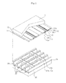
- FIG. 1 is a perspective view illustrating a construction of a plasma display panel according to an exemplary embodiment of the present invention.
- a PDP includes a pair of sustaining electrode formed on an upper substrate 10 and an address electrode formed on a lower substrate 20.
- the pair of sustaining electrode includes a scan electrode 11 and a sustain electrode 12.
- the scan electrode 11 includes a transparent electrode 11 a generally made of indium tin oxide (ITO) and a bus electrode 11 b.
- the sustain electrode 12 includes a transparent electrode 12a generally made of indium tin oxide (ITO) and a bus electrode 12b.
- the bus electrodes 11 b and 12b may be formed in a single layer of a metal such as Ag and Cr, or in a multiple layer of Cr/Cu/Cr or Cr/Al/Cr.
- the bus electrodes 11 b and 12b are stacked on the transparent electrodes 11 a and 12a, respectively, and serve to reduce voltage drop due to high-resistance transparent electrodes 11a and 12a.
- the pair of sustaining electrodes 11 and 12 may be formed of the bus electrodes 11 b and 12b without the transparent electrodes 11a and 12a, as well as in the stacked structure of the transparent electrodes 11 a and 12a and the bus electrodes 11 b and 12b.
- This structure help reduce the manufacturing costs of the PDP.
- the bus electrodes 11 b and 12b may be made of various materials as well as the above-listed materials.
- a black matrix (BM) 15 is positioned between the transparent electrode 11 a and the bus electrode 11 b and between the transparent electrode 12a and the bus electrode 12b.
- the black matrix 15 serves to absorb external light to reduce the reflection of light and improve purity and contrast ratio of the upper substrate 10.
- the black matrix 15 is formed on the upper substrate.
- the black matrix 15 may include a first black matrix 15 and second black matrix 11c and 12c.
- the first black matrix 15 is formed to overlap a barrier rib 21.
- the second black matrix 11 c is formed between the transparent electrode 11a and the bus electrode 11 b, and the second black matrix 12c is formed between the transparent electrode 12a and the bus electrode 12b.
- the first black matrix 15 and the second black matrixes 11c and 12c which are called “black layer” or “black electrode layer”, are simultaneously formed and physically connected to each other, or non-simultaneously formed and physically separated from each other.
- first black matrix and the second black matrixes are physically connected to each other, they may be made of the same material, but otherwise, they may be made of different materials.
- An upper dielectric layer 13 and a protection layer 14 are stacked on the upper substrate 10 on which the scan electrode 11 and the sustain electrode 12 have been arranged in parallel to each other.
- the upper dielectric layer 13 on which electric charges generated by discharge are accumulated may function to protect the pair of sustaining electrodes 11 and 12.
- the protection layer 14 protects the upper dielectric layer 13 from sputtering caused by the electric charges generated during gas discharge and raise discharge efficiency of secondary electrons.
- An address electrode 22 is formed in a direction of intersecting the scan electrode 11 and the sustain electrode 12.
- a lower dielectric layer 23 and the barrier rib 21 are formed on the lower substrate 20 on which the address electrode 22 has been arranged.
- a phosphor layer 23 is formed on the surface of the lower dielectric layer 24 and the barrier rib 21.
- the barrier rib 21 includes a vertical barrier rib 21 a and a horizontal barrier rib 21 b crossing the vertical barrier rib 21a.
- the barrier rib 21 physically separates a discharge cell from other discharge cells, and prevents the leakage to neighboring discharge cells of ultraviolet rays and visible light generated by discharge.
- barrier ribs may be available besides the barrier rib 21 shown in FIG. 1 according to an exemplary embodiment of the present invention.
- the barrier rib 21 may have various structures other than the structure illustrated in FIG. 1 .
- the barrier rib 21 may be configured so that the vertical barrier rib 21 a is different in height from the horizontal barrier rib 21 b-this is called "height-different type barrier rib”.
- the barrier rib 21 may be also configured so that at least one of the vertical barrier rib 21a and the horizontal barrier rib 21 b has a channel that can be used as an exhaust gas pathway- this is called "channel type barrier rib”.
- the barrier rib 21 may be configured so that at least one of the vertical barrier rib 21 a and the horizontal barrier rib 21 b has a hollow-this is called “hollow type barrier rib”.
- the horizontal barrier rib 21 b may be higher in height than the vertical barrier rib 21a.
- a channel or hollow may be formed in the horizontal barrier rib 21 b.
- red, green, and blue discharge cells are arranged on the same line in this exemplary embodiment of the present invention, they may be arranged in various manners.
- red, green, and blue discharge cells may be arranged in a shape of the Greek letter " ⁇ ".
- the discharge cell may be shaped as a pentagon, a hexagon, as well as a tetragon.
- the phosphor layer 23 may be excited by ultraviolet rays generated upon a gas discharge to emit visible light including red light, green light, and blue light.
- a mixed inert gas of He+Xe, Ne+Xe, or He+Ne+Xe is injected into a discharge space prepared between the upper/lower substrates 10 and 20 and the barrier rib 21.
- FIG. 2 is a view illustrating an array of electrodes included in a plasma display panel according to an exemplary embodiment of the present invention.
- plural discharge cells constituting a PDP may be arranged in a matrix pattern.
- Each of the discharge cells is arranged near an intersection of a scan electrode line Y1 to Ym, a sustain electrode line Z1 to Zm, and an address electrode line X1 to Xn.
- the scan electrode lines Y1 to Ym may be sequentially or simultaneously driven, and the sustain electrode lines Z1 to Zm may be simultaneously driven.
- the address electrode lines X1 to Xn may be driven simultaneously or in the order of an odd-numbered line and an even-numbered line.
- the electrode arrangement shown in FIG. 2 is only an example of the electrode arrangement in the PDP according to an exemplary embodiment of the present invention. Therefore, the present invention is not limited to the electrode arrangement and driving method shown in FIG. 2 .
- the present invention may employ a dual scan method, where two of the scan electrode lines Y1 to Ym are simultaneously scanned.
- the address electrode lines X1 to Xn may be divided in left and right parts or in upper and lower parts with respect to a central axis of the panel to be driven according to each of the divided parts.
- FIG. 3 is a timing diagram illustrating a time-division driving method of a plasma display panel according to an exemplary embodiment of the present invention, wherein one frame is divided into plural sub fields.
- a unit frame may be separated into, e.g. eight sub fields SF1 to SF8 for time-division gray scale display.
- Each of the sub field SF1 to SF8 includes a reset period (not shown), an address period A1 to A8, and a sustain period S1 to S8.
- a reset period may be omitted from at least one of the plural subfields.
- the reset period may exist only within the first sub field, or only within the first sub field and a sub field positioned between the first sub field and the last sub field.
- a display data signal is applied to the address electrode X and a corresponding scan pulse is sequentially applied to each scan electrode Y.
- a sustain pulse is alternately applied to the scan electrode Y and the sustain electrode Z, so that sustain discharge occurs in the discharge cells in which wall charges are generated during the address period A1 to A8.
- the brightness of the PDP is in proportion to the number of sustain discharge pulses generated during the sustain period S1 to S8 occupying a unit frame.
- the number of sustain pulses may be differently assigned to each sub field in the ratio of 1, 2, 4, 8, 16, 32, 64, and 128.
- the number of sustain discharges assigned to each subfield may be determined according to weight value of sub fields according to automatic power control (APC) stage.
- APC automatic power control
- FIG. 3 where one frame is divided into eight subfields, the present invention is not limited thereto, and the number of subfields constituting one frame may be varied depending on design and specifications. For example, one frame may be separated into more than eight subfields, such as 12 subfields and 16 subfields in order to drive the PDP.
- the number of sustain discharges assigned to each subfield may be varied considering gamma properties or panel characteristics.
- the degree of gray scale assigned to subfield SF4 may be lowered from 8 to 6
- the degree of gray scale assigned to subfield 6 may be raised from 32 to 34.
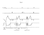
- FIG. 4 is a timing diagram illustrating a waveform of a driving signal of driving a plasma display panel according to an exemplary embodiment of the present invention.
- each subfield may include a pre-reset period, a reset-period, an address period, and a sustain period.
- the pre-reset period generates positive wall charges on the scan electrodes Y and negative wall charges on the sustain electrodes Z.
- the reset period initializes the overall discharge cells using the distribution of the wall charges formed during the pre-reset period.
- the address period selects discharge cells.
- the sustain period sustains discharge occurring in the selected discharge cells.
- a reset period includes a set-up period and a set-down period.
- a ramp-up waveform is simultaneously applied to the overall scan electrodes to cause tiny discharge in the whole discharge cells, and as a consequence, wall charges are generated.
- a ramp-down waveform which falls from a positive voltage whose peak is lower than that of the ramp-up waveform, is simultaneously applied to the whole scan electrodes Y to cause an erase discharge in the overall discharge cells, and accordingly, unnecessary charges are erased from space charges and wall charges generated by set-up discharge.
- a scan signal having a negative scan voltage Vsc is sequentially to the scan electrodes, and at the same time, a negative data signal is applied to the address electrode X.
- Address discharge occurs by the voltage difference between the scan signal and the data signal and wall charges generated during the reset period, and therefore, a cell is selected.
- a sustain bias voltage Vzb may be applied to the sustain electrodes during the address period to raise the efficiency of address discharge.
- the plural scan electrodes Y may be grouped into two or more, and scan signals may be sequentially applied to the scan electrode groups. And, each scan electrode group may be divided again into two or more sub groups, and scan signals may be sequentially supplied to the sub groups. For example, the plural scan electrodes Y may be divided into a first group and a second group, and scan signals are sequentially supplied to scan electrodes included into the first group and then to scan electrodes included into the second group.
- the plural scan electrodes Y may be divided into a first group including even-numbered scan electrodes and a second group including odd-numbered scan electrodes.
- the plural scan electrodes Y may be divided into a first group including scan electrodes located in an upper part of the panel and a second group including scan electrodes located in a lower part of the panel with respect of a central axis.
- the scan electrodes included in the first group may be divided again into a first sub group including even-numbered scan electrodes and a second sub group including odd-numbered scan electrodes, or a first sub group including scan electrodes located in an upper part and a second sub group including scan electrodes located in a lower part with respect to a central line of the first group.
- a sustain pulse having a sustain voltage Vs is alternately applied to the scan electrode and the sustain electrode to cause a sustain discharge in a type of surface discharge between the scan electrode and the sustain electrode.
- the first sustain signal and the last sustain signal may be larger in pulse width than the other sustain signals.
- the sub field may further include an erase period to erase wall charges remaining on the scan electrode and the sustain electrode of On-state cells selected during the address period by causing a weak discharge between the scan electrode and the sustain electrode.
- the erase period may be included in the overall subfields or some subfields, and an erase signal for causing a weak discharge may be applied to an electrode to which the last sustain pulse is not applied during the sustain period.
- the erase signal may include a gradually rising ramp signal, a low voltage wide pulse, a high voltage narrow pulse, an exponential signal, or a half-sinusoidal pulse.
- Plural pulses may be sequentially applied to the scan electrode and the sustain electrode to cause a weak discharge.
- the driving waveforms shown in FIG. 4 are only an example of signals to drive the plasma display panel according to an exemplary embodiment of the present invention, and the present invention is not limited to the driving waveforms shown in FIG. 4 .
- the pre reset period may be omitted from the sub field, and the polarity and voltage level of the driving waveforms shown in FIG. 4 may be modified as necessary.
- the erase signal may be also applied to the sustain electrode in order to erase wall charges after the sustain discharge has been complete.
- the sustain signal may be applied to either of the scan electrode Y or the sustain electrode Z to cause a sustain discharge, which is called "single sustain driving".
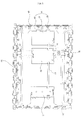
- FIG. 5 is a view illustrating a construction of a driving device of driving a plasma display panel according to an exemplary embodiment of the present invention.
- a heat-sink frame 30 is mounted on the rear surface of the panel to support the panel, and absorb and dissipate heat emanating from the panel.
- a printed circuit board (PCB) is mounted on the real side of the heat-sink 30 frame 30 to apply driving signals to the panel.
- On the printed circuit board may be arranged a data driver 50 for supplying a driving signal to the address electrodes of the panel, a scan driver 60 for supplying a driving signal to the scan electrodes of the panel, a sustain driver 70 for supplying a driving signal to the sustain electrodes of the panel, a controller for controlling the driving circuits, and a power supply unit (PSU) 90 for supplying electricity to each driving circuit.
- a data driver 50 for supplying a driving signal to the address electrodes of the panel
- a scan driver 60 for supplying a driving signal to the scan electrodes of the panel
- a sustain driver 70 for supplying a driving signal to the sustain electrodes of the panel
- a controller for controlling the driving circuits
- PSU power supply unit
- the data driver 50 supplies a driving signal to the address electrodes arranged on the panel so that only the discharge cells that cause a discharge may be selected out of the plural discharge cells formed on the panel.
- the data driver 50 may be mounted on either or both of the upper side or/and the lower side of the panel according to a single scan method or dual scan method.
- the data driver 50 includes a data IC (Integrated Circuit) to control a current applied to the address electrode.
- the data IC may cause considerable heat upon switching operations for controlling the current applied to the address electrode. Therefore, the data driver 50 may further include a heat sink (not shown) to dissipate heat generated during the controlling procedure.
- the scan driver 60 may include a scan sustain board 62 connected to the controller 80 and a scan driver board 64 to connect the panel to the scan sustain board 62.
- the scan driver board 64 may be divided into an upper part and a lower part as shown in FIG. 5 .
- the scan driver board 64 may be formed in a single body or divided into more than two parts.
- the scan driver board 64 may include a scan IC 65 to supply a driving signal to the scan electrode of the panel.
- the scan IC 65 may sequentially supply a reset signal, a scan signal, and a sustain signal to the scan electrode.
- the sustain driver 70 supplies a driving signal to the sustain electrode of the panel.
- the controller 80 performs a signal process on an image signal inputted using signal process information stored at a memory to convert the input image signal into data to be supplied to the address electrodes, and align the converted data according to a scan order. And, the controller 80 may supply a timing control signal to the data driver 50, scan driver 60, and sustain driver 70 to control the point of time supplying the driving signal to the driving circuits.
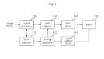
- FIG. 6 is a block diagram illustrating a construction of a controller shown in FIG. 7 .
- the controller 80 may include a signal processor 100, a flash memory 110, a timing controller 120, and a data aligner 130.
- the PDP device has a VSC board (not shown) which performs a signal process on an inputted image signal so that the image signal may be displayed on the plasma display panel, and supplies the processed signal to the controller.
- the VSC board (not shown) scales an inputted image signal according to the resolution of the plasma display panel.
- the signal processor 100 performs a predetermined signal process on the image signal inputted from the VSC board (not shown) to convert the image signal into data to be displayed.
- the signal process information for signal processing of the signal processor 100 are stored at the flash memory 110.
- the flash memory 110 may include EEPROM (Electrically Erasable and Programmable Read Only Memory).
- the timing controller 120 receives horizontal/vertical synchronization signals H and V to generate a timing control signal to control the driving period of the panel 160, and outputs the generated timing control signal to the data aligner 130 and scan/sustain driver 150 to control the timing of the driving signals supplied to the panel 160.
- the information associated with driving timing necessary to generate the timing control signal by the timing controller 120 for example, the duration of each period during which the panel 160 is separately driven, and the type of each period (type A or type B) are stored at the flash memory 110.
- the timing controller 120 receives the stored driving timing information from the flash memory 110 and generates the timing control signal using the received driving timing information and the horizontal/vertical synchronization signals H and V.
- the data aligner 130 receives the timing control signal generated from the timing controller 120 and the data processed by the signal processor 100 to align the data according to a scan order.
- the data driver 140 generates an address electrode driving signal using the aligned data and applies the generated address electrode driving signal to address electrodes (not shown) of the panel 160.
- the scan/sustain driver 150 generates a scan electrode driving signal and a sustain electrode driving signal using the timing controller inputted from the timing controller 120 and applies the generated driving signals to scan electrodes (not shown) and sustain electrodes (not shown) of the panel 160.
- the data aligner 130 may generate not only the aligned data signals but also a middle signal having information on whether two or more consecutive data out of the aligned data signals comply with each other, and transmit the generated aligned data signals and the middle signal to the data driver 140.
- the middle signal may be adapted to have any variation in signal value only in case that the consecutive data comply with each other, and the middle signal that has only the information on whether the data comply with each other may have less variation in signal value than that of a clock signal.
- switches included in the data driver 140 cause a high-rate switching operation by consecutive variation in signal value of the clock signal, and accordingly, power consumption and EMI may increase and margin for panel driving may decrease.
- a high resolution panel such as full HD panel needs to increase the clock frequency as the data to be displayed increase, and this may accelerate the increase of power consumption and EMI and the decrease of driving margin.
- the PDP device transmits the middle signal having small variation in signal value than that of the clock signal along with the data signals to reduce the occurrence of EMI and power consumption and ensure sufficient driving margin.
- the width of scan signal should be less than 1.1 us to ensure a driving margin of the panel.
- the width of the scan signal decreases, however, jitter characteristics are lowered, which may increase discharge delay in the address period.
- the width of scan signal is reduced to less than 0.7us, considerable discharge delay may take place due to lowering of jitter characteristics, and therefore, it can be possible to identify there is a wrong address discharge.
- FIG. 7 is a block diagram illustrating a construction of a plasma display panel according to an exemplary embodiment of the present invention.
- the controller 200 may include a middle signal generator that generates a middle signal according to a data signal to be transmitted to the data driver 210.
- the middle signal has information on whether two or more consecutive data comply with each other out of the data signals, and the controller 200 transmits the middle signal to the data driver 210 along with the data signal.
- the data signal may be a differential signal.
- the controller 200 may convert a data signal with TTL level (5V) into a low voltage differential signal with a level of 0.9V to 1.9V, for example 1.5V, and then serially transmit the converted low voltage differential signal.
- TTL level 5V
- Such converting into low voltage signal and transmitting may reduce noise and power consumption during transmission and such transmitting of the differential signal may reduce influence from common mode noise and EMI.
- the data driver 210 receives serially transmitted low voltage differential signal and converts the received low voltage differential signal back into the signal with TTL level (5V).
- the middle signal generator 201 compares two or more consecutive data out of the data signals to each other to determine if the two or more consecutive data comply with each other, and generates a middle signal having a signal value varying depending on whether the two or more consecutive data comply with each other.
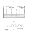
- FIG. 8 and FIG. 9 are views illustrating a method of generating a middle signal having information on whether two or more consecutive data comply with one another according to an exemplary embodiment of the present invention.
- the middle signal generator 201 changes the value of the middle signal. That is, in case that the current data is equal to the previous data and the value of the middle signal corresponding to the previous data is '0', the value of the middle signal corresponding to the current data becomes '1'.
- the middle signal generator 201 maintains the value of the middle signal. That is, in case that the current data is different from the previous data and the value of the middle signal corresponding to the previous data is '0', the value of the middle signal corresponding to the current data becomes '0'.
- the first middle signal value is initialized as '0', and if the data of a data signal changes from 1 to 0, the middle signal value maintains 0 and therefore the second middle signal value becomes 0. Then, while the data of the data signal changes continuously, the middle signal value maintains 0. As the fourth data and fifth data of the data signal maintain 0, the middle signal value changes from 0 to 1. Then while the data of the data signal changes continuously, the middle signal value maintains 1.
- the middle signal which is generated to have information on whether consecutive data out of data signals comply with each other, has very tiny change in signal value compared to the clock signal.
- the middle signal generator 201 determines the current middle signal value depending on whether the current data complies with the previous data and the previous middle signal value
- the present invention is not limited thereto.
- the middle signal generator 201 may determine the current middle signal value and generate the middle signal using three or more consecutive data and two or more previous middle signal values.
- the controller 200 transmits the middle signal generated in the above method along with the data signal to the data driver 210.
- the data driver 210 may include a clock generator 211 generating a clock signal using the data signal and middle signal transmitted from the controller 200.
- the clock generator 211 may generate a clock signal using the information on whether the consecutive data of the data signal included in the data signal and the middle signal comply with each other. A method of generating a clock signal by a clock generator 211 will be described with reference to FIG. 10 .
- the clock generator 211 may generate a clock signal from a data signal and a middle signal using a reverse-operation of an operation for generating a middle signal shown in FIG. 8 . That is, the clock generator 211 is adapted so that the clock signal value is a high level value, i.e. 1 in case that the data of the data signal is different from the middle signal value, and a low level value, i.e. 0 in case that the data of the data signal is equal to the middle signal value. Therefore, the clock generator 211 may generate a clock signal that varies continuously according to a predetermined frequency as shown in FIG. 10 .
- a shift register 212 extracts data to be supplied to each address electrode out of inputted data signals using the clock signal generated in the clock generator 212 and outputs the extracted data.
- the shift register 212 shifts all bits of the data signal to their next bits in accordance with the period of the generated clock signal, and therefore, a new bit of the data signal enters into an end of the bit stream and the previous last bit is out of the bit stream.
- the shift register 212 outputs data to be supplied to each of the plural address electrodes, and the data are converted in voltage level by plural level shifters 213, 214, and 215 and then supplied to each of the plural address electrodes.
- FIG. 10 is a view illustrating a method of generating a clock signal using a data signal and a middle signal.
- the controller 200 may transmit a control signal such as a strobe signal STB and a blanking signal BLK to the data driver 210 along with the data signal.
- a control signal such as a strobe signal STB and a blanking signal BLK
- the strobe signal STB is a signal to control the data output of the shift register 212.
- the shift register 212 outputs data in accordance with the generated clock, and in case that the strobe signal (STB) value is 0, the shift register 212 maintains the data not to be outputted.
- the clock generator 211 generates a clock signal using the data signal and the middle signal while the strobe signal (STB) value is maintained as 1, and outputs the generated clock signal to the shift register 212, and if the strobe signal (STB) value changes into 0, the clock generator 211 initializes the data signal and the middle signal as 0 and stops generating and outputting the clock signal.
- the strobe signal (STB) value is 1 and therefore data corresponding to each address electrode is outputted from the shift register 212 according to the clock signal generated by the clock generator 211.
- the strobe signal (STB) value changes into 0, the data signal value and the middle signal value are initialized as 0 and the clock generator 211 and the shift register 212 stop their operations.
- the reset period or address period may exist as described above with reference to FIG. 4 .
- the strobe signal (STB) value changes back to 1, and the clock generator 211 generates a clock signal and the shift register 212 outputs data according to the generated clock signal.
- the flat panel display device may reduce power consumption or EMI occurring due to high-rate switching operations and ensure a sufficient driving margin of a panel by transmitting a middle signal, variation in signal value of which is smaller than that of a clock signal, to the data driver along with a data signal.
Landscapes
- Engineering & Computer Science (AREA)
- Physics & Mathematics (AREA)
- Computer Hardware Design (AREA)
- General Physics & Mathematics (AREA)
- Theoretical Computer Science (AREA)
- Power Engineering (AREA)
- Plasma & Fusion (AREA)
- Control Of Indicators Other Than Cathode Ray Tubes (AREA)
- Control Of Gas Discharge Display Tubes (AREA)
Applications Claiming Priority (1)
| Application Number | Priority Date | Filing Date | Title |
|---|---|---|---|
| KR1020070053341A KR20080105579A (ko) | 2007-05-31 | 2007-05-31 | 플라즈마 디스플레이 장치 |
Publications (2)
| Publication Number | Publication Date |
|---|---|
| EP1998311A2 true EP1998311A2 (de) | 2008-12-03 |
| EP1998311A3 EP1998311A3 (de) | 2010-03-03 |
Family
ID=39743092
Family Applications (1)
| Application Number | Title | Priority Date | Filing Date |
|---|---|---|---|
| EP08157366A Withdrawn EP1998311A3 (de) | 2007-05-31 | 2008-05-30 | Anzeigevorrichtung mit Flachbildschirm |
Country Status (3)
| Country | Link |
|---|---|
| US (1) | US8120602B2 (de) |
| EP (1) | EP1998311A3 (de) |
| KR (1) | KR20080105579A (de) |
Cited By (1)
| Publication number | Priority date | Publication date | Assignee | Title |
|---|---|---|---|---|
| US11885735B2 (en) | 2019-09-13 | 2024-01-30 | Ethicon, Inc. | Ex vivo and in vivo systems for evaluating hemostatic patches, sealants, adhesives on solid organs |
Families Citing this family (2)
| Publication number | Priority date | Publication date | Assignee | Title |
|---|---|---|---|---|
| KR101999759B1 (ko) * | 2012-09-11 | 2019-07-16 | 삼성디스플레이 주식회사 | 유기전계발광 표시장치 및 그의 구동방법 |
| TWI676357B (zh) * | 2015-06-05 | 2019-11-01 | 美商蘭姆研究公司 | 配方組之執行同步系統與方法 |
Family Cites Families (8)
| Publication number | Priority date | Publication date | Assignee | Title |
|---|---|---|---|---|
| KR100333683B1 (ko) * | 1998-12-30 | 2002-06-20 | 박종섭 | 반도체장치의데이터스트로브신호발생기 |
| JP2001272948A (ja) * | 2000-03-23 | 2001-10-05 | Nec Corp | プラズマディスプレイパネルの駆動方法およびプラズマディスプレイ装置 |
| KR100706742B1 (ko) * | 2000-07-18 | 2007-04-11 | 삼성전자주식회사 | 평판 디스플레이 장치 |
| US6897842B2 (en) * | 2001-09-19 | 2005-05-24 | Intel Corporation | Nonlinearly mapping video date to pixel intensity while compensating for non-uniformities and degradations in a display |
| US6744280B2 (en) * | 2002-05-09 | 2004-06-01 | Texas Instruments Incorporated | Voltage output differential (VOD) correction circuit for differential drivers |
| US20060041613A1 (en) * | 2004-08-18 | 2006-02-23 | Fackelmayer Jonathan R O | Method and system for visual art distribution and presentation |
| KR100612504B1 (ko) * | 2005-03-03 | 2006-08-14 | 엘지전자 주식회사 | 플라즈마 디스플레이 패널의 구동 장치 |
| WO2007013718A1 (en) * | 2005-07-28 | 2007-02-01 | Anapass Inc. | Clock signal embedded multi-level signaling method and apparatus for driving display panel using the same |
-
2007
- 2007-05-31 KR KR1020070053341A patent/KR20080105579A/ko not_active Withdrawn
-
2008
- 2008-05-30 EP EP08157366A patent/EP1998311A3/de not_active Withdrawn
- 2008-05-30 US US12/130,293 patent/US8120602B2/en not_active Expired - Fee Related
Cited By (1)
| Publication number | Priority date | Publication date | Assignee | Title |
|---|---|---|---|---|
| US11885735B2 (en) | 2019-09-13 | 2024-01-30 | Ethicon, Inc. | Ex vivo and in vivo systems for evaluating hemostatic patches, sealants, adhesives on solid organs |
Also Published As
| Publication number | Publication date |
|---|---|
| KR20080105579A (ko) | 2008-12-04 |
| EP1998311A3 (de) | 2010-03-03 |
| US8120602B2 (en) | 2012-02-21 |
| US20080297445A1 (en) | 2008-12-04 |
Similar Documents
| Publication | Publication Date | Title |
|---|---|---|
| EP1630775A1 (de) | Plasma-Anzeigetafel und Verfahren zur Steuerung derselben | |
| US8120602B2 (en) | Flat panel display with clock being generated insider the data driver using XOR logic with the data signal and a second signal generated from the data signal using a encoding scheme as the two inputs that are transmitted to a clock generator inside the data driver | |
| KR20060024215A (ko) | 플라즈마 디스플레이 패널의 데이터 제어방법 및 장치 | |
| CN100541573C (zh) | 等离子显示装置 | |
| CN100444222C (zh) | 等离子显示屏数据驱动器、驱动方法和等离子显示设备 | |
| EP2079071B1 (de) | Plasmaanzeigevorrichtung und Verfahren zu ihrer Ansteuerung | |
| KR20090057720A (ko) | 플라즈마 디스플레이 장치 | |
| KR100822215B1 (ko) | 디스플레이 패널의 구동장치 | |
| CN101542566B (zh) | 等离子体显示装置 | |
| US20050168408A1 (en) | Plasma display panel and driving method thereof | |
| KR100903647B1 (ko) | 플라즈마 디스플레이 패널 구동 장치 및 그를 이용한플라즈마 디스플레이 장치 | |
| US20090189885A1 (en) | Plasma display panel and method and device for driving the same | |
| EP1598799A2 (de) | Plasmaanzeigetafel und Treiberverfahren dafür | |
| US20050110708A1 (en) | Plasma display panel and driving method thereof | |
| US20080007489A1 (en) | Apparatus for driving plasma display panel | |
| KR20090047222A (ko) | 플라즈마 디스플레이 패널의 구동 방법 및 그를 이용한플라즈마 디스플레이 장치 | |
| US7158100B2 (en) | Driving apparatus for display panel | |
| KR100342832B1 (ko) | 플라즈마 디스플레이 패널의 구동장치 | |
| US7619586B2 (en) | Plasma display apparatus and method for driving the same | |
| KR100524315B1 (ko) | 플라즈마 디스플레이 패널의 구동장치와 그의 구동방법 | |
| US20060208970A1 (en) | Plasma display apparatus and driving method thereof | |
| KR20050051363A (ko) | 플라즈마 디스플레이 패널의 구동 방법 및 플라즈마 표시장치 | |
| KR20100033802A (ko) | 플라즈마 디스플레이 장치 | |
| KR20090048070A (ko) | 플라즈마 디스플레이 장치 | |
| KR20090049846A (ko) | 플라즈마 디스플레이 패널의 구동 방법 및 그를 이용한플라즈마 디스플레이 장치 |
Legal Events
| Date | Code | Title | Description |
|---|---|---|---|
| PUAI | Public reference made under article 153(3) epc to a published international application that has entered the european phase |
Free format text: ORIGINAL CODE: 0009012 |
|
| 17P | Request for examination filed |
Effective date: 20080530 |
|
| AK | Designated contracting states |
Kind code of ref document: A2 Designated state(s): AT BE BG CH CY CZ DE DK EE ES FI FR GB GR HR HU IE IS IT LI LT LU LV MC MT NL NO PL PT RO SE SI SK TR |
|
| AX | Request for extension of the european patent |
Extension state: AL BA MK RS |
|
| PUAL | Search report despatched |
Free format text: ORIGINAL CODE: 0009013 |
|
| AK | Designated contracting states |
Kind code of ref document: A3 Designated state(s): AT BE BG CH CY CZ DE DK EE ES FI FR GB GR HR HU IE IS IT LI LT LU LV MC MT NL NO PL PT RO SE SI SK TR |
|
| AX | Request for extension of the european patent |
Extension state: AL BA MK RS |
|
| RIC1 | Information provided on ipc code assigned before grant |
Ipc: G09G 3/20 20060101ALI20100125BHEP Ipc: G09G 3/28 20060101AFI20080922BHEP |
|
| AKX | Designation fees paid |
Designated state(s): DE FR GB NL |
|
| STAA | Information on the status of an ep patent application or granted ep patent |
Free format text: STATUS: THE APPLICATION IS DEEMED TO BE WITHDRAWN |
|
| 18D | Application deemed to be withdrawn |
Effective date: 20121201 |