EP2000793A2 - Microstructures, method for producing microstructures, and optical field amplifying device - Google Patents
Microstructures, method for producing microstructures, and optical field amplifying device Download PDFInfo
- Publication number
- EP2000793A2 EP2000793A2 EP08010356A EP08010356A EP2000793A2 EP 2000793 A2 EP2000793 A2 EP 2000793A2 EP 08010356 A EP08010356 A EP 08010356A EP 08010356 A EP08010356 A EP 08010356A EP 2000793 A2 EP2000793 A2 EP 2000793A2
- Authority
- EP
- European Patent Office
- Prior art keywords
- microstructure
- fine holes
- base material
- dielectric base
- local plasmon
- Prior art date
- Legal status (The legal status is an assumption and is not a legal conclusion. Google has not performed a legal analysis and makes no representation as to the accuracy of the status listed.)
- Withdrawn
Links
- 238000004519 manufacturing process Methods 0.000 title claims abstract description 11
- 230000003287 optical effect Effects 0.000 title claims description 50
- 229910052751 metal Inorganic materials 0.000 claims abstract description 83
- 239000002184 metal Substances 0.000 claims abstract description 83
- 239000000463 material Substances 0.000 claims abstract description 81
- 230000005684 electric field Effects 0.000 claims abstract description 54
- 230000003321 amplification Effects 0.000 claims abstract description 36
- 230000000694 effects Effects 0.000 claims abstract description 36
- 238000003199 nucleic acid amplification method Methods 0.000 claims abstract description 36
- 238000000034 method Methods 0.000 claims abstract description 25
- 230000001939 inductive effect Effects 0.000 claims abstract description 23
- 230000008569 process Effects 0.000 claims abstract description 14
- 238000007747 plating Methods 0.000 claims description 21
- 238000001069 Raman spectroscopy Methods 0.000 claims description 17
- 239000007769 metal material Substances 0.000 claims description 17
- 238000007743 anodising Methods 0.000 claims description 12
- 238000010521 absorption reaction Methods 0.000 claims description 10
- 239000003550 marker Substances 0.000 claims description 9
- 239000013076 target substance Substances 0.000 claims description 8
- 238000004949 mass spectrometry Methods 0.000 claims description 6
- 229910044991 metal oxide Inorganic materials 0.000 claims description 5
- 150000004706 metal oxides Chemical class 0.000 claims description 5
- 239000000370 acceptor Substances 0.000 claims description 3
- 230000000704 physical effect Effects 0.000 claims description 3
- 238000009826 distribution Methods 0.000 claims description 2
- 239000004020 conductor Substances 0.000 abstract description 17
- 238000012546 transfer Methods 0.000 description 14
- 238000002048 anodisation reaction Methods 0.000 description 12
- PNEYBMLMFCGWSK-UHFFFAOYSA-N aluminium oxide Inorganic materials [O-2].[O-2].[O-2].[Al+3].[Al+3] PNEYBMLMFCGWSK-UHFFFAOYSA-N 0.000 description 11
- 239000010410 layer Substances 0.000 description 10
- 230000000052 comparative effect Effects 0.000 description 9
- 238000010276 construction Methods 0.000 description 8
- 239000010931 gold Substances 0.000 description 8
- 239000002923 metal particle Substances 0.000 description 7
- MUBZPKHOEPUJKR-UHFFFAOYSA-N Oxalic acid Chemical compound OC(=O)C(O)=O MUBZPKHOEPUJKR-UHFFFAOYSA-N 0.000 description 6
- 229910052782 aluminium Inorganic materials 0.000 description 6
- XAGFODPZIPBFFR-UHFFFAOYSA-N aluminium Chemical compound [Al] XAGFODPZIPBFFR-UHFFFAOYSA-N 0.000 description 6
- 238000009713 electroplating Methods 0.000 description 6
- 150000002739 metals Chemical class 0.000 description 6
- 239000000758 substrate Substances 0.000 description 6
- 238000001237 Raman spectrum Methods 0.000 description 5
- 238000006243 chemical reaction Methods 0.000 description 5
- 239000008151 electrolyte solution Substances 0.000 description 5
- 229910052737 gold Inorganic materials 0.000 description 5
- 238000001514 detection method Methods 0.000 description 4
- 230000005284 excitation Effects 0.000 description 4
- 239000000243 solution Substances 0.000 description 4
- 238000004577 artificial photosynthesis Methods 0.000 description 3
- VYXSBFYARXAAKO-WTKGSRSZSA-N chembl402140 Chemical compound Cl.C1=2C=C(C)C(NCC)=CC=2OC2=C\C(=N/CC)C(C)=CC2=C1C1=CC=CC=C1C(=O)OCC VYXSBFYARXAAKO-WTKGSRSZSA-N 0.000 description 3
- 239000011521 glass Substances 0.000 description 3
- PCHJSUWPFVWCPO-UHFFFAOYSA-N gold Chemical compound [Au] PCHJSUWPFVWCPO-UHFFFAOYSA-N 0.000 description 3
- 230000001965 increasing effect Effects 0.000 description 3
- 239000002105 nanoparticle Substances 0.000 description 3
- 230000035945 sensitivity Effects 0.000 description 3
- 238000007740 vapor deposition Methods 0.000 description 3
- NBIIXXVUZAFLBC-UHFFFAOYSA-N Phosphoric acid Chemical compound OP(O)(O)=O NBIIXXVUZAFLBC-UHFFFAOYSA-N 0.000 description 2
- QAOWNCQODCNURD-UHFFFAOYSA-N Sulfuric acid Chemical compound OS(O)(=O)=O QAOWNCQODCNURD-UHFFFAOYSA-N 0.000 description 2
- 238000002679 ablation Methods 0.000 description 2
- 238000013461 design Methods 0.000 description 2
- 238000010894 electron beam technology Methods 0.000 description 2
- 239000012530 fluid Substances 0.000 description 2
- 239000003574 free electron Substances 0.000 description 2
- 238000005259 measurement Methods 0.000 description 2
- 235000006408 oxalic acid Nutrition 0.000 description 2
- 230000029553 photosynthesis Effects 0.000 description 2
- 238000010672 photosynthesis Methods 0.000 description 2
- 238000000926 separation method Methods 0.000 description 2
- 229910052709 silver Inorganic materials 0.000 description 2
- 229910052719 titanium Inorganic materials 0.000 description 2
- RHQQHZQUAMFINJ-GKWSUJDHSA-N 1-[(3s,5s,8s,9s,10s,11s,13s,14s,17s)-3,11-dihydroxy-10,13-dimethyl-2,3,4,5,6,7,8,9,11,12,14,15,16,17-tetradecahydro-1h-cyclopenta[a]phenanthren-17-yl]-2-hydroxyethanone Chemical compound C1[C@@H](O)CC[C@]2(C)[C@H]3[C@@H](O)C[C@](C)([C@H](CC4)C(=O)CO)[C@@H]4[C@@H]3CC[C@H]21 RHQQHZQUAMFINJ-GKWSUJDHSA-N 0.000 description 1
- LSNNMFCWUKXFEE-UHFFFAOYSA-M Bisulfite Chemical compound OS([O-])=O LSNNMFCWUKXFEE-UHFFFAOYSA-M 0.000 description 1
- OKTJSMMVPCPJKN-UHFFFAOYSA-N Carbon Chemical compound [C] OKTJSMMVPCPJKN-UHFFFAOYSA-N 0.000 description 1
- 229910001111 Fine metal Inorganic materials 0.000 description 1
- UFHFLCQGNIYNRP-UHFFFAOYSA-N Hydrogen Chemical compound [H][H] UFHFLCQGNIYNRP-UHFFFAOYSA-N 0.000 description 1
- 239000002253 acid Substances 0.000 description 1
- 230000002378 acidificating effect Effects 0.000 description 1
- 229910000147 aluminium phosphate Inorganic materials 0.000 description 1
- 150000001408 amides Chemical class 0.000 description 1
- 238000000137 annealing Methods 0.000 description 1
- SRSXLGNVWSONIS-UHFFFAOYSA-N benzenesulfonic acid Chemical compound OS(=O)(=O)C1=CC=CC=C1 SRSXLGNVWSONIS-UHFFFAOYSA-N 0.000 description 1
- 229940092714 benzenesulfonic acid Drugs 0.000 description 1
- 230000015572 biosynthetic process Effects 0.000 description 1
- 229910052799 carbon Inorganic materials 0.000 description 1
- 230000008859 change Effects 0.000 description 1
- KRVSOGSZCMJSLX-UHFFFAOYSA-L chromic acid Substances O[Cr](O)(=O)=O KRVSOGSZCMJSLX-UHFFFAOYSA-L 0.000 description 1
- 229910052802 copper Inorganic materials 0.000 description 1
- 229910052593 corundum Inorganic materials 0.000 description 1
- 238000011161 development Methods 0.000 description 1
- 238000010586 diagram Methods 0.000 description 1
- 230000002708 enhancing effect Effects 0.000 description 1
- 238000011156 evaluation Methods 0.000 description 1
- 230000008020 evaporation Effects 0.000 description 1
- 238000001704 evaporation Methods 0.000 description 1
- 230000002349 favourable effect Effects 0.000 description 1
- 239000002803 fossil fuel Substances 0.000 description 1
- AWJWCTOOIBYHON-UHFFFAOYSA-N furo[3,4-b]pyrazine-5,7-dione Chemical compound C1=CN=C2C(=O)OC(=O)C2=N1 AWJWCTOOIBYHON-UHFFFAOYSA-N 0.000 description 1
- 229910052735 hafnium Inorganic materials 0.000 description 1
- 229910052739 hydrogen Inorganic materials 0.000 description 1
- 239000001257 hydrogen Substances 0.000 description 1
- 239000012535 impurity Substances 0.000 description 1
- 229910052738 indium Inorganic materials 0.000 description 1
- AMGQUBHHOARCQH-UHFFFAOYSA-N indium;oxotin Chemical compound [In].[Sn]=O AMGQUBHHOARCQH-UHFFFAOYSA-N 0.000 description 1
- 238000010884 ion-beam technique Methods 0.000 description 1
- 230000031700 light absorption Effects 0.000 description 1
- 238000001459 lithography Methods 0.000 description 1
- 238000012986 modification Methods 0.000 description 1
- 230000004048 modification Effects 0.000 description 1
- LNOPIUAQISRISI-UHFFFAOYSA-N n'-hydroxy-2-propan-2-ylsulfonylethanimidamide Chemical compound CC(C)S(=O)(=O)CC(N)=NO LNOPIUAQISRISI-UHFFFAOYSA-N 0.000 description 1
- 229910052759 nickel Inorganic materials 0.000 description 1
- 230000010355 oscillation Effects 0.000 description 1
- 238000007254 oxidation reaction Methods 0.000 description 1
- 229910052697 platinum Inorganic materials 0.000 description 1
- 238000002360 preparation method Methods 0.000 description 1
- 239000002096 quantum dot Substances 0.000 description 1
- 239000011347 resin Substances 0.000 description 1
- 229920005989 resin Polymers 0.000 description 1
- 239000002094 self assembled monolayer Substances 0.000 description 1
- 239000013545 self-assembled monolayer Substances 0.000 description 1
- 239000004065 semiconductor Substances 0.000 description 1
- 229910052710 silicon Inorganic materials 0.000 description 1
- 239000002356 single layer Substances 0.000 description 1
- 238000002791 soaking Methods 0.000 description 1
- 230000003595 spectral effect Effects 0.000 description 1
- 239000000126 substance Substances 0.000 description 1
- 229910052715 tantalum Inorganic materials 0.000 description 1
- 230000007704 transition Effects 0.000 description 1
- 230000000007 visual effect Effects 0.000 description 1
- 229910001845 yogo sapphire Inorganic materials 0.000 description 1
- 229910052725 zinc Inorganic materials 0.000 description 1
- 229910052726 zirconium Inorganic materials 0.000 description 1
Images



Classifications
-
- G—PHYSICS
- G01—MEASURING; TESTING
- G01N—INVESTIGATING OR ANALYSING MATERIALS BY DETERMINING THEIR CHEMICAL OR PHYSICAL PROPERTIES
- G01N21/00—Investigating or analysing materials by the use of optical means, i.e. using sub-millimetre waves, infrared, visible or ultraviolet light
- G01N21/17—Systems in which incident light is modified in accordance with the properties of the material investigated
- G01N21/55—Specular reflectivity
- G01N21/552—Attenuated total reflection
- G01N21/553—Attenuated total reflection and using surface plasmons
- G01N21/554—Attenuated total reflection and using surface plasmons detecting the surface plasmon resonance of nanostructured metals, e.g. localised surface plasmon resonance
-
- G—PHYSICS
- G01—MEASURING; TESTING
- G01N—INVESTIGATING OR ANALYSING MATERIALS BY DETERMINING THEIR CHEMICAL OR PHYSICAL PROPERTIES
- G01N21/00—Investigating or analysing materials by the use of optical means, i.e. using sub-millimetre waves, infrared, visible or ultraviolet light
- G01N21/62—Systems in which the material investigated is excited whereby it emits light or causes a change in wavelength of the incident light
- G01N21/63—Systems in which the material investigated is excited whereby it emits light or causes a change in wavelength of the incident light optically excited
- G01N21/64—Fluorescence; Phosphorescence
- G01N21/6428—Measuring fluorescence of fluorescent products of reactions or of fluorochrome labelled reactive substances, e.g. measuring quenching effects, using measuring "optrodes"
-
- G—PHYSICS
- G01—MEASURING; TESTING
- G01N—INVESTIGATING OR ANALYSING MATERIALS BY DETERMINING THEIR CHEMICAL OR PHYSICAL PROPERTIES
- G01N21/00—Investigating or analysing materials by the use of optical means, i.e. using sub-millimetre waves, infrared, visible or ultraviolet light
- G01N21/62—Systems in which the material investigated is excited whereby it emits light or causes a change in wavelength of the incident light
- G01N21/63—Systems in which the material investigated is excited whereby it emits light or causes a change in wavelength of the incident light optically excited
- G01N21/64—Fluorescence; Phosphorescence
- G01N21/645—Specially adapted constructive features of fluorimeters
- G01N21/648—Specially adapted constructive features of fluorimeters using evanescent coupling or surface plasmon coupling for the excitation of fluorescence
-
- G—PHYSICS
- G01—MEASURING; TESTING
- G01N—INVESTIGATING OR ANALYSING MATERIALS BY DETERMINING THEIR CHEMICAL OR PHYSICAL PROPERTIES
- G01N21/00—Investigating or analysing materials by the use of optical means, i.e. using sub-millimetre waves, infrared, visible or ultraviolet light
- G01N21/62—Systems in which the material investigated is excited whereby it emits light or causes a change in wavelength of the incident light
- G01N21/63—Systems in which the material investigated is excited whereby it emits light or causes a change in wavelength of the incident light optically excited
- G01N21/65—Raman scattering
- G01N21/658—Raman scattering enhancement Raman, e.g. surface plasmons
-
- Y—GENERAL TAGGING OF NEW TECHNOLOGICAL DEVELOPMENTS; GENERAL TAGGING OF CROSS-SECTIONAL TECHNOLOGIES SPANNING OVER SEVERAL SECTIONS OF THE IPC; TECHNICAL SUBJECTS COVERED BY FORMER USPC CROSS-REFERENCE ART COLLECTIONS [XRACs] AND DIGESTS
- Y10—TECHNICAL SUBJECTS COVERED BY FORMER USPC
- Y10T—TECHNICAL SUBJECTS COVERED BY FORMER US CLASSIFICATION
- Y10T428/00—Stock material or miscellaneous articles
- Y10T428/24—Structurally defined web or sheet [e.g., overall dimension, etc.]
- Y10T428/24273—Structurally defined web or sheet [e.g., overall dimension, etc.] including aperture
- Y10T428/24322—Composite web or sheet
- Y10T428/24331—Composite web or sheet including nonapertured component
Definitions
- the present invention relates to a microstructure equipped with a dielectric base material having a plurality of fine holes in the surface thereof and metal members capable of inducing local plasmon, a method for producing the microstructure, and an optical field amplifying device that utilizes the microstructure.
- Light energy transfer elements that efficiently utilize solar energy, are being considered. Solar energy is being investigated as a new, clean, and safe alternative energy source to replace fossil fuels such as oil.
- the photosynthesis function of plants has been noted as a highly efficient method of light energy transfer, and there is expectation for development of artificial light energy transfer elements (artificial photosynthesis elements) equipped with artificially constructed photosystem complexes that have photosynthesis functions.
- Japanese Unexamined Patent Publication Nos. 2001-303022 and 2002-25635 disclose light energy transfer elements (photoelectric conversion systems). These light energy transfer elements are equipped with: a metal or semiconductor base material; and a mixed self assembled monolayer. These light energy transfer elements are easy to produce, and light which is absorbed by the complex can be highly efficiently converted to energy. However, because the film thickness of the monolayer is several nm, the absorption efficiency of incident light is extremely low.
- Japanese Unexamined Patent Publication No. 2005-259674 discloses a photoelectric conversion element.
- photoelectric conversion element photosystem complexes are formed on a microstructure constituted by electrodes which are formed by accumulated gold nanoparticles.
- the high specific surface area of the gold nanoparticles and an electric field amplifying effect caused by local plasmon enables highly efficient photoelectric conversion of incident light, by photosystem complexes which are immobilized on the electrodes at high density.
- Japanese Unexamined Patent Publication No. 2004-530867 discloses an optical amplifying substance, in which a plurality of agglomerated nanoparticles (including fractals) are provided in the vicinity of microcavities, as a microstructure having an electric field amplifying effect.
- U.S. Patent No. 7,288,419 discloses a microstructure equipped with a dielectric base material and a plurality of fine metal particles. In this microstructure, highly densely arranged fine holes are provided in the surface of the dielectric base material, and each of the metal particles includes a filling portion that fills a fine hole, and a head portion that protrudes from the surface of the dielectric base material and which are of a size capable of inducing local plasmon resonance.
- the present invention has been developed in view of the foregoing circumstances. It is an object of the present invention to provide a microstructure that exhibits electric field amplification effects having high planar uniformity and which can be produced by a simple process.
- the microstructure may be employed as an optical field amplifying device, for a light energy transfer element or the like. It is another object of the present invention to provide a method for manufacturing the microstructure.
- a first microstructure of the present invention comprises:
- the term "great number” is defined as a number far greater than the number of fine holes which are filled by the filling portions.
- the "diameter" of the protruding portion is defined as the maximum diameter thereof.
- a second microstructure of the present invention comprises:
- the average distance between adjacent protruding portions is 10nm or less.
- distance refers to the distance between the closest portions of separate and adjacent protruding portions.
- the distribution of the fine holes within the dielectric base material is preferable for the distribution of the fine holes within the dielectric base material to be substantially regular.
- the dielectric base material prefferably be formed by a metal oxide which is obtained by anodizing at least a portion of a metallic material, and for the fine holes to be formed within the metal oxide during the anodizing process.
- the micro metal members may be formed by plating the interiors of the fine holes formed in the dielectric base material until a portion of the plating protrudes from the surface of the dielectric base material.
- An optical field amplifying device of the present invention is equipped with the microstructure of the present invention, and is characterized by:
- a preferred example of the optical field amplifying device of the present invention has a sample placed in contact with an electric field amplification region created by the local plasmon on the surface thereof; and a measuring light beam that enters the sample is emitted as emitted light beams having different physical properties, depending on the sample.
- optical field amplifying device of the present invention has a sample placed in contact with an electric field amplification region created by the local plasmon on the surface of the optical amplifying device; and Raman scattered light is generated by a measuring light beam of a specific wavelength entering the sample.
- Still another preferred example of the optical field amplifying device of the present invention has a target placed in contact with an electric field amplification region created by the local plasmon on the surface of the optical amplifying device; a laser beam is irradiated onto the target; and the portion of the target irradiated by the laser beam is caused to transpire.
- Still yet another preferred example of the optical field amplifying device of the present invention has a sample placed in contact with an electric field amplification region created by the local plasmon on the surface of the optical amplifying device; and a measuring light beam is irradiated onto the sample, to desorb a target of mass spectrometry, which is included in the sample, from the surface.
- a method for producing a microstructure capable of inducing local plasmon on the surface thereof of the present invention comprises the steps of:
- each of the plurality of micro metal members have a filling portion that fills one or more of the fine holes and a protruding portion that protrudes from the surface of the base material.
- Each of the protruding portions 22 is of a diameter, which is greater than the diameter of the filling portion and capable of inducing local plasmon. Therefore, the head portions can be provided close to each other, and effective electric field amplification functions can be obtained.
- the micro metal members are of structures wherein portions thereof are embedded in the fine holes of the dielectric base material. Therefore, the micro metal members are not likely to flake off from the dielectric base material, and an electric field amplification effect having high planar uniformity is exhibited. Further, the micro metal members include those of which the filling portions fill a plurality of the fine holes. Accordingly, strict control of the production process is obviated, that is, the micro metal members can be produced by a simple process.
- the micro metal members include those that have different numbers of filling portions that fill different numbers of the fine holes.
- the sizes of the protruding portions become non uniform.
- the wavelength at which an electric field amplifying effect due to local plasmon can be obtained varies according to the type of metal and the size thereof. Therefore, the first microstructure of the present invention, in which the sizes of the protruding portions are not uniform, the wavelengths at which the electric field amplification effect can be obtained are broadened, corresponding to the fluctuation in the sizes of the protruding portions.
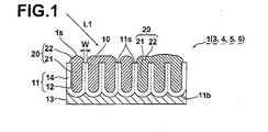
- FIG. 1 is a sectional view that illustrates the construction of the microstructure 1.
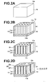
- Figure 2 and Figure 3 are diagrams that illustrate the manufacturing steps of the microstructure according to the first embodiment, wherein Figure 2 shows perspective views of each step, and Figure 3 shows sectional views of each step.
- the microstructure 1 is formed on a conductor 13, and is equipped with a dielectric base material 11 with a great number of regularly arranged fine holes 12, which are substantially the same shape in plan view, formed such that they are open at the surface 11s of the dielectric base material 11.
- a plurality of micro metal members 20, each of which have a filling portion 21 that fills one or more of the fine holes 12 and a protruding portion 22 that protrudes from the surface 11s of the base material 11 and is of a diameter, which is greater than the diameter of the filling portion, capable of inducing local plasmon, are fixed to the dielectric base material 11.
- the plurality of micro metal members 20 include those that have different numbers of filling portions 21 that fill different numbers of the fine holes 12.
- An incident light beam L1 that includes wavelengths of light capable of inducing local plasmon at the protruding portions 22 is irradiated onto the surface 11s of the dielectric base material 11 of the microstructure 1.
- the incident light beam L1 is not particularly limited, and may be natural light, such as sunlight, a light beam emitted by a specific light source, or a broad wavelength band light beam.
- the incident light beam L1 causes Local plasmon to be induced at the protruding portions 22 of the microstructure 1, and an electric field amplifying effect is obtained due to the local plasmon.
- the electric field amplification effect due to local plasmon is said to be a hundredfold or greater at the local plasmon resonance wavelength. Accordingly, it is preferable for the incident light beam L1 to include a wavelength of light that causes local plasmon resonance at the protruding portions 22, in order to obtain greater electric field amplification effects.
- the fine holes 12 extend substantially straight in the thickness direction of the microstructure 1 from the surface 11s of the dielectric base material 11.
- the fine holes 12 are closed at the bottom surface 11b of the dielectric base material 11, and do not penetrate therethrough.
- the dielectric base material 11 is an alumina (Al 2 O 3 ) layer 11 (metal oxide layer) which is obtained by partially anodizing a metal material 10 having aluminum (Al) as its main component and which may have slight impurities contained therein, as illustrated in Figure 2 and Figure 3 .
- the fine holes 12 are formed as holes having rounded bottoms during the partial anodizing process. The remaining non anodized portion of the metal material 10 becomes the conductor 13.
- the shape of the metal material 10 to be anodized is not limited.
- a metal plate is an example.
- the metal material 10 may be formed as a layer on a substrate.
- Anodization may be executed by using the metal material 10 as an anode, using carbon, aluminum, or the like as a cathode (opposing electrode), soaking the anode and the cathode in an anodizing electrolytic solution, then applying voltage therebetween.
- the electrolytic solution is not particularly limited. Acidic electrolytic solutions that include at least one of: sulfuric acid; phosphoric acid; chromic acid; oxalic acid; sulfamic acid; benzene sulfonic acid; amide sulfonic acid; and the like may be favorably employed.
- an oxidation reaction progresses substantially in the vertical direction from the surface 10s thereof (the upper surface in the Figures) as illustrated in Figure 2B and Figure 3B , to form the alumina layer 11.
- the alumina layer 11 formed by anodization is of a structure in which fine columns 14 which are substantially hexagonal in plan view are arranged adjacent to each other.
- the fine holes 12 that extend in the depth direction from the surface 10s are formed at the approximate centers of each of the fine columns 14.
- the bottom surfaces of the fine holes 12 and the fine columns 14 are rounded in shape, as illustrated in Figure 2 and Figure 3 .
- the structure of alumina layers which are formed by anodization is described in H. Masuda, "Preparation of Mesoporous Alumina and Applications as a Functional Material", Material Science, pp. 34, Vol. 15, No. 10, 1997 .
- partial anodization is performed on the metal material 10.
- oxalic acid employed as the electrolytic solution
- an example of favorable anodization conditions are: an electrolytic solution concentration of 0.5M; a solution temperature of 15°C; and an applied voltage of 40V.
- the pitch among adjacent fine holes 12 can be controlled to be within a range of 10nm to 500nm.
- the diameters of the fine holes 12 can be controlled to be within a range of 5nm to 400nm.
- Japanese Unexamined Patent Publication Nos. 2001-9800 and 2001-138300 disclose methods for exerting detailed control on the positions and the diameters of fine holes when forming the fine holes. Fine holes can be regularly arranged and formed with desired diameters and depths within the aforementioned ranges, by employing these methods.
- the micro metal members 20, which are constituted by the filling portions 21 and the protruding portions 22, are formed by administering electroplating within the fine holes 12 of the dielectric base material 11, as illustrated in Figure 2C and Figure 3C .
- the anodized alumina layer 11 is present between the conductor 13 and the bottoms of the fine holes 12.
- electroplating using the conductor 13 as an electrode enables prioritized separation of the metal from the bottoms of the fine holes 12, where electric fields are powerful.
- Electroplating using the conductor 13 as an electrode enables prioritized separation of the metal from the bottoms of the fine holes 12, where electric fields are powerful. Therefore, by continuously performing electroplating, the metal fills the interiors of the fine holes 12, to form the filling portions 21 of the micro metal members 20. When electroplating is continued after the filling portions 21 are formed, the metal overflows from the fine holes 12. However, because electric fields are powerful in the vicinities of the fine holes 12, the metal that overflows is isotropically plated at the peripheries of the fine holes 12.
- the metal which is plated at the peripheries of the fine holes 12 protrude from the surface 11s of the dielectric base material 11 above the filling portions 21, and become the protruding portions 22 which have diameters greater than those of the filling portions 21 (refer to Figure 2D and Figure 3D ).
- the microstructure 1 is equipped with micro metal members 20 having filling portions 21 that fill different numbers of the fine holes 12.
- the sizes of the protruding portions 22 of the micro metal members 20 change according to the number of fine holes 12 which are filled by the filling portions 21 thereof. For example, in the case that the fine holes 12 which have substantially uniform diameters are arranged substantially regularly, if the number of fine holes 12 filled by the filling portion 21 is doubled, the size of the protruding portion 22 is approximately doubled.
- microstructure 1 of the first embodiment is equipped with micro metal members 20 having filling portions 21 that fill different numbers of the fine holes 12. Therefore, it is not necessary to strictly control the plating conditions. Accordingly, the microstructure 1 can be produced by a simple process.
- the wavelength at which local plasmon resonance wavelength occurs varies according to the type of metal and the size thereof. Accordingly, if there are fluctuations in the number of fine holes 12 which are filled by the filing portions 21, the sizes of the protruding portions 22 that induce local plasmon also fluctuate. As a result, the wavelengths at which local plasmon can be induced are broadened, corresponding to the fluctuation in the sizes of the protruding portions 22.
- the number of fine holes 12 which are filled by the filling portions 21 can be adjusted by the plating conditions when forming the protruding portions 22. Therefore, the wavelength or the wavelength range at which local plasmon is induced can be varied by changing the plating conditions. If plating is continued after a protruding portion 22 is formed on a filling portion 21 that fills a single fine hole 12, adjacent protruding portions 22 contact each other and become integrated. As a result, single protruding portions 22 which are formed by two protruding portions 22 and micro metal members 22 which are formed by two filling portions 21 that fill two fine holes 12 can be formed. The sizes of the protruding portions 22 can be varied by adjusting the number of protruding portions 22 to be integrated, by the simple process of merely changing the plating conditions.
- the size of the protruding portions 22 is large enough to induce local plasmon, there is no limitation on the number of fine holes 12 which are filled by the filling portions 21. From the viewpoint of broadening the wavelength band at which local plasmon resonance can be induced, it is preferable for the microstructure 1 to include micro metal members 20 having filling portions 21 that fill single fine holes 12. Taking the wavelength and the like of the incident light beam L1 into consideration, it is preferable for the sizes of the protruding portions 22 to be within a range of 10nm to 300nm. Protruding portions 22 of sizes within this range are capable of inducing local plasmon with light beams within a wavelength range from 300nm to near infrared.
- adjacent protruding portions 22 it is preferable for adjacent protruding portions 22 to be separated. It is preferable for the average value of distances w among adjacent protruding portions 22 to be within a range of several nm to 10nm. Electric field amplification effects are known to be particularly powerful when the distance w is 10nm or less. Accordingly, if the average value of the distances w is within the aforementioned range, an electric field amplification effect due to local plasmon can be effectively obtained.
- the micro metal members 20 may be any metal that has free electrons.
- the microstructure 1 induces local plasmon at the protruding portions 22 when the incident light beam L1 is irradiated onto the surface 11s of the dielectric base material. Therefore, metals that generate local plasmon are preferred as materials for the micro metal members 20. Examples of such materials are Au, Ag, Cu, Pt, Ni, and Ti. Au and Ag, which have high electric field amplification effects, are particularly preferable.
- the microstructure illustrated in Figure 2D and Figure 3D are capable of effectively generating electrical field amplification effects due to local plasmon at the protruding portions 22.
- each of the micro metal members 20 have a filling portion 21 that fills one or more of the fine holes 12 and a protruding portion 22 that protrudes from the surface 11s of the dielectric base material 11.
- Each of the protruding portions 22 is of a diameter, which is greater than the diameter of the filling portions 21 and capable of inducing local plasmon. Therefore, the head portions can be provided close to each other, and effective electric field amplification functions can be obtained.
- the micro metal members 20 are of structures wherein portions thereof are embedded in the fine holes 12 of the dielectric base material 11. Therefore, the micro metal members 20 are not likely to flake off from the dielectric base material 11, and an electric field amplification effect having high planar uniformity is exhibited. Further, the micro metal members 20 include those of which the filling portions 21 fill a plurality of the fine holes 12. Accordingly, strict control of the production process is obviated, that is, the micro metal members 20 can be produced by a simple process.
- the micro metal members 20 include those that have different numbers of filling portions 21 that fill different numbers of the fine holes 12.
- the sizes of the protruding portions 22 become non uniform.
- the wavelength at which an electric field amplifying effect due to local plasmon can be obtained varies according to the type of metal and the size thereof. Therefore, the microstructure 1, in which the sizes of the protruding portions 22 are not uniform, the wavelengths at which the electric field amplification effect can be obtained are broadened, corresponding to the fluctuation in the sizes of the protruding portions 22.
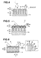
- FIG. 2 is a sectional view that illustrates the construction of the microstructure 2.
- the microstructure 2 is formed on a conductor 13, and is equipped with a dielectric base material 11 with a great number of regularly arranged fine holes 12, which are substantially the same shape in plan view, formed such that they are open at the surface 11s of the dielectric base material 11.
- a plurality of micro metal members 20, each of which have a filling portion 21 that fills one or more of the fine holes 12 and a protruding portion 22 that protrudes from the surface 11s of the base material 11 and is of a diameter, which is greater than the diameter of the filling portion, capable of inducing local plasmon, are fixed to the dielectric base material 11.
- the plurality of micro metal members 20 are those that have the same numbers of filling portions 21 that fill the same numbers of the fine holes 12.
- the micro metal members 20 of the microstructure 1 of the first embodiment had different numbers of filling portions 21 that fill different numbers of the fine holes 12.
- the microstructure 2 of the second embodiment differs in that the plurality of micro metal members 20 are those that have the same numbers of filling portions 21 that fill the same numbers of the fine holes 12. That is, there are fluctuations in the sizes of the protruding portions 22 in the first embodiment, whereas the sizes of the protruding portions 22 are substantially uniform in the microstructure 2 of the second embodiment.
- the microstructure 2 can be produced in the same manner as the microstructure 1 of the first embodiment, except that the micro metal members 20 are formed under conditions such that the number of fine holes 12 filled by the filling portions become equal.
- preferred materials for the microstructure 2 are the same as those for the microstructure 1 of the first embodiment.
- the micro metal members 20 each have a filling portion 21 that fills two or more fine holes12, and a protruding portion 22 that protrudes from the surface 11s of the base material 11 and is of a diameter, which is greater than the diameter of the filling portion 21, capable of inducing local plasmon.
- the filling portions 21 may be those that fill pluralities of the fine holes 12. Therefore, strict control of plating conditions is not necessary, compared to a structure in which a single protruding portion 22 corresponds to each filling portion 21 that fills the fine holes 12, which are microstructures on the order of nanometers.
- the microstructure 2 differs from the microstructure 1 of the first embodiment in that the sizes of the protruding portions 22 are substantially uniform. Therefore, the effects obtained due to the fluctuations of the sizes of the protruding portions 22 described in the first embodiment are not exhibited. However, because the structures are similar except for the point of uniformity in the sizes of the protruding portions 22, similar advantageous effects can be obtained.
- the wavelength at which local plasmon resonance is induced can be shifted to longer wavelengths, by increasing the number of fine holes 12 which are filled by the filling portions 21, thereby increasing the sizes of the protruding portions 22.
- the sizes of the protruding portions 22 vary according to plating conditions. Therefore, for example, in the case that electric field amplification effects are desired at longer wavelengths of incident light, the wavelength at which local plasmon resonance is induced can be shifted to longer wavelengths by a simple design choice of just changing the plating conditions.
- optical field amplifying devices 3 through 8 are equipped with the microstructure of the present invention. These embodiments will be described as being equipped with the microstructure 1, but the microstructure 2 may similarly be applied.
- the microstructure 1 generates an amplified electric field by the electric field amplification effect due to local plasmon resonance, when local plasmon resonance is induced by light irradiated onto the surface 1s thereof.
- the microstructure 1 can be applied favorably as an optical field amplifying device or as a base material for an optical field amplifying device.
- the optical field amplifying device of the present invention is equipped with the microstructure 1, and generates an amplified electric field on the surface 1s of the microstructure 1 when light is irradiated on the surface Is.
- optical field amplifying devices include: those that amplify the energy of light to be detected to improve detection sensitivity; those that perform sensing by utilizing changes of the optical properties of emitted light beams; and those that utilize the energy of incident light beams, which have been amplified by the electric filed amplifying effect.
- a Raman spectroscopy device 3 in which a sample is placed in contact with an electric field amplification region created by the local plasmon on the surface 1s of the microstructure 1; and Raman scattered light is generated by a measuring light beam L1 of a specific wavelength entering the sample, is an example of an optical field amplifying device that amplifies the energy of light to be detected to improve detection sensitivity.
- This type of Raman spectroscopy device may be employed in surface enhanced Raman detection, for detecting Raman scattered light, which is amplified by the electric field amplification effect, thereby improving detection sensitivity.
- a sensor device 4 in which a sample is placed in contact with an electric field amplification region created by the local plasmon on the surface 1s of the microstructure 1; and a measuring light beam L1 that enters the sample is emitted as emitted light beams having different physical properties, depending on the sample, is an example of an optical field amplifying device that performs sensing by utilizing changes of the optical properties of emitted light beams.
- a specific wavelength of a measuring light beam L1 is absorbed by the electric field amplification effect of local plasmon resonance induced thereby, and is emitted as a light beam having specific absorption properties.
- Sensing can be performed by detecting changes in the absorption properties, such as shifting in the peak absorbed wavelength, prior to and following contact of the sample.
- An ablation device 5 in which a target is placed in contact with an electric field amplification region created by the local plasmon on the surface 1s of the microstructure 1; an incident light beam L1 is irradiated onto the target; and the portion of the target irradiated by the laser beam is caused to transpire, is an example of an optical field amplifying device that utilizes the energy of incident light beams, which have been amplified by the electric filed amplifying effect.
- an optical field amplifying device that utilizes the energy of incident light beams which have been amplified by the electric filed amplifying effect is a mass spectroscopy device 6, in which a sample is placed in contact with an electric field amplification region created by local plasmon on the surface 1s of the microstructure 1; and a measuring light beam L1 is irradiated onto the sample, to desorb a target S of mass spectrometry, which is included in the sample, from the surface 1s.
- the energy of the incident light beam L1 which has been amplified by the electric field amplifying effect, is used to cause an irradiated portion of a target to transpire or to desorb the target S of mass spectroscopy. Therefore, the energy of the incident light beam L1 can be reduced.
- an optical field amplifying device that utilizes the energy of incident light beams which have been amplified by the electric filed amplifying effect is a light energy transfer element 7 (refer to Figure 5 ), in which photosystem complexes 30, constituted by energy donors 30D that absorb optical energy and donates energy, and energy acceptors 30A that receive the energy donated by the energy donors, are formed on the surfaces of the protruding portions 22 of the micro metal members 20; and wherein: an incident light beam L1 of a wavelength which is capable of inducing local plasmon at the protruding portions 22, and which includes a wavelength which enables absorption of optical energy by the energy donors 30D, is irradiated onto the surface 1s of the microstructure 1.
- the microstructure 1 can obtain electric field amplification effects at the protruding portions 22. Therefore, the energy of the incident light beam L1 is amplified at the protruding portions 22, the light absorption efficiency of the photosystem complexes 30 is increased, and light energy transfer efficiency (photoelectric conversion efficiency) can be obtained. Further, the micro metal members 20 on which the photosystem complexes 30 are formed are embedded within the dielectric base material 11. Therefore, the photosystem complexes 30 are stably held on the device, and the possibility that planar uniformity will decrease due to the photosystem complexes 30 flaking off is low. Light energy transfer elements are employed as artificial photosynthesis elements such as hydrogen generating elements, and as photovoltaic cells. The light energy transfer element 7 is capable of providing highly efficient artificial photosynthesis elements and photovoltaic cells.
- an optical field amplifying device that utilizes the energy of incident light beams which have been amplified by the electric filed amplifying effect is a sensor device 8 (refer to Figure 6 ), in which a sensing surface, to which only a specific target substance R bonds, is formed at an electric field amplification region created by the local plasmon on the surface 1s of the microstructure 1; and wherein: the specific target substance R is labeled with a fluorescent marker Lu; and a measuring light beam L1 of a wavelength which is capable of inducing local plasmon at the protruding portions 22, and of an absorption wavelength that causes two photon excited fluorescence emission or multiphoton excited fluorescence emission by the fluorescent marker Lu is irradiated onto the sensing surface, which is employed in sensing that detects the two photon excited fluorescence or the multiphoton excited fluorescence of the fluorescent marker Lu.
- the cross sectional absorption area of two photon excitation and multiphoton excitation is smaller than that of single photon excitation by an order of several powers of ten. Therefore, an expensive high energy light source had been necessary to obtain sufficient fluorescence emission.
- the microstructure 1 can obtain an effective electric field amplification effect at the protruding portions 22. Therefore, remarkable improvements in transition probability can be obtained by the energy of the measuring light beam L1, which is amplified by the electric field amplification effect. Accordingly, the light source can be a low energy light source.
- the micro metal members 20 are formed by administering plating to the interiors of the fine holes 12.
- the method by which the micro metal members 20 are produced and the method by which the fine holes 12 are filled are not limited to a plating process.
- the conductor 13 is the non anodized portion of the metal material 10.
- the conductor 13 may be constituted by metal which is provided on the bottom surface 11b of the dielectric base material 11 by vapor deposition or the like.
- the material for the conductor 13 is not limited, and conductive materials, such as metals and ITO (Indium Tin Oxide) may be employed.
- the dielectric base material 11 may have fine apertures 12 that penetrate therethrough formed therein.
- the method by which the fine apertures 12 are formed is not limited. Examples include: completely anodizing the metal material 10; and partially anodizing the metal material 10, then removing portions of the dielectric base material 11 from the side of the bottom surface 11b thereof.
- the conductor 13 may be removed after the micro metal members 20 are formed.
- A1 was described as being the main component of the metal material 10 which is employed to produce the dielectric base material 11.
- any desired metal may be used, as long as anodization thereof is possible.
- examples of such metals include; Ti, Ta, Hf, Zr, Si, In, and Zn.
- the metal material 10 may include two or more types of anodizable metals.
- the pattern of the fine holes 12 in plan view changes according to the type of metal material 10 which is used. However, The dielectric base material 11 will still have fine holes 12 which are of substantially the same shape in plan view, and which are arranged adjacent to each other.
- anodization is utilized to arrange the fine holes 12 in a regular manner.
- the method by which the fine holes 12 are formed is not limited to anodization. Anodization is preferable because it is capable of handing large areas and does not require costly equipment.
- Other examples of microprocessing methods by which the fine holes 12 may be formed include: forming a plurality of regularly arranged recesses in the surface of a resin substrate by a nano imprinting method; and forming a plurality of regularly arranged recesses in the surface of a metal substrate by an electron lithography technique that uses a focused ion beam (FIB), an electron beam (EB) or the like.
- FIB focused ion beam
- EB electron beam
- the sizes and arrangement of the fine holes 12 within the dielectric base material 11 are substantially regular, because adjustments to conditions during formation of the micro metal members 20 is facilitated in this case. However, it is not necessary for the sizes and arrangement of the fine holes 12 to be substantially regular.
- the microstructure 1 of the first embodiment was produced by the following steps.
- An aluminum plate (99.99% pure A1, at a thickness of 10nm) was prepared as the metal material 10 to be anodized.
- the aluminum plate was used as an anode, and aluminum was used as a cathode, and anodization was performed under conditions that would result in a portion of the aluminum plate becoming an alumina layer 30. Thereby, the dielectric base material 11 and the conductor 13, which is a portion of the metal material 10 that was not anodized, were obtained.
- Anodization was performed according to the two step anodizing process disclosed in H. Masuda and M. Sato, "Fabrication of Gold Nanodot Array Using Anodic Porous Alumina as an Evaporation Mask", J. J. Appl. Phys. Vol. 35, pp. L126-L129 (1996 ). The anodizing conditions were the same as those described in this document.
- the great number of fine holes 12 within the dielectric base material 11 were filled with Au by plating, using the conductor 13 as an electrode, to form the micro metal members 20.
- a microstructure (Raman spectroscopy device) was obtained.
- the plating process was conducted using a 40mM tetrachloroauric acid solution, with an applied voltage of 12V at one second cycles with a duty ratio of 0.1 for 10 minutes.
- Au was deposited on glass subtrates by vacuum vapor deposition, to form island structured films, which are said to have surface enhancing Raman effects.
- vapor deposition was performed under conditions such that the entire surface of the glass substrate is covered by Au, and such that the thickness of the film is 10nm, to form a comparative Raman spectroscopy device.
- an annealing process was administered on the glass substrate having the 10nm thick island structured film on the surface thereof at a temperature of 50°C for five minutes, to form another comparative Raman spectroscopy device.
- a laser having an oscillation wavelength of 785nm was used as a light source, and measurements were performed with equal laser power for all three examples.
- a 150L/mm spectroscopic detector was used as a spectroscopic means.
- the sample fluid was a rhodamine 6G (R6G) solution which was diluted to several mM. R6G is known to have a Raman spectral peak at 1360cm -1 .
- the Raman spectrum obtained by each example is illustrated in Figures 8A through 8C , respectively.
- the vertical axes of the graphs represent intensity at 500 (a.u.) per tick mark.
- the Raman spectroscopy device of Example 1 has stronger amplified signals within the range of 500cm -1 to 1700cm -1 over the comparative examples 1 and 2, thereby proving the effectiveness of the present invention.
- the microstructure of the present invention can be favorably utilized as a sensor device used in biosensors, a Raman spectroscopy device, a mass spectrometry device, an ablation substrate, and as a light energy transfer element.
Landscapes
- Health & Medical Sciences (AREA)
- Chemical & Material Sciences (AREA)
- Immunology (AREA)
- Physics & Mathematics (AREA)
- General Physics & Mathematics (AREA)
- Analytical Chemistry (AREA)
- Biochemistry (AREA)
- General Health & Medical Sciences (AREA)
- Life Sciences & Earth Sciences (AREA)
- Pathology (AREA)
- Nuclear Medicine, Radiotherapy & Molecular Imaging (AREA)
- Engineering & Computer Science (AREA)
- Nanotechnology (AREA)
- Chemical Kinetics & Catalysis (AREA)
- Optics & Photonics (AREA)
- Investigating, Analyzing Materials By Fluorescence Or Luminescence (AREA)
- Optical Integrated Circuits (AREA)
Abstract
Description
- The present invention relates to a microstructure equipped with a dielectric base material having a plurality of fine holes in the surface thereof and metal members capable of inducing local plasmon, a method for producing the microstructure, and an optical field amplifying device that utilizes the microstructure.
- Light energy transfer elements that efficiently utilize solar energy, are being considered. Solar energy is being investigated as a new, clean, and safe alternative energy source to replace fossil fuels such as oil. The photosynthesis function of plants has been noted as a highly efficient method of light energy transfer, and there is expectation for development of artificial light energy transfer elements (artificial photosynthesis elements) equipped with artificially constructed photosystem complexes that have photosynthesis functions.
- Japanese Unexamined Patent Publication Nos.
2001-303022 2002-25635 - In order to obtain higher efficiency, light energy transfer elements that employ microstructures having electric field amplifying effects on the surfaces thereof as the base material on which the photosystem complexes are provided are being considered. Japanese Unexamined Patent Publication No.
2005-259674 - Japanese Unexamined Patent Publication No.
2004-530867 U.S. Patent No. 7,288,419 discloses a microstructure equipped with a dielectric base material and a plurality of fine metal particles. In this microstructure, highly densely arranged fine holes are provided in the surface of the dielectric base material, and each of the metal particles includes a filling portion that fills a fine hole, and a head portion that protrudes from the surface of the dielectric base material and which are of a size capable of inducing local plasmon resonance. - However, in the microstructures disclosed by Japanese Unexamined Patent Publication Nos.
2005-259674 2004-530867 - In the microstructure disclosed by
U.S. Patent No. 7,288,419 , the metal particles which are capable of inducing local plasmon are embedded in the base material. Therefore, the metal particles are less likely to flake off than in the structures disclosed by Japanese Unexamined Patent Publication Nos.2005-259674 2004-530867 - However, it is necessary to form the metal particles such that a single head portion corresponds to each filling portion that fills the fine holes, which are arranged at high density within the surface of the dielectric base material. The process for forming a head portion for each of the plurality of filling portions, which are microstructures on the order of nanometers, is not easy, and there is a possibility that yield will suffer.
- The present invention has been developed in view of the foregoing circumstances. It is an object of the present invention to provide a microstructure that exhibits electric field amplification effects having high planar uniformity and which can be produced by a simple process. The microstructure may be employed as an optical field amplifying device, for a light energy transfer element or the like. It is another object of the present invention to provide a method for manufacturing the microstructure.
- It is still another object of the present invention to provide an optical field amplifying device which is equipped with the aforementioned microstructure.
- A first microstructure of the present invention comprises:
- a dielectric base material having a great number of fine holes which are open at the surface of the base material; and
- a plurality of micro metal members, each of which have a filling portion that fills one or more of the fine holes and a protruding portion that protrudes from the surface of the base material and is of a diameter greater than the diameter of the filling portion, capable of inducing local plasmon; and is characterized by:
- the plurality of micro metal members including those that have different numbers of filling portions that fill different numbers of the fine holes.
- In the present specification the term "great number" is defined as a number far greater than the number of fine holes which are filled by the filling portions.
- In addition, the "diameter" of the protruding portion is defined as the maximum diameter thereof.
- A second microstructure of the present invention comprises:
- a dielectric base material having a great number of fine holes which are open at the surface of the base material; and
- a plurality of micro metal members, each of which have a filling portion that fills one or more of the fine holes and a protruding portion that protrudes from the surface of the base material and is of a diameter greater than the diameter of the filling portion, capable of inducing local plasmon; and is characterized by:
- the plurality of micro metal members being those that have the same numbers of filling portions that fill the fine holes.
- It is preferable for the average distance between adjacent protruding portions to be 10nm or less. Here, the term "distance" refers to the distance between the closest portions of separate and adjacent protruding portions.
- It is preferable for the distribution of the fine holes within the dielectric base material to be substantially regular.
- It is preferable for the dielectric base material to be formed by a metal oxide which is obtained by anodizing at least a portion of a metallic material, and for the fine holes to be formed within the metal oxide during the anodizing process.
- The micro metal members may be formed by plating the interiors of the fine holes formed in the dielectric base material until a portion of the plating protrudes from the surface of the dielectric base material.
- An optical field amplifying device of the present invention is equipped with the microstructure of the present invention, and is characterized by:
- an amplified electric field being generated on the surface of the microstructure due to the electric field amplifying effect of local plasmon, which is induced by light being irradiated on said surface.
- A preferred example of the optical field amplifying device of the present invention has a sample placed in contact with an electric field amplification region created by the local plasmon on the surface thereof; and a measuring light beam that enters the sample is emitted as emitted light beams having different physical properties, depending on the sample.
- Another preferred example of the optical field amplifying device of the present invention has a sample placed in contact with an electric field amplification region created by the local plasmon on the surface of the optical amplifying device; and Raman scattered light is generated by a measuring light beam of a specific wavelength entering the sample.
- Still another preferred example of the optical field amplifying device of the present invention has a target placed in contact with an electric field amplification region created by the local plasmon on the surface of the optical amplifying device; a laser beam is irradiated onto the target; and the portion of the target irradiated by the laser beam is caused to transpire.
- Still yet another preferred example of the optical field amplifying device of the present invention has a sample placed in contact with an electric field amplification region created by the local plasmon on the surface of the optical amplifying device; and a measuring light beam is irradiated onto the sample, to desorb a target of mass spectrometry, which is included in the sample, from the surface.
- The optical field amplifying device of the present invention may further comprise:
- photosystem complexes, constituted by energy donors that absorb optical energy and donates energy, and energy acceptors that receive the energy donated by the energy donors, formed on the surfaces of the protruding portions of the micro metal members; and be characterized by:
- an incident light beam of a wavelength which is capable of inducing local plasmon at the protruding portions, and which includes a wavelength which enables absorption of optical energy by the energy donors, being irradiated onto the surface of the optical field amplifying device.
- The optical field amplifying device of the present invention may further comprise:
- a sensing surface, to which only a specific target substance bonds, formed at an electric field amplification region created by the local plasmon on the surface of the optical field amplifying device; and be characterized by:
- the specific target substance being labeled with a fluorescent marker that selectively bonds with the target substance;
- a measuring light beam of a wavelength which is capable of inducing local plasmon at the protruding portions, and of an absorption wavelength that causes two photon excited fluorescence emission or multiphoton excited fluorescence emission by the fluorescent marker being irradiated onto the sensing surface; and
- the optical field amplifying device being employed in sensing that detects the two photon excited fluorescence or the multiphoton excited fluorescence of the fluorescent marker.
- A method for producing a microstructure capable of inducing local plasmon on the surface thereof of the present invention comprises the steps of:
- preparing a dielectric base material having a great number of fine holes which are open on the surface thereof; and
- plating the interiors of the fine holes formed in the dielectric base material such that metal fills the interiors of the fine holes; and
- continuing plating until the metal protrudes from the surface of the dielectric base material at diameters greater than those of the fine holes.
- In the microstructure of the present invention, each of the plurality of micro metal members have a filling portion that fills one or more of the fine holes and a protruding portion that protrudes from the surface of the base material. Each of the protruding
portions 22 is of a diameter, which is greater than the diameter of the filling portion and capable of inducing local plasmon. Therefore, the head portions can be provided close to each other, and effective electric field amplification functions can be obtained. - In addition, the micro metal members are of structures wherein portions thereof are embedded in the fine holes of the dielectric base material. Therefore, the micro metal members are not likely to flake off from the dielectric base material, and an electric field amplification effect having high planar uniformity is exhibited. Further, the micro metal members include those of which the filling portions fill a plurality of the fine holes. Accordingly, strict control of the production process is obviated, that is, the micro metal members can be produced by a simple process.
- In the first microstructure of the present invention, the micro metal members include those that have different numbers of filling portions that fill different numbers of the fine holes. In this case, the sizes of the protruding portions become non uniform. The wavelength at which an electric field amplifying effect due to local plasmon can be obtained varies according to the type of metal and the size thereof. Therefore, the first microstructure of the present invention, in which the sizes of the protruding portions are not uniform, the wavelengths at which the electric field amplification effect can be obtained are broadened, corresponding to the fluctuation in the sizes of the protruding portions.
-
-
Figure 1 is a sectional view that illustrates the construction of a microstructure according to a first embodiment of the present invention, taken along the thickness direction thereof. -
Figure 2A, Figure 2B, Figure 2C, and Figure 2D are perspective views that illustrate the manufacturing steps of the microstructure according to the first embodiment. -
Figure 3A, Figure 3B, Figure 3C, and Figure 3D are sectional views corresponding toFigure 2A, Figure 2B, Figure 2C, and Figure 2D , respectively. -
Figure 4 is a sectional view that illustrates the construction of a microstructure according to a second embodiment of the present invention, taken along the thickness direction thereof. -
Figure 5 is a sectional view that illustrates the construction of a light energy transfer element, which is a preferred embodiment of the optical field amplifying device of the present invention, taken along the thickness direction thereof. -
Figure 6 is a sectional view that illustrates the construction of a two photon fluorescence excitation sensor, which is a preferred embodiment of the optical field amplifying device of the present invention, taken along the thickness direction thereof. -
Figure 7A is a sectional SEM photograph of the microstructure (Raman spectroscopy device) of the first embodiment taken along the thickness direction thereof. -
Figure 7B is an SEM photograph of the surface of the microstructure of the first embodiment. -
Figure 8A is a graph that illustrates the Raman spectrum of a first comparative example,Figure 8B is a graph that illustrates the Raman spectrum of a second comparative example, andFigure 8C is a graph that illustrates the Raman spectrum of an Example of the present invention. - A
microstructure 1 according to a first embodiment of the present invention will be described with reference to the drawings.Figure 1 is a sectional view that illustrates the construction of themicrostructure 1.Figure 2 andFigure 3 are diagrams that illustrate the manufacturing steps of the microstructure according to the first embodiment, whereinFigure 2 shows perspective views of each step, andFigure 3 shows sectional views of each step. - As illustrated in
Figure 1 , themicrostructure 1 is formed on aconductor 13, and is equipped with adielectric base material 11 with a great number of regularly arrangedfine holes 12, which are substantially the same shape in plan view, formed such that they are open at thesurface 11s of thedielectric base material 11. A plurality ofmicro metal members 20, each of which have a fillingportion 21 that fills one or more of the fine holes 12 and a protrudingportion 22 that protrudes from thesurface 11s of thebase material 11 and is of a diameter, which is greater than the diameter of the filling portion, capable of inducing local plasmon, are fixed to thedielectric base material 11. The plurality ofmicro metal members 20 include those that have different numbers of fillingportions 21 that fill different numbers of the fine holes 12. - An incident light beam L1 that includes wavelengths of light capable of inducing local plasmon at the protruding
portions 22 is irradiated onto thesurface 11s of thedielectric base material 11 of themicrostructure 1. The incident light beam L1 is not particularly limited, and may be natural light, such as sunlight, a light beam emitted by a specific light source, or a broad wavelength band light beam. The incident light beam L1 causes Local plasmon to be induced at the protrudingportions 22 of themicrostructure 1, and an electric field amplifying effect is obtained due to the local plasmon. The electric field amplification effect due to local plasmon is said to be a hundredfold or greater at the local plasmon resonance wavelength. Accordingly, it is preferable for the incident light beam L1 to include a wavelength of light that causes local plasmon resonance at the protrudingportions 22, in order to obtain greater electric field amplification effects. - The fine holes 12 extend substantially straight in the thickness direction of the
microstructure 1 from thesurface 11s of thedielectric base material 11. The fine holes 12 are closed at thebottom surface 11b of thedielectric base material 11, and do not penetrate therethrough. - In the first embodiment, the
dielectric base material 11 is an alumina (Al2O3) layer 11 (metal oxide layer) which is obtained by partially anodizing ametal material 10 having aluminum (Al) as its main component and which may have slight impurities contained therein, as illustrated inFigure 2 andFigure 3 . As illustrated inFigure 2 andFigure 3 , the fine holes 12 are formed as holes having rounded bottoms during the partial anodizing process. The remaining non anodized portion of themetal material 10 becomes theconductor 13. - The shape of the
metal material 10 to be anodized is not limited. A metal plate is an example. In addition, themetal material 10 may be formed as a layer on a substrate. - Anodization may be executed by using the
metal material 10 as an anode, using carbon, aluminum, or the like as a cathode (opposing electrode), soaking the anode and the cathode in an anodizing electrolytic solution, then applying voltage therebetween. The electrolytic solution is not particularly limited. Acidic electrolytic solutions that include at least one of: sulfuric acid; phosphoric acid; chromic acid; oxalic acid; sulfamic acid; benzene sulfonic acid; amide sulfonic acid; and the like may be favorably employed. - By anodizing the
metal material 10 illustrated inFigure 2A andFigure 3A , an oxidation reaction progresses substantially in the vertical direction from thesurface 10s thereof (the upper surface in the Figures) as illustrated inFigure 2B andFigure 3B , to form thealumina layer 11. - The
alumina layer 11 formed by anodization is of a structure in whichfine columns 14 which are substantially hexagonal in plan view are arranged adjacent to each other. The fine holes 12 that extend in the depth direction from thesurface 10s are formed at the approximate centers of each of thefine columns 14. The bottom surfaces of the fine holes 12 and thefine columns 14 are rounded in shape, as illustrated inFigure 2 andFigure 3 . The structure of alumina layers which are formed by anodization is described in H. Masuda, "Preparation of Mesoporous Alumina and Applications as a Functional Material", Material Science, pp. 34, Vol. 15, No. 10, 1997. - In the first embodiment, partial anodization is performed on the
metal material 10. In the case that oxalic acid is employed as the electrolytic solution, an example of favorable anodization conditions are: an electrolytic solution concentration of 0.5M; a solution temperature of 15°C; and an applied voltage of 40V. By performing anodization under these conditions, the alumina layer 11 (dielectric base material), in which the great number offine holes 12 of substantially the same shape in plan view and which are open at thesurface 11s of the dielectric base material are formed, can be obtained. - Generally, the pitch among adjacent fine holes 12 can be controlled to be within a range of 10nm to 500nm. The diameters of the fine holes 12 can be controlled to be within a range of 5nm to 400nm. Japanese Unexamined Patent Publication Nos.
2001-9800 2001-138300 - The
micro metal members 20, which are constituted by the fillingportions 21 and the protrudingportions 22, are formed by administering electroplating within the fine holes 12 of thedielectric base material 11, as illustrated inFigure 2C andFigure 3C . In this case, the anodizedalumina layer 11 is present between theconductor 13 and the bottoms of the fine holes 12. However, by forming thealumina layer 11 at the bottoms of the fine holes 12 sufficiently thin such that conduction is enabled between theconductor 13 and the solution that contains metal within the fine holes 12, electroplating using theconductor 13 as an electrode enables prioritized separation of the metal from the bottoms of the fine holes 12, where electric fields are powerful. - Electroplating using the
conductor 13 as an electrode enables prioritized separation of the metal from the bottoms of the fine holes 12, where electric fields are powerful. Therefore, by continuously performing electroplating, the metal fills the interiors of the fine holes 12, to form the fillingportions 21 of themicro metal members 20. When electroplating is continued after the fillingportions 21 are formed, the metal overflows from the fine holes 12. However, because electric fields are powerful in the vicinities of the fine holes 12, the metal that overflows is isotropically plated at the peripheries of the fine holes 12. The metal which is plated at the peripheries of the fine holes 12 protrude from thesurface 11s of thedielectric base material 11 above the fillingportions 21, and become the protrudingportions 22 which have diameters greater than those of the filling portions 21 (refer toFigure 2D andFigure 3D ). - The
microstructure 1 is equipped withmicro metal members 20 having fillingportions 21 that fill different numbers of the fine holes 12. The sizes of the protrudingportions 22 of themicro metal members 20 change according to the number offine holes 12 which are filled by the fillingportions 21 thereof. For example, in the case that the fine holes 12 which have substantially uniform diameters are arranged substantially regularly, if the number offine holes 12 filled by the fillingportion 21 is doubled, the size of the protrudingportion 22 is approximately doubled. - It is necessary to strictly control the plating conditions in order to form the
micro metal members 20 such that each fillingportion 21 that fills a singlefine hole 12 has a single protrudingportion 22. Themicrostructure 1 of the first embodiment is equipped withmicro metal members 20 having fillingportions 21 that fill different numbers of the fine holes 12. Therefore, it is not necessary to strictly control the plating conditions. Accordingly, themicrostructure 1 can be produced by a simple process. - The wavelength at which local plasmon resonance wavelength occurs varies according to the type of metal and the size thereof. Accordingly, if there are fluctuations in the number of
fine holes 12 which are filled by thefiling portions 21, the sizes of the protrudingportions 22 that induce local plasmon also fluctuate. As a result, the wavelengths at which local plasmon can be induced are broadened, corresponding to the fluctuation in the sizes of the protrudingportions 22. - In addition, the number of
fine holes 12 which are filled by the fillingportions 21 can be adjusted by the plating conditions when forming the protrudingportions 22. Therefore, the wavelength or the wavelength range at which local plasmon is induced can be varied by changing the plating conditions. If plating is continued after a protrudingportion 22 is formed on a fillingportion 21 that fills a singlefine hole 12, adjacent protrudingportions 22 contact each other and become integrated. As a result, single protrudingportions 22 which are formed by two protrudingportions 22 andmicro metal members 22 which are formed by two fillingportions 21 that fill twofine holes 12 can be formed. The sizes of the protrudingportions 22 can be varied by adjusting the number of protrudingportions 22 to be integrated, by the simple process of merely changing the plating conditions. - If the size of the protruding
portions 22 is large enough to induce local plasmon, there is no limitation on the number offine holes 12 which are filled by the fillingportions 21. From the viewpoint of broadening the wavelength band at which local plasmon resonance can be induced, it is preferable for themicrostructure 1 to includemicro metal members 20 having fillingportions 21 that fill single fine holes 12. Taking the wavelength and the like of the incident light beam L1 into consideration, it is preferable for the sizes of the protrudingportions 22 to be within a range of 10nm to 300nm. Protrudingportions 22 of sizes within this range are capable of inducing local plasmon with light beams within a wavelength range from 300nm to near infrared. - It is preferable for adjacent protruding
portions 22 to be separated. It is preferable for the average value of distances w among adjacent protrudingportions 22 to be within a range of several nm to 10nm. Electric field amplification effects are known to be particularly powerful when the distance w is 10nm or less. Accordingly, if the average value of the distances w is within the aforementioned range, an electric field amplification effect due to local plasmon can be effectively obtained. - Local plasmon resonance is a phenomenon in which free electrons within metals resonate with the electric field of light and vibrate, thereby generating strong electric fields in the vicinity of the metals. Therefore, the
micro metal members 20 may be any metal that has free electrons. Themicrostructure 1 induces local plasmon at the protrudingportions 22 when the incident light beam L1 is irradiated onto thesurface 11s of the dielectric base material. Therefore, metals that generate local plasmon are preferred as materials for themicro metal members 20. Examples of such materials are Au, Ag, Cu, Pt, Ni, and Ti. Au and Ag, which have high electric field amplification effects, are particularly preferable. - Being of the construction described above, the microstructure illustrated in
Figure 2D andFigure 3D are capable of effectively generating electrical field amplification effects due to local plasmon at the protrudingportions 22. - In the
microstructure 1, each of themicro metal members 20 have a fillingportion 21 that fills one or more of the fine holes 12 and a protrudingportion 22 that protrudes from thesurface 11s of thedielectric base material 11. Each of the protrudingportions 22 is of a diameter, which is greater than the diameter of the fillingportions 21 and capable of inducing local plasmon. Therefore, the head portions can be provided close to each other, and effective electric field amplification functions can be obtained. - In addition, the
micro metal members 20 are of structures wherein portions thereof are embedded in the fine holes 12 of thedielectric base material 11. Therefore, themicro metal members 20 are not likely to flake off from thedielectric base material 11, and an electric field amplification effect having high planar uniformity is exhibited. Further, themicro metal members 20 include those of which the fillingportions 21 fill a plurality of the fine holes 12. Accordingly, strict control of the production process is obviated, that is, themicro metal members 20 can be produced by a simple process. - In the
microstructure 1, themicro metal members 20 include those that have different numbers of fillingportions 21 that fill different numbers of the fine holes 12. In this case, the sizes of the protrudingportions 22 become non uniform. The wavelength at which an electric field amplifying effect due to local plasmon can be obtained varies according to the type of metal and the size thereof. Therefore, themicrostructure 1, in which the sizes of the protrudingportions 22 are not uniform, the wavelengths at which the electric field amplification effect can be obtained are broadened, corresponding to the fluctuation in the sizes of the protrudingportions 22. - A
microstructure 2 according to a second embodiment of the present invention will be described with reference to the drawings.Figure 4 is a sectional view that illustrates the construction of themicrostructure 2. - As illustrated in
Figure 4 , themicrostructure 2 is formed on aconductor 13, and is equipped with adielectric base material 11 with a great number of regularly arrangedfine holes 12, which are substantially the same shape in plan view, formed such that they are open at thesurface 11s of thedielectric base material 11. A plurality ofmicro metal members 20, each of which have a fillingportion 21 that fills one or more of the fine holes 12 and a protrudingportion 22 that protrudes from thesurface 11s of thebase material 11 and is of a diameter, which is greater than the diameter of the filling portion, capable of inducing local plasmon, are fixed to thedielectric base material 11. In the second embodiment, the plurality ofmicro metal members 20 are those that have the same numbers of fillingportions 21 that fill the same numbers of the fine holes 12. - The
micro metal members 20 of themicrostructure 1 of the first embodiment had different numbers of fillingportions 21 that fill different numbers of the fine holes 12. In contrast, themicrostructure 2 of the second embodiment differs in that the plurality ofmicro metal members 20 are those that have the same numbers of fillingportions 21 that fill the same numbers of the fine holes 12. That is, there are fluctuations in the sizes of the protrudingportions 22 in the first embodiment, whereas the sizes of the protrudingportions 22 are substantially uniform in themicrostructure 2 of the second embodiment. - Accordingly, the
microstructure 2 can be produced in the same manner as themicrostructure 1 of the first embodiment, except that themicro metal members 20 are formed under conditions such that the number offine holes 12 filled by the filling portions become equal. In addition, preferred materials for themicrostructure 2 are the same as those for themicrostructure 1 of the first embodiment. - In the
microstructure 2, themicro metal members 20 each have a fillingportion 21 that fills two or more fine holes12, and a protrudingportion 22 that protrudes from thesurface 11s of thebase material 11 and is of a diameter, which is greater than the diameter of the fillingportion 21, capable of inducing local plasmon. - In this structure, the filling
portions 21 may be those that fill pluralities of the fine holes 12. Therefore, strict control of plating conditions is not necessary, compared to a structure in which asingle protruding portion 22 corresponds to each fillingportion 21 that fills the fine holes 12, which are microstructures on the order of nanometers. - As described above, the
microstructure 2 differs from themicrostructure 1 of the first embodiment in that the sizes of the protrudingportions 22 are substantially uniform. Therefore, the effects obtained due to the fluctuations of the sizes of the protrudingportions 22 described in the first embodiment are not exhibited. However, because the structures are similar except for the point of uniformity in the sizes of the protrudingportions 22, similar advantageous effects can be obtained. - In the second embodiment, the wavelength at which local plasmon resonance is induced can be shifted to longer wavelengths, by increasing the number of
fine holes 12 which are filled by the fillingportions 21, thereby increasing the sizes of the protrudingportions 22. The sizes of the protrudingportions 22 vary according to plating conditions. Therefore, for example, in the case that electric field amplification effects are desired at longer wavelengths of incident light, the wavelength at which local plasmon resonance is induced can be shifted to longer wavelengths by a simple design choice of just changing the plating conditions. - The construction of optical field amplifying devices according to embodiments of the present invention will be described with reference to the drawings. As illustrated in
Figure 1 andFigures 4 through6 , optical field amplifying devices 3 through 8 are equipped with the microstructure of the present invention. These embodiments will be described as being equipped with themicrostructure 1, but themicrostructure 2 may similarly be applied. - Local plasmon resonance occurs at the surfaces of the protruding
portions 22 of the micro metal members at thesurface 1s of themicrostructure 1. The drawings are magnified to facilitate visual representations, and therefore the protrusions and recesses formed by the protrudingportions 22 appear to be prominent. However, because the actual dimensions are on the order of nanometers, the protrusions and recesses are small, and the plurality of protrudingportions 22 constitute thesurface 1s of themicrostructure 1. Accordingly, themicrostructure 1 generates an amplified electric field by the electric field amplification effect due to local plasmon resonance, when local plasmon resonance is induced by light irradiated onto thesurface 1s thereof. Themicrostructure 1 can be applied favorably as an optical field amplifying device or as a base material for an optical field amplifying device. - The optical field amplifying device of the present invention is equipped with the
microstructure 1, and generates an amplified electric field on thesurface 1s of themicrostructure 1 when light is irradiated on the surface Is. Examples of optical field amplifying devices include: those that amplify the energy of light to be detected to improve detection sensitivity; those that perform sensing by utilizing changes of the optical properties of emitted light beams; and those that utilize the energy of incident light beams, which have been amplified by the electric filed amplifying effect. - A Raman spectroscopy device 3, in which a sample is placed in contact with an electric field amplification region created by the local plasmon on the
surface 1s of themicrostructure 1; and Raman scattered light is generated by a measuring light beam L1 of a specific wavelength entering the sample, is an example of an optical field amplifying device that amplifies the energy of light to be detected to improve detection sensitivity. This type of Raman spectroscopy device may be employed in surface enhanced Raman detection, for detecting Raman scattered light, which is amplified by the electric field amplification effect, thereby improving detection sensitivity. - A sensor device 4, in which a sample is placed in contact with an electric field amplification region created by the local plasmon on the
surface 1s of themicrostructure 1; and a measuring light beam L1 that enters the sample is emitted as emitted light beams having different physical properties, depending on the sample, is an example of an optical field amplifying device that performs sensing by utilizing changes of the optical properties of emitted light beams. For example, in the case of a local plasmon sensor, a specific wavelength of a measuring light beam L1 is absorbed by the electric field amplification effect of local plasmon resonance induced thereby, and is emitted as a light beam having specific absorption properties. Sensing can be performed by detecting changes in the absorption properties, such as shifting in the peak absorbed wavelength, prior to and following contact of the sample. - An ablation device 5, in which a target is placed in contact with an electric field amplification region created by the local plasmon on the
surface 1s of themicrostructure 1; an incident light beam L1 is irradiated onto the target; and the portion of the target irradiated by the laser beam is caused to transpire, is an example of an optical field amplifying device that utilizes the energy of incident light beams, which have been amplified by the electric filed amplifying effect. Another example of an optical field amplifying device that utilizes the energy of incident light beams which have been amplified by the electric filed amplifying effect is a mass spectroscopy device 6, in which a sample is placed in contact with an electric field amplification region created by local plasmon on thesurface 1s of themicrostructure 1; and a measuring light beam L1 is irradiated onto the sample, to desorb a target S of mass spectrometry, which is included in the sample, from thesurface 1s. In these devices, the energy of the incident light beam L1, which has been amplified by the electric field amplifying effect, is used to cause an irradiated portion of a target to transpire or to desorb the target S of mass spectroscopy. Therefore, the energy of the incident light beam L1 can be reduced. - Another example of an optical field amplifying device that utilizes the energy of incident light beams which have been amplified by the electric filed amplifying effect is a light energy transfer element 7 (refer to
Figure 5 ), in which photosystemcomplexes 30, constituted byenergy donors 30D that absorb optical energy and donates energy, andenergy acceptors 30A that receive the energy donated by the energy donors, are formed on the surfaces of the protrudingportions 22 of themicro metal members 20; and wherein: an incident light beam L1 of a wavelength which is capable of inducing local plasmon at the protrudingportions 22, and which includes a wavelength which enables absorption of optical energy by theenergy donors 30D, is irradiated onto thesurface 1s of themicrostructure 1. Themicrostructure 1 can obtain electric field amplification effects at the protrudingportions 22. Therefore, the energy of the incident light beam L1 is amplified at the protrudingportions 22, the light absorption efficiency of thephotosystem complexes 30 is increased, and light energy transfer efficiency (photoelectric conversion efficiency) can be obtained. Further, themicro metal members 20 on which thephotosystem complexes 30 are formed are embedded within thedielectric base material 11. Therefore, thephotosystem complexes 30 are stably held on the device, and the possibility that planar uniformity will decrease due to thephotosystem complexes 30 flaking off is low. Light energy transfer elements are employed as artificial photosynthesis elements such as hydrogen generating elements, and as photovoltaic cells. The lightenergy transfer element 7 is capable of providing highly efficient artificial photosynthesis elements and photovoltaic cells. - Still another example of an optical field amplifying device that utilizes the energy of incident light beams which have been amplified by the electric filed amplifying effect is a sensor device 8 (refer to
Figure 6 ), in which a sensing surface, to which only a specific target substance R bonds, is formed at an electric field amplification region created by the local plasmon on thesurface 1s of themicrostructure 1; and wherein: the specific target substance R is labeled with a fluorescent marker Lu; and a measuring light beam L1 of a wavelength which is capable of inducing local plasmon at the protrudingportions 22, and of an absorption wavelength that causes two photon excited fluorescence emission or multiphoton excited fluorescence emission by the fluorescent marker Lu is irradiated onto the sensing surface, which is employed in sensing that detects the two photon excited fluorescence or the multiphoton excited fluorescence of the fluorescent marker Lu. - The cross sectional absorption area of two photon excitation and multiphoton excitation is smaller than that of single photon excitation by an order of several powers of ten. Therefore, an expensive high energy light source had been necessary to obtain sufficient fluorescence emission. However, the
microstructure 1 can obtain an effective electric field amplification effect at the protrudingportions 22. Therefore, remarkable improvements in transition probability can be obtained by the energy of the measuring light beam L1, which is amplified by the electric field amplification effect. Accordingly, the light source can be a low energy light source. - In the above embodiments, the
micro metal members 20 are formed by administering plating to the interiors of the fine holes 12. However, the method by which themicro metal members 20 are produced and the method by which the fine holes 12 are filled are not limited to a plating process. - In the above embodiments, the
conductor 13 is the non anodized portion of themetal material 10. However, theconductor 13 may be constituted by metal which is provided on thebottom surface 11b of thedielectric base material 11 by vapor deposition or the like. In this case, the material for theconductor 13 is not limited, and conductive materials, such as metals and ITO (Indium Tin Oxide) may be employed. - The above embodiments have been described as cases in which the fine holes 12 do not penetrate through the
dielectric base material 11. Alternatively, thedielectric base material 11 may havefine apertures 12 that penetrate therethrough formed therein. The method by which thefine apertures 12 are formed is not limited. Examples include: completely anodizing themetal material 10; and partially anodizing themetal material 10, then removing portions of thedielectric base material 11 from the side of thebottom surface 11b thereof. - The above embodiments have been described as cases in which the
conductor 13 is provided on thebottom surface 11b of thedielectric base material 11. However, in the case that conductivity of the fine holes 12 is not required, unlike the case in which electroplating is performed to fill the fine holes 12 with the fillingportions 21 of themicro metal members 20, theconductor 13 is not necessary. - Alternatively, the
conductor 13 may be removed after themicro metal members 20 are formed. - In the above embodiments, A1 was described as being the main component of the
metal material 10 which is employed to produce thedielectric base material 11. However, any desired metal may be used, as long as anodization thereof is possible. Examples of such metals include; Ti, Ta, Hf, Zr, Si, In, and Zn. Themetal material 10 may include two or more types of anodizable metals. - The pattern of the fine holes 12 in plan view changes according to the type of
metal material 10 which is used. However, Thedielectric base material 11 will still havefine holes 12 which are of substantially the same shape in plan view, and which are arranged adjacent to each other. - Cases have been described in which anodization is utilized to arrange the fine holes 12 in a regular manner. However, the method by which the fine holes 12 are formed is not limited to anodization. Anodization is preferable because it is capable of handing large areas and does not require costly equipment. Other examples of microprocessing methods by which the fine holes 12 may be formed include: forming a plurality of regularly arranged recesses in the surface of a resin substrate by a nano imprinting method; and forming a plurality of regularly arranged recesses in the surface of a metal substrate by an electron lithography technique that uses a focused ion beam (FIB), an electron beam (EB) or the like.
- It is preferable for the sizes and arrangement of the fine holes 12 within the
dielectric base material 11 to be substantially regular, because adjustments to conditions during formation of themicro metal members 20 is facilitated in this case. However, it is not necessary for the sizes and arrangement of the fine holes 12 to be substantially regular. - Examples of the present invention and comparative examples will be described.
- The
microstructure 1 of the first embodiment was produced by the following steps. - An aluminum plate (99.99% pure A1, at a thickness of 10nm) was prepared as the
metal material 10 to be anodized. The aluminum plate was used as an anode, and aluminum was used as a cathode, and anodization was performed under conditions that would result in a portion of the aluminum plate becoming analumina layer 30. Thereby, thedielectric base material 11 and theconductor 13, which is a portion of themetal material 10 that was not anodized, were obtained. Anodization was performed according to the two step anodizing process disclosed in H. Masuda and M. Sato, "Fabrication of Gold Nanodot Array Using Anodic Porous Alumina as an Evaporation Mask", J. J. Appl. Phys. Vol. 35, pp. L126-L129 (1996). The anodizing conditions were the same as those described in this document. - Next, the great number of
fine holes 12 within thedielectric base material 11 were filled with Au by plating, using theconductor 13 as an electrode, to form themicro metal members 20. Thus, a microstructure (Raman spectroscopy device) was obtained. The plating process was conducted using a 40mM tetrachloroauric acid solution, with an applied voltage of 12V at one second cycles with a duty ratio of 0.1 for 10 minutes. - The results of observing the cross section and the surface of the obtained microstructure (Raman spectroscopy device) with a scanning electron microscope are illustrated in
Figure 7A and Figure 7B . Although measurement regarding the exact size of the microstructure is difficult fromFigure 7A and Figure 7B , it was confirmed that the microstructure has a great number of protruding portions having diameters within a range of 60nm to 200nm on its surface was confirmed. - Au was deposited on glass subtrates by vacuum vapor deposition, to form island structured films, which are said to have surface enhancing Raman effects. For comparative example 1, vapor deposition was performed under conditions such that the entire surface of the glass substrate is covered by Au, and such that the thickness of the film is 10nm, to form a comparative Raman spectroscopy device. For comparative example 2, an annealing process was administered on the glass substrate having the 10nm thick island structured film on the surface thereof at a temperature of 50°C for five minutes, to form another comparative Raman spectroscopy device.
- The same sample fluid was caused to adhere to each of the Raman spectroscopy devices, and the Raman spectra were measured using "HT800" by Horiba Co.
- A laser having an oscillation wavelength of 785nm was used as a light source, and measurements were performed with equal laser power for all three examples. A 150L/mm spectroscopic detector was used as a spectroscopic means. The sample fluid was a rhodamine 6G (R6G) solution which was diluted to several mM. R6G is known to have a Raman spectral peak at 1360cm-1.
- The Raman spectrum obtained by each example is illustrated in
Figures 8A through 8C , respectively. In the figures, the vertical axes of the graphs represent intensity at 500 (a.u.) per tick mark. The Raman spectroscopy device of Example 1 has stronger amplified signals within the range of 500cm-1 to 1700cm-1 over the comparative examples 1 and 2, thereby proving the effectiveness of the present invention. - The microstructure of the present invention can be favorably utilized as a sensor device used in biosensors, a Raman spectroscopy device, a mass spectrometry device, an ablation substrate, and as a light energy transfer element.
Claims (15)
- A microstructure (1), comprising:a dielectric base material (11) having a great number of fine holes (12) which are open at the surface (11s) of the base material; anda plurality of micro metal members (20), each of which have a filling portion (21) that fills one or more of the fine holes (12) and a protruding portion (22) that protrudes from the surface (11s) of the base material and is of a diameter greater than the diameter of the filling portion (21), capable of inducing local plasmon;characterized by:the plurality of micro metal members (20) including those that have different numbers of filling portions (21) that fill different numbers of the fine holes (12).
- A microstructure (1), comprising:a dielectric base material (11) having a great number of fine holes (12) which are open at the surface (11s) of the base material; anda plurality of micro metal members (20), each of which have a filling portion (21) that fills one or more of the fine holes (12) and a protruding portion (22) that protrudes from the surface (11s) of the base material and is of a diameter greater than the diameter of the filling portion (21), capable of inducing local plasmon;characterized by:the plurality of micro metal members (20) being those that have the same numbers of filling portions (21) that fill the fine holes (12).
- A microstructure (1) as defined in Claim 1, wherein:the micro metal members (20) include those that have one filling portion (21) that fills a single fine hole (12).
- A microstructure (1) as defined in any one of Claims 1 through 3, wherein:the average distance between adjacent protruding portions (22) is 10nm or less.
- A microstructure (1) as defined in any one of Claims 1 through 4, wherein:the distribution of the fine holes (12) within the dielectric base material (11) is substantially regular.
- A microstructure (1) as defined in any one of Claims 1 through 5, wherein:the dielectric base material (11) is formed by a metal oxide which is obtained by anodizing at least a portion of a metallic material (10); andthe fine holes (12) are formed within the metal oxide during the anodizing process.
- A microstructure (1) as defined in any one of Claims 1 through 6, wherein:the micro metal members (20) are formed by plating the interiors of the fine holes (12) formed in the dielectric base material (11) until a portion of the plating protrudes from the surface (11s) of the dielectric base material (11).
- An optical field amplifying device, comprising:a microstructure (2) as defined in any one of Claims 1 through 7, characterized by:an amplified electric field being generated on the surface (2s) of the microstructure (2) due to the electric field amplifying effect of local plasmon, which is induced by light (L1) being irradiated on said surface (2s).
- An optical field amplifying device as defined in Claim 8,
characterized by:a sample being placed in contact with an electric field amplification region created by the local plasmon on the surface (2s) of the microstructure (2); anda measuring light beam (L1) that enters the sample being emitted as emitted light beams having different physical properties, depending on the sample. - An optical field amplifying device as defined in Claim 8, characterized by:a sample being placed in contact with an electric field amplification region created by the local plasmon on the surface (2s) of the microstructure (2); andRaman scattered light being generated by a measuring light beam (L1) of a specific wavelength entering the sample.
- An optical field amplifying device as defined in Claim 8, characterized by:a target being placed in contact with an electric field amplification region created by the local plasmon on the surface (2s) of the microstructure (2);a laser beam being irradiated onto the target; andthe portion of the target irradiated by the laser beam being caused to transpire.
- An optical field amplifying device as defined in Claim 8, characterized by:a sample being placed in contact with an electric field amplification region created by the local plasmon on the surface (2s) of the microstructure (2); anda measuring light beam being irradiated onto the sample, to desorb a target (R) of mass spectrometry, which is included in the sample, from the surface.
- An optical field amplifying device (7) as defined in Claim 8, further comprising:photosystem complexes (30), constituted by energy donors (30D) that absorb optical energy and donates energy, and energy acceptors (30A) that receive the energy donated by the energy donors (30D), formed on the surfaces (22s) of the protruding portions (22) of the micro metal members (20); and wherein:an incident light beam (L1) of a wavelength which is capable of inducing local plasmon at the protruding portions (22) , and which includes a wavelength which enables absorption of optical energy by the energy donors (30D), is irradiated onto the surface (2s) of the optical field amplifying device (7).
- An optical field amplifying device (8) as defined in Claim 8, further comprising:a sensing surface (1s), to which only a specific target substance (R) bonds, formed at an electric field amplification region created by the local plasmon on the surface of the microstructure (1); and wherein:the specific target substance (R) is labeled with a fluorescent marker (Lu) that selectively bonds with the target substance (R);a measuring light beam (L1) of a wavelength which is capable of inducing local plasmon at the micro metal members (20), and of an absorption wavelength that causes two photon excited fluorescence emission or multiphoton excited fluorescence emission by the fluorescent marker (Lu) is irradiated onto the sensing surface (1s); andthe optical field amplifying device is employed in sensing that detects the two photon excited fluorescence or the multiphoton excited fluorescence of the fluorescent marker (Lu).
- A method for producing a microstructure (1) capable of inducing local plasmon on the surface (1s) thereof, comprising the steps of:preparing a dielectric base material (11) having a great number of fine holes (12) which are open on the surface thereof; andplating the interiors of the fine holes (12) formed in the dielectric base material such that metal fills the interiors of the fine holes; andcontinuing plating until the metal protrudes from the surface of the dielectric base material (11) at diameters greater than those of the fine holes (12).
Applications Claiming Priority (1)
| Application Number | Priority Date | Filing Date | Title |
|---|---|---|---|
| JP2007152824A JP4993360B2 (en) | 2007-06-08 | 2007-06-08 | MICROSTRUCTURE, MANUFACTURING METHOD THEREOF, PHOTOELECTRIC FIELD ENHANCER DEVICE |
Publications (2)
| Publication Number | Publication Date |
|---|---|
| EP2000793A2 true EP2000793A2 (en) | 2008-12-10 |
| EP2000793A3 EP2000793A3 (en) | 2010-03-24 |
Family
ID=39709266
Family Applications (1)
| Application Number | Title | Priority Date | Filing Date |
|---|---|---|---|
| EP08010356A Withdrawn EP2000793A3 (en) | 2007-06-08 | 2008-06-06 | Microstructures, method for producing microstructures, and optical field amplifying device |
Country Status (4)
| Country | Link |
|---|---|
| US (1) | US7952707B2 (en) |
| EP (1) | EP2000793A3 (en) |
| JP (1) | JP4993360B2 (en) |
| CN (1) | CN101319994B (en) |
Families Citing this family (26)
| Publication number | Priority date | Publication date | Assignee | Title |
|---|---|---|---|---|
| US9267894B2 (en) | 2012-08-10 | 2016-02-23 | Hamamatsu Photonics K.K. | Method for making surface enhanced Raman scattering device |
| JP2010027794A (en) * | 2008-07-17 | 2010-02-04 | Fujifilm Corp | Photoelectric converting device |
| JP5614278B2 (en) * | 2010-12-24 | 2014-10-29 | セイコーエプソン株式会社 | Sensor chip, sensor chip manufacturing method, detection device |
| KR20140031314A (en) * | 2011-06-13 | 2014-03-12 | 신닛테츠 수미킨 가가쿠 가부시키가이샤 | Sensor element, dew condensation sensor, humidity sensor, method for detecting dew condensation, and dew-point measurement device |
| TWI469917B (en) * | 2012-08-09 | 2015-01-21 | Nat Univ Tsing Hua | A sers-active structure, a fabrication method thereof, and a detection device comprising the same |
| JP5921380B2 (en) | 2012-08-10 | 2016-05-24 | 浜松ホトニクス株式会社 | Surface-enhanced Raman scattering unit |
| CN104541158B (en) | 2012-08-10 | 2017-05-24 | 浜松光子学株式会社 | Surface-enhanced Raman scattering element, and method of manufacturing surface-enhanced Raman scattering element |
| JP5921381B2 (en) | 2012-08-10 | 2016-05-24 | 浜松ホトニクス株式会社 | Surface-enhanced Raman scattering unit |
| CN108827928B (en) | 2012-08-10 | 2021-12-24 | 浜松光子学株式会社 | Surface enhanced Raman scattering unit and using method thereof |
| JP5945192B2 (en) | 2012-08-10 | 2016-07-05 | 浜松ホトニクス株式会社 | Surface-enhanced Raman scattering unit |
| EP4033222A1 (en) | 2012-08-10 | 2022-07-27 | Hamamatsu Photonics K.K. | Surface-enhanced raman scattering unit |
| CN104508466B (en) | 2012-08-10 | 2018-07-17 | 浜松光子学株式会社 | Surface enhanced raman scattering element |
| JP6023509B2 (en) | 2012-08-10 | 2016-11-09 | 浜松ホトニクス株式会社 | Surface-enhanced Raman scattering unit |
| JP6230250B2 (en) | 2013-03-29 | 2017-11-15 | 浜松ホトニクス株式会社 | Surface enhanced Raman scattering unit and Raman spectroscopic analysis method |
| CN104520696B (en) * | 2012-08-10 | 2018-01-12 | 浜松光子学株式会社 | Surface-enhanced Raman scattering element and its manufacturing method |
| JP5908370B2 (en) | 2012-08-10 | 2016-04-26 | 浜松ホトニクス株式会社 | Surface-enhanced Raman scattering unit |
| JP6055234B2 (en) | 2012-08-10 | 2016-12-27 | 浜松ホトニクス株式会社 | Surface-enhanced Raman scattering unit |
| JP6151948B2 (en) | 2013-03-29 | 2017-06-21 | 浜松ホトニクス株式会社 | Surface-enhanced Raman scattering unit and Raman spectroscopic analysis method |
| JP6058313B2 (en) | 2012-08-10 | 2017-01-11 | 浜松ホトニクス株式会社 | Surface-enhanced Raman scattering unit |
| JP5875483B2 (en) * | 2012-08-14 | 2016-03-02 | 富士フイルム株式会社 | Mass spectrometer |
| TWI611175B (en) | 2013-03-29 | 2018-01-11 | Hamamatsu Photonics Kk | Surface enhanced Raman scattering unit and Raman spectroscopic analysis method |
| JP6134975B2 (en) * | 2013-04-08 | 2017-05-31 | 富士フイルム株式会社 | Measuring device, measuring apparatus and method |
| CN108330523A (en) * | 2018-02-06 | 2018-07-27 | 逢甲大学 | Method for rapidly forming surface plasma sub-structure layer |
| JP7398639B2 (en) * | 2018-08-24 | 2023-12-15 | パナソニックIpマネジメント株式会社 | Metal microstructure and detection device |
| CN109612975B (en) * | 2018-12-07 | 2021-11-02 | 国家纳米科学中心 | A kind of surface-enhanced Raman substrate and preparation method thereof |
| WO2021177013A1 (en) * | 2020-03-06 | 2021-09-10 | 富士フイルム株式会社 | Filled microstructure and conveyance method |
Citations (7)
| Publication number | Priority date | Publication date | Assignee | Title |
|---|---|---|---|---|
| JP2001009800A (en) | 1999-04-27 | 2001-01-16 | Canon Inc | Nanostructure and method for manufacturing the same |
| JP2001138300A (en) | 1999-08-30 | 2001-05-22 | Canon Inc | Method for producing structure having pores, structure produced by the method, and structure device using the structure |
| JP2001303022A (en) | 2000-04-21 | 2001-10-31 | Japan Science & Technology Corp | Light energy transfer device with mixed self-assembled monolayer of energy donor compound and energy acceptor compound formed on substrate surface |
| JP2002025635A (en) | 2000-07-05 | 2002-01-25 | Japan Science & Technology Corp | Light energy-electric energy conversion system with antenna compound and charge separation type compound accumulated on electrode as mixed self-organized monomolecular film |
| JP2004530867A (en) | 2001-03-01 | 2004-10-07 | ニューメキシコ ステート ユニバーシティ テクノロジー トランスファー コーポレーション | Optical devices and methods using nanoparticles, microcavities, and semi-continuous metal films |
| JP2005259674A (en) | 2004-03-11 | 2005-09-22 | National Institute Of Advanced Industrial & Technology | Photoelectric conversion element structure and manufacturing method thereof |
| US7288419B2 (en) | 2003-12-10 | 2007-10-30 | Fujifilm Corporation | Microstructure for use in Raman spectrometry and production process for the microstructure |
Family Cites Families (6)
| Publication number | Priority date | Publication date | Assignee | Title |
|---|---|---|---|---|
| JP4532634B2 (en) | 1998-12-25 | 2010-08-25 | キヤノン株式会社 | Method for producing pores |
| JP4231701B2 (en) | 2002-01-08 | 2009-03-04 | 富士フイルム株式会社 | Plasmon resonance device |
| CN1288108C (en) * | 2003-10-24 | 2006-12-06 | 东芝陶瓷股份有限会社 | Anti-plasma member,its producing method and method for forming heat spraying coating |
| JP4109205B2 (en) * | 2004-01-07 | 2008-07-02 | 富士フイルム株式会社 | Analyte detection method |
| EP1580305A3 (en) * | 2004-03-23 | 2008-01-16 | FUJIFILM Corporation | Fine structural body surface and method of producing the same |
| JP4384956B2 (en) * | 2004-09-17 | 2009-12-16 | 富士フイルム株式会社 | Fine structure and manufacturing method thereof |
-
2007
- 2007-06-08 JP JP2007152824A patent/JP4993360B2/en not_active Expired - Fee Related
-
2008
- 2008-06-06 EP EP08010356A patent/EP2000793A3/en not_active Withdrawn
- 2008-06-06 US US12/134,487 patent/US7952707B2/en not_active Expired - Fee Related
- 2008-06-10 CN CN2008101255445A patent/CN101319994B/en not_active Expired - Fee Related
Patent Citations (7)
| Publication number | Priority date | Publication date | Assignee | Title |
|---|---|---|---|---|
| JP2001009800A (en) | 1999-04-27 | 2001-01-16 | Canon Inc | Nanostructure and method for manufacturing the same |
| JP2001138300A (en) | 1999-08-30 | 2001-05-22 | Canon Inc | Method for producing structure having pores, structure produced by the method, and structure device using the structure |
| JP2001303022A (en) | 2000-04-21 | 2001-10-31 | Japan Science & Technology Corp | Light energy transfer device with mixed self-assembled monolayer of energy donor compound and energy acceptor compound formed on substrate surface |
| JP2002025635A (en) | 2000-07-05 | 2002-01-25 | Japan Science & Technology Corp | Light energy-electric energy conversion system with antenna compound and charge separation type compound accumulated on electrode as mixed self-organized monomolecular film |
| JP2004530867A (en) | 2001-03-01 | 2004-10-07 | ニューメキシコ ステート ユニバーシティ テクノロジー トランスファー コーポレーション | Optical devices and methods using nanoparticles, microcavities, and semi-continuous metal films |
| US7288419B2 (en) | 2003-12-10 | 2007-10-30 | Fujifilm Corporation | Microstructure for use in Raman spectrometry and production process for the microstructure |
| JP2005259674A (en) | 2004-03-11 | 2005-09-22 | National Institute Of Advanced Industrial & Technology | Photoelectric conversion element structure and manufacturing method thereof |
Non-Patent Citations (2)
| Title |
|---|
| H. MASUDA: "Preparation of Mesoporous Alumina and Applications as a Functional Material", MATERIAL SCIENCE, vol. 15, no. 10, 1997, pages 34 |
| H. MASUDA; M. SATO: "Fabrication of Gold Nanodot Array Using Anodic Porous Alumina as an Evaporation Mask", J. J. APPL. PHYS., vol. 35, 1996, pages 126 - 129 |
Also Published As
| Publication number | Publication date |
|---|---|
| US20080304060A1 (en) | 2008-12-11 |
| JP2008304370A (en) | 2008-12-18 |
| US7952707B2 (en) | 2011-05-31 |
| CN101319994B (en) | 2012-12-12 |
| JP4993360B2 (en) | 2012-08-08 |
| EP2000793A3 (en) | 2010-03-24 |
| CN101319994A (en) | 2008-12-10 |
Similar Documents
| Publication | Publication Date | Title |
|---|---|---|
| US7952707B2 (en) | Microstructures, method for producing microstructures, and optical field amplifying device | |
| Koya et al. | Nanoporous metals: From plasmonic properties to applications in enhanced spectroscopy and photocatalysis | |
| CN101490535B (en) | Microstructure, method for manufacturing microstructure, sensor device, and raman spectroscopy device | |
| KR101448111B1 (en) | A substrate for surface-enhanced Raman scattering spectroscopy and a preparing method thereof | |
| US11567249B2 (en) | Light absorbing device, manufacturing method thereof, and photoelectrode | |
| US9007575B2 (en) | Nanostructure device that enhances fluorescence and luminescence | |
| CN108872192B (en) | SERS unit and SERS system | |
| US7728289B2 (en) | Mass spectroscopy device and mass spectroscopy system | |
| Yang et al. | “Hot edges” in an inverse opal structure enable efficient CO 2 electrochemical reduction and sensitive in situ Raman characterization | |
| KR101272316B1 (en) | Sers substrate and manufacture method thereof comprising plasmonic nanopillar arrays with high density hot spots | |
| Cesca et al. | Bidimensional ordered plasmonic nanoarrays for nonlinear optics, nanophotonics and biosensing applications | |
| US20080286563A1 (en) | Probe used for surface enhanced vibrational spectroscopic analysis and method of manufacturing the same | |
| Yin et al. | Applications of Raman spectroscopy in two-dimensional materials | |
| JP2010271219A (en) | Mass spectrometer and mass spectrometry method using the same | |
| Roguska et al. | In situ spectroelectrochemical surface-enhanced Raman scattering (SERS) investigations on composite Ag/TiO2-nanotubes/Ti substrates | |
| US8045171B2 (en) | Inspection chip producing method and specimen detecting method | |
| Shaban et al. | Fabrication and characterization of micro/nanoporous Cr film for sensing applications | |
| JP4685650B2 (en) | Raman spectroscopy device and Raman spectroscopy apparatus | |
| Xu et al. | SERS effect of Rhodamine 6G molecular probe on AgAu alloy nanowire arrays by a solid-state ionics method | |
| Huang et al. | Contactless manufacturing of TERS-active AFM tips by bipolar electrodeposition | |
| Grochowska et al. | Properties of ordered titanium templates covered with Au thin films for SERS applications | |
| JP2008168396A (en) | Fine structure and manufacturing method thereof, Raman spectroscopic device, Raman spectroscopic apparatus | |
| Cheng et al. | Atomic layer deposition assisted fabrication of large-scale metal nanogaps for surface enhanced Raman scattering | |
| US20060181701A1 (en) | Device for Raman spectroscopy and Raman spectroscopic apparatus | |
| Xu et al. | Ultrasensitive detection using surface enhanced Raman scattering from silver nanowire arrays in anodic alumina membranes |
Legal Events
| Date | Code | Title | Description |
|---|---|---|---|
| PUAI | Public reference made under article 153(3) epc to a published international application that has entered the european phase |
Free format text: ORIGINAL CODE: 0009012 |
|
| AK | Designated contracting states |
Kind code of ref document: A2 Designated state(s): AT BE BG CH CY CZ DE DK EE ES FI FR GB GR HR HU IE IS IT LI LT LU LV MC MT NL NO PL PT RO SE SI SK TR |
|
| AX | Request for extension of the european patent |
Extension state: AL BA MK RS |
|
| PUAL | Search report despatched |
Free format text: ORIGINAL CODE: 0009013 |
|
| AK | Designated contracting states |
Kind code of ref document: A3 Designated state(s): AT BE BG CH CY CZ DE DK EE ES FI FR GB GR HR HU IE IS IT LI LT LU LV MC MT NL NO PL PT RO SE SI SK TR |
|
| AX | Request for extension of the european patent |
Extension state: AL BA MK RS |
|
| 17P | Request for examination filed |
Effective date: 20100923 |
|
| AKX | Designation fees paid |
Designated state(s): DE FR |
|
| STAA | Information on the status of an ep patent application or granted ep patent |
Free format text: STATUS: THE APPLICATION IS DEEMED TO BE WITHDRAWN |
|
| 18D | Application deemed to be withdrawn |
Effective date: 20160105 |