EP2000849A1 - Affichage à cristaux liquides - Google Patents
Affichage à cristaux liquides Download PDFInfo
- Publication number
- EP2000849A1 EP2000849A1 EP08009790A EP08009790A EP2000849A1 EP 2000849 A1 EP2000849 A1 EP 2000849A1 EP 08009790 A EP08009790 A EP 08009790A EP 08009790 A EP08009790 A EP 08009790A EP 2000849 A1 EP2000849 A1 EP 2000849A1
- Authority
- EP
- European Patent Office
- Prior art keywords
- housing
- liquid crystal
- printed circuit
- flexible printed
- circuit board
- Prior art date
- Legal status (The legal status is an assumption and is not a legal conclusion. Google has not performed a legal analysis and makes no representation as to the accuracy of the status listed.)
- Granted
Links
Images




Classifications
-
- G—PHYSICS
- G02—OPTICS
- G02F—OPTICAL DEVICES OR ARRANGEMENTS FOR THE CONTROL OF LIGHT BY MODIFICATION OF THE OPTICAL PROPERTIES OF THE MEDIA OF THE ELEMENTS INVOLVED THEREIN; NON-LINEAR OPTICS; FREQUENCY-CHANGING OF LIGHT; OPTICAL LOGIC ELEMENTS; OPTICAL ANALOGUE/DIGITAL CONVERTERS
- G02F1/00—Devices or arrangements for the control of the intensity, colour, phase, polarisation or direction of light arriving from an independent light source, e.g. switching, gating or modulating; Non-linear optics
- G02F1/01—Devices or arrangements for the control of the intensity, colour, phase, polarisation or direction of light arriving from an independent light source, e.g. switching, gating or modulating; Non-linear optics for the control of the intensity, phase, polarisation or colour
- G02F1/13—Devices or arrangements for the control of the intensity, colour, phase, polarisation or direction of light arriving from an independent light source, e.g. switching, gating or modulating; Non-linear optics for the control of the intensity, phase, polarisation or colour based on liquid crystals, e.g. single liquid crystal display cells
- G02F1/133—Constructional arrangements; Operation of liquid crystal cells; Circuit arrangements
- G02F1/1333—Constructional arrangements; Manufacturing methods
- G02F1/1345—Conductors connecting electrodes to cell terminals
- G02F1/13452—Conductors connecting driver circuitry and terminals of panels
-
- G—PHYSICS
- G02—OPTICS
- G02F—OPTICAL DEVICES OR ARRANGEMENTS FOR THE CONTROL OF LIGHT BY MODIFICATION OF THE OPTICAL PROPERTIES OF THE MEDIA OF THE ELEMENTS INVOLVED THEREIN; NON-LINEAR OPTICS; FREQUENCY-CHANGING OF LIGHT; OPTICAL LOGIC ELEMENTS; OPTICAL ANALOGUE/DIGITAL CONVERTERS
- G02F1/00—Devices or arrangements for the control of the intensity, colour, phase, polarisation or direction of light arriving from an independent light source, e.g. switching, gating or modulating; Non-linear optics
- G02F1/01—Devices or arrangements for the control of the intensity, colour, phase, polarisation or direction of light arriving from an independent light source, e.g. switching, gating or modulating; Non-linear optics for the control of the intensity, phase, polarisation or colour
- G02F1/13—Devices or arrangements for the control of the intensity, colour, phase, polarisation or direction of light arriving from an independent light source, e.g. switching, gating or modulating; Non-linear optics for the control of the intensity, phase, polarisation or colour based on liquid crystals, e.g. single liquid crystal display cells
- G02F1/133—Constructional arrangements; Operation of liquid crystal cells; Circuit arrangements
- G02F1/1333—Constructional arrangements; Manufacturing methods
-
- G—PHYSICS
- G02—OPTICS
- G02F—OPTICAL DEVICES OR ARRANGEMENTS FOR THE CONTROL OF LIGHT BY MODIFICATION OF THE OPTICAL PROPERTIES OF THE MEDIA OF THE ELEMENTS INVOLVED THEREIN; NON-LINEAR OPTICS; FREQUENCY-CHANGING OF LIGHT; OPTICAL LOGIC ELEMENTS; OPTICAL ANALOGUE/DIGITAL CONVERTERS
- G02F1/00—Devices or arrangements for the control of the intensity, colour, phase, polarisation or direction of light arriving from an independent light source, e.g. switching, gating or modulating; Non-linear optics
- G02F1/01—Devices or arrangements for the control of the intensity, colour, phase, polarisation or direction of light arriving from an independent light source, e.g. switching, gating or modulating; Non-linear optics for the control of the intensity, phase, polarisation or colour
- G02F1/13—Devices or arrangements for the control of the intensity, colour, phase, polarisation or direction of light arriving from an independent light source, e.g. switching, gating or modulating; Non-linear optics for the control of the intensity, phase, polarisation or colour based on liquid crystals, e.g. single liquid crystal display cells
- G02F1/133—Constructional arrangements; Operation of liquid crystal cells; Circuit arrangements
- G02F1/1333—Constructional arrangements; Manufacturing methods
- G02F1/133308—Support structures for LCD panels, e.g. frames or bezels
- G02F1/133314—Back frames
-
- G—PHYSICS
- G02—OPTICS
- G02F—OPTICAL DEVICES OR ARRANGEMENTS FOR THE CONTROL OF LIGHT BY MODIFICATION OF THE OPTICAL PROPERTIES OF THE MEDIA OF THE ELEMENTS INVOLVED THEREIN; NON-LINEAR OPTICS; FREQUENCY-CHANGING OF LIGHT; OPTICAL LOGIC ELEMENTS; OPTICAL ANALOGUE/DIGITAL CONVERTERS
- G02F1/00—Devices or arrangements for the control of the intensity, colour, phase, polarisation or direction of light arriving from an independent light source, e.g. switching, gating or modulating; Non-linear optics
- G02F1/01—Devices or arrangements for the control of the intensity, colour, phase, polarisation or direction of light arriving from an independent light source, e.g. switching, gating or modulating; Non-linear optics for the control of the intensity, phase, polarisation or colour
- G02F1/13—Devices or arrangements for the control of the intensity, colour, phase, polarisation or direction of light arriving from an independent light source, e.g. switching, gating or modulating; Non-linear optics for the control of the intensity, phase, polarisation or colour based on liquid crystals, e.g. single liquid crystal display cells
- G02F1/133—Constructional arrangements; Operation of liquid crystal cells; Circuit arrangements
- G02F1/1333—Constructional arrangements; Manufacturing methods
- G02F1/133308—Support structures for LCD panels, e.g. frames or bezels
- G02F1/133317—Intermediate frames, e.g. between backlight housing and front frame
Definitions
- the present invention relates to a liquid crystal display, and particularly a liquid crystal display that has a reduced manufacturing cost due to an increase in the thickness of the FPC (Flexible Printed Circuit) board included in the display.
- FPC Flexible Printed Circuit
- Liquid crystal displays widely-used flat panel displays, include two substrates with electrodes and a liquid crystal layer inserted between the substrates. Control of the amount of light transmitted through the liquid crystal layer is achieved by applying voltage to the electrodes to rearrange the liquid crystal molecules in the liquid crystal layer. These liquid crystal displays have the advantage of small size, light weight, and low energy consumption.
- Liquid crystal displays are used by almost all data products which need compact displays, including not only small-sized products, such as mobile phones and PDAs (Portable Digital Assistants), but also middle/large-sized products, such as monitors and television receivers.
- small-sized products such as mobile phones and PDAs (Portable Digital Assistants)
- PDAs Portable Digital Assistants
- middle/large-sized products such as monitors and television receivers.
- Liquid crystal displays include a flexible printed circuit board that transmits signals to the upper and lower substrates in response to an applied voltage.
- the flexible printed circuit board is expensive to manufacture and the manufacturing cost increases with a decrease in thickness.
- Desirable features for liquid crystal displays include a lightweight, thin, and simple structure, and a low manufacturing cost. These features are especially desirable for liquid crystal displays used in small products such as mobile phones.
- liquid crystal display including a flexible printed circuit board that is as thick as possible, while not increasing the entire thickness of the display.
- An object of the present invention is to provide a liquid crystal display with a reduced manufacturing cost due to an increased thickness of a flexible printed circuit board.
- a liquid crystal display comprising: a liquid crystal panel, a first housing having a first side and a second side and a plurality of sides, the liquid crystal panel being accommodated on the first side, a flexible printed circuit board having a first side in contact with the liquid crystal panel, and a second side disposed adjacent to the second side of the first housing, a second housing having a bottom, an opening, and a plurality of sides extending from the bottom to define a cavity, wherein the plurality of sides are fastened to the first housing, further wherein the opening is formed through the bottom to expose at least a portion of the flexible printed circuit board, and a reflective sheet disposed on a interior surface of the bottom.
- a liquid crystal display comprising: a liquid crystal panel, a first housing having a plurality of sides and where the liquid crystal panel is accommodated from above, a flexible printed circuit board of which a side is in contact with the liquid crystal panel and the other side is disposed under the first housing, and a second housing having a bottom where the reflective sheet adheres, sides that are formed along the edge of the bottom and fastened to the first housing, and an opening that extends from the bottom to the side of the second housing to expose the flexible printed circuit board, and a reflective sheet disposed on the bottom of the second housing.
- spatially relative terms such as “beneath”, “below”, “lower”, “above”, “upper” , and the like, may be used herein for ease of description to describe one element or feature's relationship to another element(s) or feature(s) as illustrated in the figures. It will be understood that the spatially relative terms are intended to encompass different orientations of the device in use or operation in addition to the orientation depicted in the figures.
- Embodiments described herein will be described referring to plan views and/or cross-sectional views by way of ideal schematic views of the invention. Accordingly, the exemplary views may be modified depending on manufacturing technologies and/or tolerances. Therefore, the embodiments of the invention are not limited to those shown in the views, but include modifications in configuration formed on the basis of manufacturing processes. Therefore, regions exemplified in figures have schematic properties and shapes of regions shown in figures exemplify specific shapes of regions of elements and not limit aspects of the invention.
- FIG 1 is an exploded perspective view of a liquid crystal display according to a first embodiment of the invention.
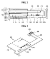
- FIG 2 is a cross-sectional view of the liquid crystal display taken along the line A-A' of FIG 1 .
- a liquid crystal display generally includes a liquid crystal panel 110, an optical sheet 120, a light guide panel 130, a reflective sheet 140, an adhesive layer 150, a flexible printed circuit board 200, a first housing 300, and a second housing 400.
- the liquid crystal panel 110 includes a first display plate 111 that includes gate lines (not shown), data lines (not shown), thin film transistor arrays, and pixel electrodes, a second display plate 112 that includes black matrices and common electrodes, and faces the first display plate 111, a first polarizing plate 113 that is disposed under the first display plate 111, and a second polarizing plate 114 that is disposed on the second display plate 112.
- a liquid crystal layer (not shown) is provided between the first display plate 111 and the second display plate 112.
- the liquid crystal panel 110 including display plates and polarizing plates is disposed inside the first housing 300 (described later).
- the liquid crystal panel 110 may be disposed on the seating step 310 from above the first housing 300.
- a driver integrated circuit 115 for driving the liquid crystal display and the flexible printed circuit board 200 may be disposed at one side of the liquid crystal panel 110.
- the driver integrated circuit 115 is electrically connected with the flexible printed circuit board 200 to receive a driving voltage from the flexible printed circuit board 200.
- the optical sheet 120 is disposed under the liquid crystal panel 110.
- the optical sheet 120 diffuses or concentrates light that passes through the light guide panel 130 from light-source, i.e., point-light-sources 240.
- the optical sheet 120 includes a diffusion sheet 121, a first prism sheet 122, and a second prism sheet 123.
- the diffusion sheet 121 is disposed on the light guide panel 130, and improves luminance and uniformity of luminance of the incident light from the light-source, i.e., point-light-sources 240.
- the first prism sheet 122 and the second prism sheet 123 that concentrate and transmit the light diffused by the diffusion sheet 121 are disposed sequentially on the diffusion sheet 121.
- the second prism sheet 123 may be removed when it is sufficient to ensure the luminance and the viewing angle only with the first prism sheet 122.
- the optical sheet 120 is accommodated inside the first housing 300, together with the liquid crystal panel 110. Specifically, the optical sheet 120 may be in direct contact with the liquid crystal panel 110, on the light guide panel 130. The optical sheet 120, however, may be separated from the liquid crystal panel 110 by a separator (not shown) provided in the first housing 300.
- FIG 3 is a perspective view seen from the bottom of the flexible printed circuit board 200 included in the liquid crystal display according to the first embodiment of the invention.
- a side 210 of the flexible printed circuit board 200 contacts with the liquid crystal panel 110, i.e., the first display plate 111.
- the flexible printed circuit board 200 is bent along the sides 320 and 330 of the first housing (described later), in detail, a first guide groove 320a of the first housing 300, and the other side 220 of the flexible printed circuit board 200 is attached to the lower side of the seating step 310 of the first housing 300.
- the edge of the side 220 of the flexible printed circuit board 200 may be provided with an adhesive layer (not shown), such as double-sided tape, which allows the side 220 of the flexible printed circuit board 200 to adhere to the first housing 300.
- a plurality of driving components 260 are mounted at the side 220 of the flexible printed circuit board 200 for processing all of the gate driving signals and the data driving signals to apply the gate driving signals and data driving signals.
- the flexible printed circuit board 200 is provided with the light-source, i.e., point-light-sources 240 providing light to the liquid crystal display, which is a passive light-emitting device.
- the flexible printed circuit board 200 may have an extension 225 that extends from the side 220 of the flexible printed circuit board and a connector-mounted portion 230 connected to the extension 225. Since the flexible printed circuit board 200 has the extension 225 that extends perpendicularly from the side 220, it has a U-shape.
- the flexible printed circuit board 200 is a film having a predetermined thickness T 1 , and the smaller the thickness T 1 , the more the manufacturing cost increases. Accordingly, the manufacturing cost can be saved by increasing the thickness T 1 of the flexible printed circuit board 200. It is possible to maintain the entire thickness of the liquid crystal display, even though the thickness T 1 of the flexible printed circuit board 200 increases, by adjusting the length L 1 of the flexible printed circuit board 200 such that the side 220 of the flexible printed circuit board 200 does not overlap the reflective sheet 140 (described later). When the length L1 of the flexible printed circuit board 200 is adjusted as described above, the flexible printed circuit board 200 does not overlap the reflective sheet 140 and the adhesive layer 150 for bonding the reflective sheet 140 to the second housing 400. Accordingly, although the thickness T1 of the flexible printed circuit board 200 increases, the entire thickness of the liquid crystal display does not increase as compared with when the flexible printed circuit board 200 overlaps the reflective sheet 140.
- An LED Light Emitted Diode
- the light-source i.e., point-light-sources 240 at the side 220 of the flexible printed circuit board 200.
- the light-source, i.e., point-light-sources 240 are disposed parallel with the side of the light guide panel 130 (described later) and transmit light to the light guide panel 130.
- An external voltage is applied through a connector 250 mounted on the connector-mounted portion 230 of the flexible printed circuit board 200.
- FIG 4 is a perspective view seen from the bottom of the first housing included in the liquid crystal display according to the first embodiment of the invention.
- FIG 5 is a perspective view illustrating the arrangement of the flexible printed circuit board in the first housing according to the first embodiment of the invention.
- the first housing 300 may be a frame with a plurality of sides 320 and 330.
- the first housing 300 may be a rectangular frame.
- the first housing-sides 320 and 330 include first housing-first sides 320 that are longitudinally formed and first housing-second sides 330 that are transversely formed in connection with the first housing sides 320.
- the first housing 300 may be made of a white plastic having good reflection and workability. When the first housing 300 is white, the light that has passed through the light guide panel 130 reflects from the sides 320 and 330 of the first housing 300, which minimizes loss of light. Further, the first housing 300 is made of plastic, so that it is easy to form the seating step 310, the first guide groove 320a, and the second guide groove 330a, which will be described later.
- the first guide groove 320a is formed on one of the first housing sides 320 to guide the bending of the flexible printed circuit board 200.
- the first guide groove 320a may be engraved on the first housing-first side 320 to reduce the height and thickness of the first housing-first side 320. Since the first guide groove 320a is smaller in height and thickness than the first housing-first side 320, when the side 210 of the flexible printed circuit board 200 is disposed along the first guide groove 320a, it is possible to reduce the thickness of the flexible printed circuit board 200 protruding outside the first housing 300.
- the first guide groove 320a overlaps an opening 440 of the second housing 400 (described later) and the flexible printed circuit board 200 is accommodated in the opening 440. Therefore, the other side of the flexible printed circuit board 200 does not overlap the bottom 410 of the second housing 400 (described later).
- the first housing 300 further has the seating step 310 formed along the inside of the sides 320 and 330.
- the first housing 300 formed of the sides 320, 330 is open at the center and the seating step 310 protrudes from the sides 320 and 330 toward the center of the first housing 300.
- the liquid crystal panel 110 and the optical sheet 120 are disposed on the seating step 310 as described above.
- the optical sheet 120 may be disposed on a side of the seating sheet 310, attached to the liquid panel 110.
- the width of a side of the seating sheet 310 adjacent to the first guide groove 320a extends to the center.
- a point-light-source groove 350 and a driving component groove 360 are formed on the lower surface of the width-extended side of the seating sheet 310 to accommodate the point-light-source 240 and a driving component 260 mounted on the side 220 of the flexible printed circuit board 200.
- the first housing-second side 330 may be perpendicular to the first housing-first side 320.
- the first housing-second side 330 has the second guide groove 330a that guides the extension 225 of the flexible printed circuit board 200.
- the extension 225 of the flexible printed circuit board 200 bends in the direction of arrow shown in FIG 5 and overlaps a side 210 of the flexible printed circuit board 200 with the connector 250 facing the lower side of the first housing 300.
- the second guide groove 330a is formed such that it overlaps the opening 440 of the second housing 400 (described later) and the flexible printed circuit board 200 is accommodated in the opening 440. Therefore, the flexible printed circuit board 200 does not overlap the bottom 410 of the second housing 400.
- Fastening protrusions 340 are formed on the first housing-second side 330 to fasten the first housing 300 to the second housing 400.
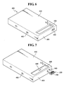
- FIG. 6 is a perspective view seen from the bottom of a second housing 400 included in the liquid crystal display according to the first embodiment of the invention.
- FIG 7 is a perspective view illustrating the arrangement of the flexible printed circuit board in the second housing according to the first embodiment of the invention.
- the optical waveguide 130 is disposed under the first housing 300 and guides light emitted from the point-light-source 240.
- the optical waveguide 130 may be formed of a light transmissive material such as, for example, an acrylic resin such as PMMA (PolyMethyl MethAcrylate), or PC (PolyCarbonate) that has a constant refractive index, in order to effectively guide light.
- a dispersion pattern (not shown) may be provided on a side of the optical waveguide 130 to transmit the light upward that has entered the optical waveguide 130 through a side.
- the reflective sheet 140 is disposed under the optical waveguide 130 and reflects light upward that is transmitted to the second housing 400.
- the adhesive layer 150 is disposed under the reflective sheet 140 to attach the reflective sheet 140 to the bottom 410 of the second housing 400.
- the adhesive layer 150 may be, for example, double-sided tape.
- the second housing 400 accommodates the optical waveguide 130 and the reflective sheet 140 and is fastened to the first housing 300.
- the second housing 400 may be made of a metal at the lowermost of the liquid crystal display to protect the accommodated components, and is also called a "bottom chassis".
- the second housing 400 has the bottom 410 where the reflective sheet 140 adheres and sides 420 that are formed along the edge of the bottom 410, and is fastened to the first housing 300.
- the bottom 410 may be formed in a predetermined thickness T 4 , and the reflective sheet 140 adheres to the bottom 410 and the optical waveguide 130 is supported.
- the opening 440 is formed through a side of the bottom 410.
- the opening 440 is formed by cutting off a portion of the bottom 410.
- the side 220 of the flexible printed circuit board 200 is exposed through the opening 440.
- the side 220 of the flexible printed circuit board 200 is disposed under the first housing 300, and does not overlap the reflective sheet 140 and the adhesive layer 150, so that it is possible to increase the thickness T 1 of the flexible printed circuit board 200 (described above). Further, since the flexible printed circuit board 200 does not overlap the second housing 400 by the opening 440 of the second housing 400, it is possible to increase the thickness T 1 of the flexible printed circuit board 200.
- the thickness T 1 of the flexible printed circuit board 200 can be set such that the flexible printed circuit board 200 does not protrude from the bottom 410 of the second housing 400.
- the thickness T 1 of the flexible printed circuit board 200 is equal to or smaller than the sum of the thickness T 2 of the reflective sheet 140, the thickness T 3 of the adhesive layer 150, and the thickness T 4 of the bottom 410.
- the outside of the bottom 410 of the second housing 400 may be spaced at a predetermined thickness T 5 from the side 220 of the flexible printed circuit board 200.
- the thickness T 1 of the flexible printed circuit board 200 can be increased; therefore, it is correspondingly possible to save the manufacturing cost of the expensive flexible printed circuit board 200. Further, an adhesive layer for fixing the flexible printed circuit board 200 to the second housing 400 is not needed because of the opening 440, so that it is possible to reduce adhesion costs.
- the sides 420 are formed along the edge of the bottom 410 of the second housing 400, and define an accommodating space.
- a connector-mounted portion connection groove 440 is formed at one of the sides 420 of the second housing such that the connector-mounted portion 230 of the flexible printed circuit board 200 protrudes from the inside to the outside of the second housing 400. Accordingly, the connector 250 mounted on the flexible printed circuit board 200 is exposed outside the second housing 400 and drives the liquid crystal display using a voltage applied from the outside.
- fastening grooves 450 may be formed on the sides 420 of the second housing for fastening to the first housing. The fastening protrusions 340 of the first housing 300 are fitted in the fastening grooves 450.
- the upside of the liquid crystal display described above i.e., the upside of the liquid display panel 110, may be protected by a top chassis (not shown) or a separate protection cover in apparatuses such as mobile phones.
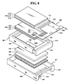
- FIG 8 is an exploded perspective view of a liquid crystal display according to the second embodiment of the invention.
- FIG 9 is a perspective view seen from the bottom of the first housing 301 included in the liquid crystal display according to the second embodiment of the invention.
- FIG 10 is a perspective view illustrating the arrangement of the flexible printed circuit board in the first housing according to the second embodiment of the invention.
- members having the same functions as the members shown in the figures relating to the first embodiment are denoted by the same reference numerals and not described below.
- the liquid crystal display according to the present embodiment has the same configuration as the liquid crystal display according to the first embodiment of the invention except that the structure of the first and second housings and the length of the flexible printed circuit board are partially different.
- the first housing 301 may be a rectangular frame and has a plurality of sides 321 and 330 and a seating step 310 formed along the sides 321 and 330.
- the sides 321 and 330 of the first housing include a first housing-first sides 321 and a first housing-second sides 330.
- a guide groove is not formed on the first housing-first sides 321 according to the present embodiment, unlike the first embodiment. Therefore, it is easy to manufacture the first housing 301.
- the flexible printed circuit board 200 bends along the outside of the first housing-first side 321. For this reason, the length L 2 of the flexible printed circuit board 200 may be larger than the first embodiment.
- a second guide groove 330a that guides the extension 225 of the flexible printed circuit board 200 bending is formed on the first housing-second side 330 adjacent to the first housing-first side 321.
- the extension 225 of the flexible printed circuit board 200 bends in the direction of the arrow, and overlaps a side 210 of the flexible printed circuit board 200.
- the second guide groove 330a prevents the flexible printed circuit board 200 from excessively protruding outside of the first housing-second side 330.
- the second guide groove 330a overlaps an opening 431 (described later), and the flexible printed circuit board 200 is accommodated in the opening 431.
- FIG 11 is a perspective view seen from the bottom of a second housing included in the liquid crystal display according to the second embodiment of the invention.
- FIG 12 is a schematic view illustrating the arrangement of the flexible printed circuit board in the second housing according to the second embodiment of the invention.
- the opening 431 of the second housing 401 extends from the bottom 410 to the side 420 of the second housing.
- the flexible printed circuit board 200 is also disposed under the first housing 301, not overlapping the reflective sheet 140. Further, considering the space defined by the opening 431, it is possible to increase the thickness T 1 of the flexible printed circuit board 200.
- the thickness T 1 of the flexible printed circuit board 200 may be equal to or less than the sum of the thickness of the reflective sheet 140, the thickness of the adhesive layer 150, and the thickness T 4 of the bottom 410.
- the side 220 of the flexible printed circuit board 200 is spaced a predetermined thickness T 5 from the bottom 410 and the outside of the side 420, thereby preventing damage to the flexible printed circuit board 200.
- a connector-mounted portion connection groove 441 is formed at one side of the opening 431 of the side 420 such that the connector-mounted potion 230 of the flexible printed circuit board 200 protrudes outside.
- the liquid crystal display of the embodiments of the invention produces the following effects.
Landscapes
- Physics & Mathematics (AREA)
- Nonlinear Science (AREA)
- Mathematical Physics (AREA)
- Chemical & Material Sciences (AREA)
- Crystallography & Structural Chemistry (AREA)
- General Physics & Mathematics (AREA)
- Optics & Photonics (AREA)
- Liquid Crystal (AREA)
Applications Claiming Priority (1)
| Application Number | Priority Date | Filing Date | Title |
|---|---|---|---|
| KR1020070055623A KR101348247B1 (ko) | 2007-06-07 | 2007-06-07 | 액정 표시 장치 |
Publications (2)
| Publication Number | Publication Date |
|---|---|
| EP2000849A1 true EP2000849A1 (fr) | 2008-12-10 |
| EP2000849B1 EP2000849B1 (fr) | 2010-06-09 |
Family
ID=39687065
Family Applications (1)
| Application Number | Title | Priority Date | Filing Date |
|---|---|---|---|
| EP08009790A Ceased EP2000849B1 (fr) | 2007-06-07 | 2008-05-29 | Affichage à cristaux liquides |
Country Status (6)
| Country | Link |
|---|---|
| US (2) | US7924389B2 (fr) |
| EP (1) | EP2000849B1 (fr) |
| JP (1) | JP5582677B2 (fr) |
| KR (1) | KR101348247B1 (fr) |
| CN (1) | CN101320142B (fr) |
| DE (1) | DE602008001460D1 (fr) |
Cited By (1)
| Publication number | Priority date | Publication date | Assignee | Title |
|---|---|---|---|---|
| JP2024075606A (ja) * | 2009-07-07 | 2024-06-04 | 株式会社半導体エネルギー研究所 | 発光装置 |
Families Citing this family (35)
| Publication number | Priority date | Publication date | Assignee | Title |
|---|---|---|---|---|
| JP4959506B2 (ja) * | 2007-10-31 | 2012-06-27 | 株式会社ジャパンディスプレイイースト | 液晶表示装置 |
| JP5287045B2 (ja) * | 2008-08-29 | 2013-09-11 | サクサ株式会社 | 液晶表示装置 |
| KR101515462B1 (ko) * | 2008-11-13 | 2015-05-06 | 삼성디스플레이 주식회사 | 액정 표시 장치 및 이의 조립 방법 |
| WO2010087240A1 (fr) * | 2009-01-30 | 2010-08-05 | シャープ株式会社 | Boîtier électronique et appareil d'affichage |
| JP5273804B2 (ja) * | 2009-07-13 | 2013-08-28 | 株式会社ジャパンディスプレイ | 表示装置 |
| CN101968579B (zh) * | 2009-07-27 | 2013-01-02 | 群康科技(深圳)有限公司 | 液晶显示器及其组装方法 |
| KR101633105B1 (ko) * | 2009-09-08 | 2016-06-24 | 엘지디스플레이 주식회사 | 액정표시장치 |
| CN102062959B (zh) * | 2009-11-12 | 2013-01-16 | 群康科技(深圳)有限公司 | 液晶显示装置 |
| JP5377269B2 (ja) * | 2009-12-22 | 2013-12-25 | 株式会社ジャパンディスプレイ | 電気光学装置及び電子機器 |
| JP5507237B2 (ja) * | 2009-12-25 | 2014-05-28 | 株式会社ジャパンディスプレイ | 液晶表示装置 |
| TWI389067B (zh) * | 2010-06-29 | 2013-03-11 | Compal Electronics Inc | 顯示模組及其組裝方法 |
| KR101767961B1 (ko) * | 2010-08-31 | 2017-08-16 | 삼성디스플레이 주식회사 | 광공급 어셈블리 및 표시 장치 |
| KR101095122B1 (ko) * | 2010-12-24 | 2011-12-16 | 삼성전기주식회사 | 레이져 네비게이션 모듈 |
| JP5655648B2 (ja) * | 2011-03-15 | 2015-01-21 | 富士通株式会社 | 電子装置及び回路基板の接続構造 |
| CN103364990A (zh) * | 2012-03-30 | 2013-10-23 | 鑫成科技(成都)有限公司 | 液晶显示装置 |
| JP2014026173A (ja) * | 2012-07-27 | 2014-02-06 | Japan Display Inc | 液晶表示装置 |
| KR102046864B1 (ko) | 2013-03-13 | 2019-11-20 | 삼성전자주식회사 | 유연성 디스플레이 장치 |
| JP2014238497A (ja) * | 2013-06-07 | 2014-12-18 | 株式会社ジャパンディスプレイ | 液晶表示装置 |
| KR102039363B1 (ko) * | 2013-06-26 | 2019-11-01 | 엘지디스플레이 주식회사 | 액정표시소자 |
| EA026365B1 (ru) * | 2013-07-25 | 2017-03-31 | Общество с ограниченной ответственностью "ДиС ПЛЮС" | Корпус светодиодного осветительного устройства |
| KR102098304B1 (ko) * | 2013-12-10 | 2020-05-27 | 삼성디스플레이 주식회사 | 액정 표시 장치 및 그 제조 방법 |
| KR101990713B1 (ko) | 2014-09-02 | 2019-06-18 | 선전 로욜 테크놀로지스 컴퍼니 리미티드 | 디스플레이 모듈 및 상기 디스플레이 모듈을 구비하는 전자 장치 |
| JP2017037140A (ja) * | 2015-08-07 | 2017-02-16 | 株式会社ジャパンディスプレイ | 収容ケース、これを備える液晶表示装置 |
| KR102331265B1 (ko) * | 2015-08-31 | 2021-11-26 | 삼성디스플레이 주식회사 | 표시 장치 |
| KR102378723B1 (ko) | 2015-09-21 | 2022-03-28 | 삼성전자주식회사 | 디스플레이 장치 |
| CN105785616A (zh) * | 2016-05-05 | 2016-07-20 | 武汉华星光电技术有限公司 | 液晶显示装置 |
| RU2643526C2 (ru) | 2016-05-17 | 2018-02-02 | Юрий Борисович Соколов | Светодиодный источник освещения с питанием от нестабильной трехфазной сети переменного тока |
| RU2633966C1 (ru) | 2016-11-30 | 2017-10-20 | Юрий Борисович Соколов | Источник питания от многофазной сети переменного тока с коррекцией гармонических колебаний |
| WO2018192370A1 (fr) | 2017-04-17 | 2018-10-25 | Oppo广东移动通信有限公司 | Dispositif d'affichage, équipement électronique, et procédé de fabrication de dispositif d'affichage |
| US10782736B2 (en) | 2018-02-20 | 2020-09-22 | Intel Corporation | Edge-to-edge display devices and related methods |
| CN110012593A (zh) * | 2019-04-18 | 2019-07-12 | 广西天山电子股份有限公司 | 一种柔性电路板及其制备方法、液晶显示模组 |
| US11209131B2 (en) | 2019-04-23 | 2021-12-28 | Lumileds Llc | Alignment features for LED light engine |
| KR102610045B1 (ko) * | 2019-05-10 | 2023-12-06 | 엘지디스플레이 주식회사 | 표시장치 |
| CN113946072B (zh) * | 2021-10-28 | 2024-08-09 | 高创(苏州)电子有限公司 | 背板、背光模组和显示装置 |
| EP4328707A4 (fr) * | 2021-11-29 | 2024-08-07 | Samsung Electronics Co., Ltd. | Ensemble de connexion comprenant une carte de circuit imprimé souple, et dispositif électronique comprenant celui-ci |
Citations (3)
| Publication number | Priority date | Publication date | Assignee | Title |
|---|---|---|---|---|
| US20040263505A1 (en) * | 2003-06-27 | 2004-12-30 | Masaki Tsubokura | Display device |
| US20050179850A1 (en) * | 2004-02-12 | 2005-08-18 | Chang-Lung Du | Liquid crystal display module |
| US20060285353A1 (en) * | 2005-06-17 | 2006-12-21 | Samsung Electronics Co., Ltd. | Liquid crystal display apparatus |
Family Cites Families (27)
| Publication number | Priority date | Publication date | Assignee | Title |
|---|---|---|---|---|
| JP2868502B1 (ja) * | 1998-02-12 | 1999-03-10 | 静岡日本電気株式会社 | 液晶ディスプレー・モジュール |
| JP3594500B2 (ja) * | 1998-11-12 | 2004-12-02 | 松下電器産業株式会社 | 液晶表示器取付接続装置 |
| TWI304909B (fr) * | 2000-10-04 | 2009-01-01 | Matsushita Electric Industrial Co Ltd | |
| US6930737B2 (en) * | 2001-01-16 | 2005-08-16 | Visteon Global Technologies, Inc. | LED backlighting system |
| KR100796487B1 (ko) * | 2001-12-22 | 2008-01-21 | 엘지.필립스 엘시디 주식회사 | 액정표시장치 |
| US7153018B2 (en) * | 2002-09-19 | 2006-12-26 | Matsushita Electric Industrial Co., Ltd. | Illumination unit and liquid crystal display comprising it |
| JP4345337B2 (ja) * | 2003-03-31 | 2009-10-14 | セイコーエプソン株式会社 | 電気光学装置及び電子機器 |
| JP4349009B2 (ja) * | 2003-06-24 | 2009-10-21 | セイコーエプソン株式会社 | 電気光学装置、製造方法及び電子機器 |
| JP2005017964A (ja) | 2003-06-30 | 2005-01-20 | Kawaguchiko Seimitsu Co Ltd | バックライト付液晶表示装置 |
| JP2005099619A (ja) | 2003-09-26 | 2005-04-14 | Seiko Epson Corp | 電気光学装置、およびこの電気光学装置を備えた電子機器 |
| TWI249717B (en) * | 2004-04-19 | 2006-02-21 | Au Optronics Corp | Signal transmission device |
| JP4468061B2 (ja) * | 2004-04-30 | 2010-05-26 | 株式会社 日立ディスプレイズ | 表示装置 |
| JP4196888B2 (ja) * | 2004-06-25 | 2008-12-17 | セイコーエプソン株式会社 | 電気光学装置及び電子機器 |
| JP4572323B2 (ja) * | 2004-07-22 | 2010-11-04 | セイコーエプソン株式会社 | 電気光学装置および電子機器 |
| KR101122216B1 (ko) * | 2004-11-29 | 2012-03-19 | 삼성전자주식회사 | 백라이트 어셈블리 및 표시장치 |
| JP4552637B2 (ja) * | 2004-12-09 | 2010-09-29 | エプソンイメージングデバイス株式会社 | 液晶表示装置 |
| KR20060070343A (ko) | 2004-12-20 | 2006-06-23 | 삼성전자주식회사 | 일체형 섀시를 구비한 평판표시장치 |
| JP2006184383A (ja) * | 2004-12-27 | 2006-07-13 | Seiko Epson Corp | 電気光学装置および電子機器 |
| JP4581726B2 (ja) * | 2004-12-28 | 2010-11-17 | ソニー株式会社 | 表示装置および携帯機器 |
| KR20070000073A (ko) | 2005-06-27 | 2007-01-02 | 삼성전자주식회사 | 표시 장치 |
| JP4679985B2 (ja) * | 2005-07-07 | 2011-05-11 | 株式会社 日立ディスプレイズ | 液晶表示装置 |
| JP4616105B2 (ja) * | 2005-07-20 | 2011-01-19 | 株式会社 日立ディスプレイズ | 液晶表示装置 |
| TWI313374B (en) * | 2005-10-21 | 2009-08-11 | Innolux Display Corp | Liquid crystal display device |
| KR101266506B1 (ko) * | 2005-12-08 | 2013-05-23 | 삼성디스플레이 주식회사 | 표시장치용 보호커버 및 이를 갖는 표시장치 |
| JP4238879B2 (ja) * | 2006-04-03 | 2009-03-18 | エプソンイメージングデバイス株式会社 | 照明装置及び液晶表示装置 |
| JP3129206U (ja) * | 2006-11-27 | 2007-02-08 | 船井電機株式会社 | 液晶モジュール |
| TWM319423U (en) * | 2007-03-05 | 2007-09-21 | Innolux Display Corp | Liquid crystal display |
-
2007
- 2007-06-07 KR KR1020070055623A patent/KR101348247B1/ko not_active Expired - Fee Related
- 2007-10-23 JP JP2007275277A patent/JP5582677B2/ja not_active Expired - Fee Related
-
2008
- 2008-04-17 US US12/148,342 patent/US7924389B2/en active Active
- 2008-05-29 DE DE602008001460T patent/DE602008001460D1/de active Active
- 2008-05-29 EP EP08009790A patent/EP2000849B1/fr not_active Ceased
- 2008-06-06 CN CN2008100859683A patent/CN101320142B/zh not_active Expired - Fee Related
-
2011
- 2011-03-10 US US13/045,296 patent/US8848128B2/en active Active
Patent Citations (3)
| Publication number | Priority date | Publication date | Assignee | Title |
|---|---|---|---|---|
| US20040263505A1 (en) * | 2003-06-27 | 2004-12-30 | Masaki Tsubokura | Display device |
| US20050179850A1 (en) * | 2004-02-12 | 2005-08-18 | Chang-Lung Du | Liquid crystal display module |
| US20060285353A1 (en) * | 2005-06-17 | 2006-12-21 | Samsung Electronics Co., Ltd. | Liquid crystal display apparatus |
Cited By (2)
| Publication number | Priority date | Publication date | Assignee | Title |
|---|---|---|---|---|
| JP2024075606A (ja) * | 2009-07-07 | 2024-06-04 | 株式会社半導体エネルギー研究所 | 発光装置 |
| US12513986B2 (en) | 2009-07-07 | 2025-12-30 | Semiconductor Energy Laboratory Co., Ltd. | Display device |
Also Published As
| Publication number | Publication date |
|---|---|
| CN101320142A (zh) | 2008-12-10 |
| JP5582677B2 (ja) | 2014-09-03 |
| US20080303972A1 (en) | 2008-12-11 |
| DE602008001460D1 (de) | 2010-07-22 |
| KR20080107633A (ko) | 2008-12-11 |
| US8848128B2 (en) | 2014-09-30 |
| KR101348247B1 (ko) | 2014-01-09 |
| JP2008304887A (ja) | 2008-12-18 |
| CN101320142B (zh) | 2012-08-29 |
| US20110164199A1 (en) | 2011-07-07 |
| US7924389B2 (en) | 2011-04-12 |
| EP2000849B1 (fr) | 2010-06-09 |
Similar Documents
| Publication | Publication Date | Title |
|---|---|---|
| US7924389B2 (en) | Liquid crystal display with housing exposed flexible printed circuit | |
| US9442244B2 (en) | Liquid crystal display | |
| US7898614B2 (en) | Liquid crystal display module with flexible printed circuit board, insulation sheet and reflection sheet | |
| US7557888B2 (en) | Liquid crystal display device | |
| US6806920B2 (en) | Liquid crystal display apparatus | |
| US7377682B2 (en) | Backlight module and liquid crystal display device using the same | |
| US10254470B2 (en) | Display device and method of manufacturing the same | |
| EP2126624B1 (fr) | Afficheur comprenant un châssis formé d'une plaque métallique pliée | |
| US20080079863A1 (en) | Liquid Crystal Display Device | |
| US7784990B2 (en) | Light source unit, light emitting device, and display device having same | |
| CN100474358C (zh) | 平面显示装置 | |
| US20130016303A1 (en) | Liquid crystal display device and electronic device | |
| US20150366082A1 (en) | Display device | |
| US8696182B2 (en) | Display device and backlight unit for improving uniformity of brightness | |
| JP2002258249A (ja) | 液晶表示装置及びその組み立て方法 | |
| KR101737799B1 (ko) | 차광테이프와 이를 적용한 백라이트 유닛 및 이를 구비한 액정표시장치 | |
| US10551555B2 (en) | Backlight unit restricting substrate movement and display apparatus including the same | |
| KR101279242B1 (ko) | 액정표시장치 | |
| KR20070114473A (ko) | 표시장치 |
Legal Events
| Date | Code | Title | Description |
|---|---|---|---|
| PUAI | Public reference made under article 153(3) epc to a published international application that has entered the european phase |
Free format text: ORIGINAL CODE: 0009012 |
|
| AK | Designated contracting states |
Kind code of ref document: A1 Designated state(s): AT BE BG CH CY CZ DE DK EE ES FI FR GB GR HR HU IE IS IT LI LT LU LV MC MT NL NO PL PT RO SE SI SK TR |
|
| AX | Request for extension of the european patent |
Extension state: AL BA MK RS |
|
| 17P | Request for examination filed |
Effective date: 20090608 |
|
| 17Q | First examination report despatched |
Effective date: 20090708 |
|
| AKX | Designation fees paid |
Designated state(s): DE GB IT NL |
|
| GRAP | Despatch of communication of intention to grant a patent |
Free format text: ORIGINAL CODE: EPIDOSNIGR1 |
|
| GRAS | Grant fee paid |
Free format text: ORIGINAL CODE: EPIDOSNIGR3 |
|
| GRAA | (expected) grant |
Free format text: ORIGINAL CODE: 0009210 |
|
| AK | Designated contracting states |
Kind code of ref document: B1 Designated state(s): DE GB IT NL |
|
| REF | Corresponds to: |
Ref document number: 602008001460 Country of ref document: DE Date of ref document: 20100722 Kind code of ref document: P |
|
| REG | Reference to a national code |
Ref country code: NL Ref legal event code: T3 |
|
| PLBE | No opposition filed within time limit |
Free format text: ORIGINAL CODE: 0009261 |
|
| STAA | Information on the status of an ep patent application or granted ep patent |
Free format text: STATUS: NO OPPOSITION FILED WITHIN TIME LIMIT |
|
| REG | Reference to a national code |
Ref country code: DE Ref legal event code: R097 Ref document number: 602008001460 Country of ref document: DE Effective date: 20110309 |
|
| REG | Reference to a national code |
Ref country code: NL Ref legal event code: SD Effective date: 20121017 |
|
| REG | Reference to a national code |
Ref country code: GB Ref legal event code: 732E Free format text: REGISTERED BETWEEN 20130307 AND 20130313 |
|
| REG | Reference to a national code |
Ref country code: DE Ref legal event code: R082 Ref document number: 602008001460 Country of ref document: DE Representative=s name: DR. WEITZEL & PARTNER, DE |
|
| REG | Reference to a national code |
Ref country code: DE Ref legal event code: R081 Ref document number: 602008001460 Country of ref document: DE Owner name: SAMSUNG DISPLAY CO., LTD., KR Free format text: FORMER OWNER: SAMSUNG ELECTRONICS CO., LTD., SUWON-SI, KR Effective date: 20130422 Ref country code: DE Ref legal event code: R082 Ref document number: 602008001460 Country of ref document: DE Representative=s name: DR. WEITZEL & PARTNER, DE Effective date: 20130422 Ref country code: DE Ref legal event code: R082 Ref document number: 602008001460 Country of ref document: DE Representative=s name: DR. WEITZEL & PARTNER PATENT- UND RECHTSANWAEL, DE Effective date: 20130422 Ref country code: DE Ref legal event code: R081 Ref document number: 602008001460 Country of ref document: DE Owner name: SAMSUNG DISPLAY CO., LTD., YONGIN-CITY, KR Free format text: FORMER OWNER: SAMSUNG ELECTRONICS CO., LTD., SUWON-SI, GYEONGGI-DO, KR Effective date: 20130422 |
|
| PGFP | Annual fee paid to national office [announced via postgrant information from national office to epo] |
Ref country code: DE Payment date: 20200506 Year of fee payment: 13 Ref country code: NL Payment date: 20200507 Year of fee payment: 13 |
|
| PGFP | Annual fee paid to national office [announced via postgrant information from national office to epo] |
Ref country code: GB Payment date: 20200511 Year of fee payment: 13 Ref country code: IT Payment date: 20200511 Year of fee payment: 13 |
|
| REG | Reference to a national code |
Ref country code: DE Ref legal event code: R119 Ref document number: 602008001460 Country of ref document: DE |
|
| REG | Reference to a national code |
Ref country code: NL Ref legal event code: MM Effective date: 20210601 |
|
| GBPC | Gb: european patent ceased through non-payment of renewal fee |
Effective date: 20210529 |
|
| PG25 | Lapsed in a contracting state [announced via postgrant information from national office to epo] |
Ref country code: GB Free format text: LAPSE BECAUSE OF NON-PAYMENT OF DUE FEES Effective date: 20210529 Ref country code: DE Free format text: LAPSE BECAUSE OF NON-PAYMENT OF DUE FEES Effective date: 20211201 |
|
| PG25 | Lapsed in a contracting state [announced via postgrant information from national office to epo] |
Ref country code: NL Free format text: LAPSE BECAUSE OF NON-PAYMENT OF DUE FEES Effective date: 20210601 |
|
| PG25 | Lapsed in a contracting state [announced via postgrant information from national office to epo] |
Ref country code: IT Free format text: LAPSE BECAUSE OF NON-PAYMENT OF DUE FEES Effective date: 20200529 |
|
| PG25 | Lapsed in a contracting state [announced via postgrant information from national office to epo] |
Ref country code: IT Free format text: LAPSE BECAUSE OF NON-PAYMENT OF DUE FEES Effective date: 20210529 |