EP2001045A1 - Appareil cvd a plasma, procede de formation de film mince et dispositif a semi-conducteurs - Google Patents
Appareil cvd a plasma, procede de formation de film mince et dispositif a semi-conducteurs Download PDFInfo
- Publication number
- EP2001045A1 EP2001045A1 EP07739394A EP07739394A EP2001045A1 EP 2001045 A1 EP2001045 A1 EP 2001045A1 EP 07739394 A EP07739394 A EP 07739394A EP 07739394 A EP07739394 A EP 07739394A EP 2001045 A1 EP2001045 A1 EP 2001045A1
- Authority
- EP
- European Patent Office
- Prior art keywords
- compound
- plasma
- reaction chamber
- substrate
- film
- Prior art date
- Legal status (The legal status is an assumption and is not a legal conclusion. Google has not performed a legal analysis and makes no representation as to the accuracy of the status listed.)
- Granted
Links
Images

Classifications
-
- C—CHEMISTRY; METALLURGY
- C23—COATING METALLIC MATERIAL; COATING MATERIAL WITH METALLIC MATERIAL; CHEMICAL SURFACE TREATMENT; DIFFUSION TREATMENT OF METALLIC MATERIAL; COATING BY VACUUM EVAPORATION, BY SPUTTERING, BY ION IMPLANTATION OR BY CHEMICAL VAPOUR DEPOSITION, IN GENERAL; INHIBITING CORROSION OF METALLIC MATERIAL OR INCRUSTATION IN GENERAL
- C23C—COATING METALLIC MATERIAL; COATING MATERIAL WITH METALLIC MATERIAL; SURFACE TREATMENT OF METALLIC MATERIAL BY DIFFUSION INTO THE SURFACE, BY CHEMICAL CONVERSION OR SUBSTITUTION; COATING BY VACUUM EVAPORATION, BY SPUTTERING, BY ION IMPLANTATION OR BY CHEMICAL VAPOUR DEPOSITION, IN GENERAL
- C23C16/00—Chemical coating by decomposition of gaseous compounds, without leaving reaction products of surface material in the coating, i.e. chemical vapour deposition [CVD] processes
- C23C16/22—Chemical coating by decomposition of gaseous compounds, without leaving reaction products of surface material in the coating, i.e. chemical vapour deposition [CVD] processes characterised by the deposition of inorganic material, other than metallic material
- C23C16/30—Deposition of compounds, mixtures or solid solutions, e.g. borides, carbides, nitrides
-
- C—CHEMISTRY; METALLURGY
- C23—COATING METALLIC MATERIAL; COATING MATERIAL WITH METALLIC MATERIAL; CHEMICAL SURFACE TREATMENT; DIFFUSION TREATMENT OF METALLIC MATERIAL; COATING BY VACUUM EVAPORATION, BY SPUTTERING, BY ION IMPLANTATION OR BY CHEMICAL VAPOUR DEPOSITION, IN GENERAL; INHIBITING CORROSION OF METALLIC MATERIAL OR INCRUSTATION IN GENERAL
- C23C—COATING METALLIC MATERIAL; COATING MATERIAL WITH METALLIC MATERIAL; SURFACE TREATMENT OF METALLIC MATERIAL BY DIFFUSION INTO THE SURFACE, BY CHEMICAL CONVERSION OR SUBSTITUTION; COATING BY VACUUM EVAPORATION, BY SPUTTERING, BY ION IMPLANTATION OR BY CHEMICAL VAPOUR DEPOSITION, IN GENERAL
- C23C16/00—Chemical coating by decomposition of gaseous compounds, without leaving reaction products of surface material in the coating, i.e. chemical vapour deposition [CVD] processes
- C23C16/22—Chemical coating by decomposition of gaseous compounds, without leaving reaction products of surface material in the coating, i.e. chemical vapour deposition [CVD] processes characterised by the deposition of inorganic material, other than metallic material
- C23C16/30—Deposition of compounds, mixtures or solid solutions, e.g. borides, carbides, nitrides
- C23C16/34—Nitrides
- C23C16/342—Boron nitride
-
- C—CHEMISTRY; METALLURGY
- C23—COATING METALLIC MATERIAL; COATING MATERIAL WITH METALLIC MATERIAL; CHEMICAL SURFACE TREATMENT; DIFFUSION TREATMENT OF METALLIC MATERIAL; COATING BY VACUUM EVAPORATION, BY SPUTTERING, BY ION IMPLANTATION OR BY CHEMICAL VAPOUR DEPOSITION, IN GENERAL; INHIBITING CORROSION OF METALLIC MATERIAL OR INCRUSTATION IN GENERAL
- C23C—COATING METALLIC MATERIAL; COATING MATERIAL WITH METALLIC MATERIAL; SURFACE TREATMENT OF METALLIC MATERIAL BY DIFFUSION INTO THE SURFACE, BY CHEMICAL CONVERSION OR SUBSTITUTION; COATING BY VACUUM EVAPORATION, BY SPUTTERING, BY ION IMPLANTATION OR BY CHEMICAL VAPOUR DEPOSITION, IN GENERAL
- C23C16/00—Chemical coating by decomposition of gaseous compounds, without leaving reaction products of surface material in the coating, i.e. chemical vapour deposition [CVD] processes
- C23C16/44—Chemical coating by decomposition of gaseous compounds, without leaving reaction products of surface material in the coating, i.e. chemical vapour deposition [CVD] processes characterised by the method of coating
- C23C16/50—Chemical coating by decomposition of gaseous compounds, without leaving reaction products of surface material in the coating, i.e. chemical vapour deposition [CVD] processes characterised by the method of coating using electric discharges
- C23C16/511—Chemical coating by decomposition of gaseous compounds, without leaving reaction products of surface material in the coating, i.e. chemical vapour deposition [CVD] processes characterised by the method of coating using electric discharges using microwave discharges
-
- H—ELECTRICITY
- H01—ELECTRIC ELEMENTS
- H01J—ELECTRIC DISCHARGE TUBES OR DISCHARGE LAMPS
- H01J37/00—Discharge tubes with provision for introducing objects or material to be exposed to the discharge, e.g. for the purpose of examination or processing thereof
- H01J37/32—Gas-filled discharge tubes
- H01J37/32431—Constructional details of the reactor
- H01J37/32532—Electrodes
-
- H—ELECTRICITY
- H10—SEMICONDUCTOR DEVICES; ELECTRIC SOLID-STATE DEVICES NOT OTHERWISE PROVIDED FOR
- H10P—GENERIC PROCESSES OR APPARATUS FOR THE MANUFACTURE OR TREATMENT OF DEVICES COVERED BY CLASS H10
- H10P14/00—Formation of materials, e.g. in the shape of layers or pillars
- H10P14/60—Formation of materials, e.g. in the shape of layers or pillars of insulating materials
- H10P14/66—Formation of materials, e.g. in the shape of layers or pillars of insulating materials characterised by the type of materials
- H10P14/668—Formation of materials, e.g. in the shape of layers or pillars of insulating materials characterised by the type of materials the materials being characterised by the deposition precursor materials
-
- H—ELECTRICITY
- H10—SEMICONDUCTOR DEVICES; ELECTRIC SOLID-STATE DEVICES NOT OTHERWISE PROVIDED FOR
- H10P—GENERIC PROCESSES OR APPARATUS FOR THE MANUFACTURE OR TREATMENT OF DEVICES COVERED BY CLASS H10
- H10P14/00—Formation of materials, e.g. in the shape of layers or pillars
- H10P14/60—Formation of materials, e.g. in the shape of layers or pillars of insulating materials
- H10P14/63—Formation of materials, e.g. in the shape of layers or pillars of insulating materials characterised by the formation processes
- H10P14/6326—Deposition processes
- H10P14/6328—Deposition from the gas or vapour phase
- H10P14/6334—Deposition from the gas or vapour phase using decomposition or reaction of gaseous or vapour phase compounds, i.e. chemical vapour deposition
- H10P14/6336—Deposition from the gas or vapour phase using decomposition or reaction of gaseous or vapour phase compounds, i.e. chemical vapour deposition in the presence of a plasma [PECVD]
-
- H—ELECTRICITY
- H10—SEMICONDUCTOR DEVICES; ELECTRIC SOLID-STATE DEVICES NOT OTHERWISE PROVIDED FOR
- H10P—GENERIC PROCESSES OR APPARATUS FOR THE MANUFACTURE OR TREATMENT OF DEVICES COVERED BY CLASS H10
- H10P14/00—Formation of materials, e.g. in the shape of layers or pillars
- H10P14/60—Formation of materials, e.g. in the shape of layers or pillars of insulating materials
- H10P14/68—Organic materials, e.g. photoresists
Definitions
- the present invention relates to a plasma CVD (Chemical Vapor Deposition) apparatus that forms a thin film by using a compound having a borazine skeleton as a raw material.
- the present invention also relates to a thin-film forming method for forming a thin film by using such a compound having a borazine skeleton as a raw material.
- the present invention relates to a semiconductor device that is provided with a thin film formed by this thin-film forming method as an insulating film.
- the signal delay is represented by the product of the resistance value of wiring and the capacity between wirings as well as between layers, and in order to suppress the signal delay to the minimum, effective methods are to reduce the wiring resistance and also to lower the dielectric constant of an interlayer insulating film.
- the present invention has been devised to solve the above-mentioned technical problems, and an objective thereof is to provide a plasma CVD apparatus and a thin-film forming method that can produce a thin film wherein low dielectric constant and high mechanical strength are stably maintained for a long time and insulating characteristics are secured.
- a plasma CVD apparatus is provided with: a reaction chamber having an inlet used for supplying a compound having a borazine skeleton; a feeding electrode, arranged within the reaction chamber, for supporting a substrate and being applied with a negative charge; and plasma generator, arranged opposite to the feeding electrode via the substrate, for generating a plasma within the reaction chamber.
- a thin-film forming method is provided with the steps of: introducing a compound having a borazine skeleton into a reaction chamber; applying a negative charge to a feeding electrode that supports a substrate placed inside the reaction chamber; generating a plasma inside the reaction chamber by using a plasma generator arranged opposite to the feeding electrode via the substrate so that the compound is excited; and sweeping the excited compound by the negative charge to be successively bonded to one another so that the resulting polymerized compound is deposited on the substrate.
- a semiconductor device is provided with an insulating film formed on a substrate by using the thin-film forming method of the present invention, with wiring being further installed thereon.
- the plasma CVD apparatus of the present invention makes it possible to provide a thin film wherein low dielectric constant and high mechanical strength are stably maintained for a long time and insulating characteristics are secured.
- the thin-film forming method of the present invention makes it possible to form a thin film wherein low dielectric constant and high mechanical strength are stably maintained for a long time and insulating characteristics are secured.
- the semiconductor device of the present invention makes it possible to suppress a signal delay to a minimal level, and consequently to achieve a high speed device.
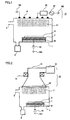
- Fig. 1 is a schematic view that shows a schematic structure of a plasma CVD apparatus (hereinafter, referred to as a PCVD apparatus) in accordance with Embodiment 1 of the present invention.
- the PCVD apparatus in accordance with the present invention is provided with a reaction chamber having a vacuum pump 4 and a material inlet 5 used for supplying a compound having a borazine skeleton, a feeding electrode 7 that is installed in reaction chamber 1 to support a substrate 8, and that is applied with a negative charge, and a plasma generator 12 that is arranged opposite to feeding electrode 7 via substrate 8 so as to generate a plasma 11 within reaction chamber 1.
- a compound having a borazine skeleton is introduced into reaction chamber 1, with a plasma being generated within reaction chamber 1 by plasma generator 12 placed opposite to feeding electrode 7, so that the compound is excited, and by further applying a negative charge to feeding electrode 7, the excited compound is swept toward substrate 8 side, and successively bonded to one another to be polymerized and deposited on substrate 8.
- Plasma generator 12 may be configured by a high frequency power supply 22, a matching device 32 and an antenna 9 having a winding coil structure.
- a high frequency energy, generated by high frequency power supply 22, is adjusted by matching device 32, and propagated into reaction chamber 1 by antenna 9 so that a material gas and the like inside reaction chamber 1 are excited to generate a plasma.
- a magnetic field is generated by antenna 9 having the winding coil structure, and by resonating the magnetic field, the plasma density may be increased.
- the shape of antenna 9 the plasma generating position may be changed.
- one portion of the above-mentioned structure may be omitted depending on circumstances.
- earthed electrodes 102 and 103 are preferably installed.
- the method for applying a negative charge to feeding electrode 7 is performed by connecting a DC power supply 10 to feeding electrode 7.
- earthed electrode 101 is preferably installed.
- the voltage of DC power supply 10 is preferably set to 1500 V or less. When the voltage exceeds 1500 V, the borazine skeleton in a film formed on substrate 8 is damaged, and a component that causes a high dielectric constant, such as boron nitride, is consequently generated, with the result that the leak current of the film increases to impair the insulating characteristic.
- the compound to which the plasma energy has been given is brought into a reaction active state, with the borazine skeleton being maintained therein, and it is consequently drawn toward substrate 8 by a dc electric field applied to feeding electrode 7, with its reaction active state being maintained, so that the active component is sufficiently subjected to a cross-linking reaction. Moreover, since the adjustment of plasma energy is easily carried out, the borazine skeleton is prevented from being decomposed beyond a necessary level so that a desired structure can be maintained.
- the high frequency generated by the above-mentioned high frequency power supply 22 is set to, for example, 13.56 MHz, and is desirably set within a range from 2 GHz to 4 kHz. Moreover, the power is desirably set in a range from 5 to 4000 W. In a case where the power exceeds 4000 W, the decomposing frequency of a compound having a borazine skeleton increases, making it difficult to obtain a desirable borazine skeleton. Preferably, the power is set from 10 W or more to 3000 W or less.
- RF (10 kHz to 1 GHz) or microwaves (1 GHz to 10 GHz) may be used as the high frequency to be applied.
- a plurality of frequencies may be combined.
- Plasma generator 12 may have a structure as shown in Fig. 2 .
- Microwaves, generated by microwave generator 13, are propagated through a waveguide tube 14, and further propagated to the inside of reaction chamber 1 through microwave guide window 16 to be given to a material gas so that a plasma is generated.
- the plasma density may be increased by generating a magnetic field from coil 15.
- the film deposited by heat is further crosslinked to be highly polymerized; thus, it is possible to improve the heat resistance of the film.
- the heat crosslinking process makes it possible to reduce outgas generated from a film after the film forming process, and consequently to reduce limitations in the succeeding processes; therefore, the process is preferably used.
- the material gas temperature and the substrate temperature are preferably controlled within a range from room temperature to 450 °C. In a case where the material gas and the substrate temperature exceed 450 °C, it takes an extremely long period of time to obtain a desired film thickness, with the result that it sometimes becomes difficult to execute the film forming process smoothly.
- the temperatures are preferably set in a range from 50 °C or more to 400 °C or less.
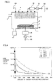
- Control of the above-mentioned substrate temperature may be carried out by on-off operations of heating device 61, or by using a heating/cooling device 62, as shown in Fig. 3 , that also has a cooling function instead of heating device 61, the substrate may be set to a predetermined process temperature.
- Feeding electrode 7 on which substrate 8 is placed may be prepared as a plasma source used for inducing plasma. More specifically, as shown in Fig. 3 , a power supply may be configured by a high frequency power supply 21 in which a negative charge is multiplexed and a matching device 31. Since this structure makes it possible to control an activating reaction on the surface of substrate 8 by using a plasma on the substrate 8 side, the film quality can be controlled.
- the high frequency generated by high frequency power supply 21 for example, 13.56 MHz may be used, and RF (10 kHz to 1 GHz) or microwaves (1 GHz to 10 GHz) may be used as the high frequency. A plurality of frequencies may be combined with one another.
- the power is preferably set to 3000 W or less. When the power exceeds 3000 W, the borazine skeleton in the film formed on substrate 8 is damaged, and a component that causes a high dielectric constant, such as boron nitride, is consequently generated, with the result that the leak current of the film increases to impair the insulating characteristic.
- the introduction of a compound having a borazine skeleton into reaction chamber 1 may be carried out by directing the corresponding compound in a gas state, as it is, thereto through material inlet 5, or may be carried out by processes in which the corresponding compound is evaporated by using a heating evaporator mechanism or the like attached separately, and directed thereto.
- the gas may be introduced by utilizing this evaporating pressure.
- a gas such as Ar, He, nitrogen or the like may be used as a carrier gas.
- the characteristics of the film may be controlled by mixing methane, ethane, ethylene, acetylene, ammonia or a compound of any of alkyl amines therewith.
- the flow rate of the carrier gas is preferably set in a range from about 100 to about 1000 sccm
- the gas flow rate of a material compound having a borazine skeleton is preferably set in a range from 1 to 300 sccm
- the flow rate of methane, ethane, ethylene, acetylene, ammonia or alkyl amines to be added is preferably set in a range from 0 to about 100 sccm.
- the flow rate of the carrier gas is less than 100 sccm, it takes an extremely long period of time to obtain a desired film thickness, with the result that it sometimes becomes difficult to execute the film forming process smoothly.
- the evenness of the film thickness within the substrate face tends to deteriorate.
- the flow rate is more preferably set in a range from 200 sccm or more to 800 sccm or less.
- the flow rate of the material gas is less than 1 sccm, it takes an extremely long period of time to obtain a desired film thickness, with the result that it sometimes becomes difficult to execute the film forming process smoothly.
- the flow rate exceeds 300 sccm, the resulting film has a low crosslinking density to cause a reduction in mechanical strength.
- the flow rate is preferably set from 5 sccm or more to 200 sccm or less.
- the flow rate exceeding 100 sccm causes an increase in the dielectric constant of the resulting film. More preferably, the flow rate is set from 5 sccm or more to 100 sccm or less.
- the pressure of reaction chamber 1 is preferably set to 0.01 Pa or more to 10 Pa or less.
- the pressure is less than 0.01 Pa, the decomposing frequency due to plasma of a compound having a borazine skeleton increases, making it difficult to obtain a desirable borazine skeleton.
- the pressure exceeding 10 Pa causes a film having a low crosslinking density and the subsequent reduction in the mechanical strength. More preferably, the pressure is set to 5 Pa or more to 6.7 Pa or less.
- the pressure may be adjusted by a pressure adjusting device, such as a vacuum pump, or the gas flow rate.
- a partition plate that can sweep ions and block radicals may be formed on substrate 8.
- the radical components in the film absorb moisture after the film formation to give adverse influences to the moisture resistance of the film. By installing the partition plate, it becomes possible to restrain the radical components from being incorporated in the film.
- the present embodiment has exemplified a structure in which feeding electrode 7 is installed on the lower portion of reaction chamber 1, with plasma generator 12 being installed on the upper portion thereof; however, the present invention is not intended to be limited by this structure, as long as feeding electrode 7 and plasma generator 12 are placed opposite to each other.
- the upside-down reversed structure may be used, or these may be placed on side faces of reaction chamber 1.
- the material gas composition having a borazine skeleton
- the carrier gas are formed into ions and radicals in reaction chamber 1.
- the ions are drawn by the electrode having a potential reversed to the charge of their own, and collide therewith repeatedly to react with each other.
- a negative charge is applied to feeding electrode 7 at this time, cations are selectively drawn onto the feeding electrode 7 side, and a film is subsequently formed so that it is possible to reduce the rate of anions and radicals devoting to the film formation.
- a film that is superior in moisture resistance and can maintain stable characteristics even after a lapse of time. More specifically, in comparison with a film formed by a conventional thin-film forming method that can maintain a dielectric constant in a range from 3.0 to 1.8 only for several days, a film, formed by using the thin-film forming method in accordance with the present invention, makes it possible to maintain the corresponding dielectric constant for at least several years.
- such a low dielectric constant can be confirmed by measuring the dielectric constant of a film that has been preserved for a predetermined period of time by using the same method as the method used immediately after the film formation.
- a film formed by using the thin-film forming method according to the present invention hardly contains excessively decomposed matters of boron nitride or the like in comparison with a film formed by using a conventional thin-film forming method, it is possible to achieve a lower dielectric constant. Moreover, since the amount of outgas is reduced, another advantage is that no problems arise in the succeeding semiconductor device manufacturing processes after the film formation.
- any conventionally known compound may be used without limitations as long as it has a borazine structure, and in particular, from the viewpoint of manufacturing a film in which the dielectric constant, thermal expansion coefficient, heat resistance, thermal conductivity and mechanical strength are improved, a compound indicated by the following formula (I) is preferably used as the raw material.
- substituents indicated by R 1 to R 6 may be the same or different from one other, and any of a hydrogen atom or an alkyl group, an alkenyl group or an alkynyl group having carbon atoms of 1 to 4, may be used as those substituents independently.
- all the R 1 to R 6 are not hydrogen atoms.
- boron-hydrogen bonds or nitrogen-hydrogen bonds tend to remain in a film. Since these bonds have a high hydrophilic property, a problem tends to arise in that the moisture absorbing property of the film becomes higher to cause a failure to provide a desired film.
- R 1 to R 6 of the above-mentioned compound (I) when the number of carbon atoms exceeds 4, the content of carbon atoms in the film thus formed becomes higher to cause the possibility of degradation in the heat resistance and mechanical strength in the film.
- the number of carbon atoms is preferably set to 1 or 2.
- a film formed by the thin-film forming method shown in the above-mentioned Embodiment 2 was used as an insulating layer and a wiring pattern made of copper was formed thereon, and these processes were repeated so that a semiconductor device having several laminated layers was manufactured.
- Fig. 5 is a schematic cross-sectional view showing one example of the semiconductor device. Insulating films 502 and 509, a first insulating layer 503, a second insulating layer 505 and a third insulating layer 507 were formed by using the PCVD apparatus shown in the above-mentioned Embodiment 1 through the thin-film forming method in accordance with the above-mentioned Embodiment 2.
- Substrate 8 was heated by a heating device 61 to a temperature of 300 °C, and a dc electric field of - 600 V to - 200 V (Examples 1 to 3) was applied to feeding electrode 7 supporting substrate 8 by DC power supply 10. Furthermore, a high frequency of 13.56 MHz was directed thereto through an antenna 9 at 1000 W so that a plasma 11 was generated; thus, the activated material gas was deposited so that a film was formed. Here, the pressure inside the reaction chamber was maintained at 2 Pa.
- a film forming process was carried out with no dc electric field (0 V) being applied to feeding electrode 7.
- the other conditions are the same as those of the above-mentioned Examples 1 to 3.
- Table 1 indicates that when the applied power from high frequency power supply 22 is raised, the amount of change in dielectric constant corresponding to the amount of change with time can be reduced. However, this also indicates that under the condition that the amount of change in dielectric constant can be reduced, the leak current value increases to cause degradation in the film insulating characteristic.
- a dc electric field Examples 1 to 3
- desirable conditions can be set within ranges of the applied voltage of - 600 V to - 200 V and the applied power of 250 to 1500 W.
Landscapes
- Chemical & Material Sciences (AREA)
- Engineering & Computer Science (AREA)
- Mechanical Engineering (AREA)
- Chemical Kinetics & Catalysis (AREA)
- General Chemical & Material Sciences (AREA)
- Materials Engineering (AREA)
- Metallurgy (AREA)
- Organic Chemistry (AREA)
- Physics & Mathematics (AREA)
- Plasma & Fusion (AREA)
- Inorganic Chemistry (AREA)
- Analytical Chemistry (AREA)
- Chemical Vapour Deposition (AREA)
- Formation Of Insulating Films (AREA)
Applications Claiming Priority (2)
| Application Number | Priority Date | Filing Date | Title |
|---|---|---|---|
| JP2006092017A JP4497323B2 (ja) | 2006-03-29 | 2006-03-29 | プラズマcvd装置 |
| PCT/JP2007/055953 WO2007116644A1 (fr) | 2006-03-29 | 2007-03-23 | Appareil cvd a plasma, procede de formation de film mince et dispositif a semi-conducteurs |
Publications (3)
| Publication Number | Publication Date |
|---|---|
| EP2001045A1 true EP2001045A1 (fr) | 2008-12-10 |
| EP2001045A4 EP2001045A4 (fr) | 2010-02-17 |
| EP2001045B1 EP2001045B1 (fr) | 2017-06-14 |
Family
ID=38580943
Family Applications (1)
| Application Number | Title | Priority Date | Filing Date |
|---|---|---|---|
| EP07739394.0A Ceased EP2001045B1 (fr) | 2006-03-29 | 2007-03-23 | Procédé de formation de film mince et dispositif à semi-conducteurs |
Country Status (7)
| Country | Link |
|---|---|
| US (2) | US8404314B2 (fr) |
| EP (1) | EP2001045B1 (fr) |
| JP (1) | JP4497323B2 (fr) |
| KR (1) | KR101057252B1 (fr) |
| CN (1) | CN101410958B (fr) |
| TW (1) | TWI380351B (fr) |
| WO (1) | WO2007116644A1 (fr) |
Cited By (1)
| Publication number | Priority date | Publication date | Assignee | Title |
|---|---|---|---|---|
| US8288294B2 (en) | 2008-06-30 | 2012-10-16 | Mitsubishi Heavy Industries, Ltd. | Insulating film for semiconductor device, process and apparatus for producing insulating film for semiconductor device, semiconductor device, and process for producing the semiconductor device |
Families Citing this family (11)
| Publication number | Priority date | Publication date | Assignee | Title |
|---|---|---|---|---|
| US8084105B2 (en) * | 2007-05-23 | 2011-12-27 | Applied Materials, Inc. | Method of depositing boron nitride and boron nitride-derived materials |
| JP5760781B2 (ja) | 2011-07-13 | 2015-08-12 | 住友化学株式会社 | 有害節足動物防除組成物及び有害節足動物の防除方法 |
| JP5694543B2 (ja) | 2011-09-08 | 2015-04-01 | 東芝三菱電機産業システム株式会社 | プラズマ発生装置、cvd装置およびプラズマ処理粒子生成装置 |
| WO2013035375A1 (fr) | 2011-09-09 | 2013-03-14 | 東芝三菱電機産業システム株式会社 | Générateur de plasma et dispositif cvd |
| JP5613641B2 (ja) * | 2011-09-12 | 2014-10-29 | 東芝三菱電機産業システム株式会社 | プラズマ発生装置およびcvd装置 |
| CN103887139B (zh) * | 2014-04-08 | 2017-01-11 | 苏州大学 | 用于制备低介电常数材料的等离子增强化学气相沉积装置 |
| CN106797698B (zh) | 2014-07-25 | 2019-11-15 | 东芝三菱电机产业系统株式会社 | 原子团气体产生系统 |
| US11007497B2 (en) | 2014-10-29 | 2021-05-18 | Toshiba Mitsubishi-Electric Industrial Systems Corporation | Gas jetting apparatus |
| WO2016067379A1 (fr) | 2014-10-29 | 2016-05-06 | 東芝三菱電機産業システム株式会社 | Appareil permettant l'injection de gaz dans un appareil de formation de film |
| CN107079575B (zh) | 2014-10-29 | 2020-08-04 | 东芝三菱电机产业系统株式会社 | 放电发生装置 |
| EP3425852B1 (fr) | 2016-02-29 | 2022-03-02 | Audio-Technica Corporation | Système de conférence |
Family Cites Families (25)
| Publication number | Priority date | Publication date | Assignee | Title |
|---|---|---|---|---|
| US5518780A (en) | 1994-06-16 | 1996-05-21 | Ford Motor Company | Method of making hard, transparent amorphous hydrogenated boron nitride films |
| JPH08339992A (ja) | 1995-06-13 | 1996-12-24 | Toshiba Corp | 薄膜形成装置および薄膜形成方法 |
| JP4314650B2 (ja) | 1998-08-08 | 2009-08-19 | 東京エレクトロン株式会社 | 半導体装置の層間絶縁膜の形成方法 |
| JP3767248B2 (ja) | 1999-06-01 | 2006-04-19 | 三菱電機株式会社 | 半導体装置 |
| JP3508629B2 (ja) | 1999-06-28 | 2004-03-22 | 三菱電機株式会社 | 耐熱低誘電率薄膜の形成方法、その耐熱低誘電率薄膜からなる半導体層間絶縁膜及びこの半導体層間絶縁膜を用いた半導体装置 |
| US6165891A (en) | 1999-11-22 | 2000-12-26 | Chartered Semiconductor Manufacturing Ltd. | Damascene structure with reduced capacitance using a carbon nitride, boron nitride, or boron carbon nitride passivation layer, etch stop layer, and/or cap layer |
| DE10060002B4 (de) * | 1999-12-07 | 2016-01-28 | Komatsu Ltd. | Vorrichtung zur Oberflächenbehandlung |
| JP3605634B2 (ja) | 1999-12-27 | 2004-12-22 | 独立行政法人物質・材料研究機構 | 立方晶窒化ホウ素の気相合成法 |
| US6383465B1 (en) | 1999-12-27 | 2002-05-07 | National Institute For Research In Inorganic Materials | Cubic boron nitride and its gas phase synthesis method |
| JP4574821B2 (ja) | 2000-02-25 | 2010-11-04 | 隆 杉野 | 半導体装置及び薄膜 |
| US7141757B2 (en) * | 2000-03-17 | 2006-11-28 | Applied Materials, Inc. | Plasma reactor with overhead RF source power electrode having a resonance that is virtually pressure independent |
| JP4592867B2 (ja) * | 2000-03-27 | 2010-12-08 | 株式会社半導体エネルギー研究所 | 平行平板形プラズマcvd装置及びドライクリーニングの方法 |
| JP2002008996A (ja) * | 2000-06-23 | 2002-01-11 | Mitsubishi Heavy Ind Ltd | 給電アンテナ及び給電方法 |
| TW521386B (en) | 2000-06-28 | 2003-02-21 | Mitsubishi Heavy Ind Ltd | Hexagonal boron nitride film with low dielectric constant, layer dielectric film and method of production thereof, and plasma CVD apparatus |
| US20040084775A1 (en) | 2001-02-28 | 2004-05-06 | Takashi Sugino | Solid state device and its manufacturing method |
| US6541380B2 (en) | 2001-07-24 | 2003-04-01 | Applied Materials Inc. | Plasma etching process for metals and metal oxides, including metals and metal oxides inert to oxidation |
| US7192540B2 (en) | 2001-08-31 | 2007-03-20 | Mitsubishi Denki Kabushiki Kaisha | Low dielectric constant material having thermal resistance, insulation film between semiconductor layers using the same, and semiconductor device |
| JP3778045B2 (ja) | 2001-10-09 | 2006-05-24 | 三菱電機株式会社 | 低誘電率材料の製造方法および低誘電率材料、並びにこの低誘電率材料を用いた絶縁膜および半導体装置 |
| JP3924183B2 (ja) | 2002-03-13 | 2007-06-06 | 三菱重工業株式会社 | プラズマcvd成膜方法 |
| JP2003282547A (ja) * | 2002-03-26 | 2003-10-03 | Ulvac Japan Ltd | 高選択比かつ大面積高均一プラズマ処理方法及び装置 |
| JP3778164B2 (ja) * | 2002-12-06 | 2006-05-24 | 三菱電機株式会社 | 低誘電率膜の形成方法 |
| KR20060115734A (ko) * | 2003-10-28 | 2006-11-09 | 노드슨 코포레이션 | 플라즈마 프로세싱 시스템 및 플라즈마 처리 방법 |
| JP2005330518A (ja) | 2004-05-19 | 2005-12-02 | Mitsubishi Heavy Ind Ltd | プラズマ処理装置 |
| JP2006032745A (ja) | 2004-07-20 | 2006-02-02 | Kyoto Univ | ボラジン系ポリマー及びボラジン含有ケイ素系ポリマーの製造方法 |
| JP4986625B2 (ja) | 2004-10-19 | 2012-07-25 | 三菱電機株式会社 | 膜の製造方法および当該方法で製造された膜を用いた半導体装置 |
-
2006
- 2006-03-29 JP JP2006092017A patent/JP4497323B2/ja not_active Expired - Fee Related
-
2007
- 2007-03-23 CN CN2007800108599A patent/CN101410958B/zh not_active Expired - Fee Related
- 2007-03-23 WO PCT/JP2007/055953 patent/WO2007116644A1/fr not_active Ceased
- 2007-03-23 EP EP07739394.0A patent/EP2001045B1/fr not_active Ceased
- 2007-03-23 KR KR1020087026349A patent/KR101057252B1/ko not_active Expired - Fee Related
- 2007-03-23 US US12/294,645 patent/US8404314B2/en not_active Expired - Fee Related
- 2007-03-27 TW TW096110467A patent/TWI380351B/zh not_active IP Right Cessation
-
2013
- 2013-02-21 US US13/772,795 patent/US20130160711A1/en not_active Abandoned
Cited By (2)
| Publication number | Priority date | Publication date | Assignee | Title |
|---|---|---|---|---|
| US8288294B2 (en) | 2008-06-30 | 2012-10-16 | Mitsubishi Heavy Industries, Ltd. | Insulating film for semiconductor device, process and apparatus for producing insulating film for semiconductor device, semiconductor device, and process for producing the semiconductor device |
| EP2302667A4 (fr) * | 2008-06-30 | 2014-06-25 | Mitsubishi Heavy Ind Ltd | Film isolant pour dispositif à semi-conducteurs, procédé et appareil pour fabriquer un film isolant pour un dispositif à semi-conducteurs, dispositif à semi-conducteurs et procédé de fabrication du dispositif à semi-conducteurs |
Also Published As
| Publication number | Publication date |
|---|---|
| US20100164072A1 (en) | 2010-07-01 |
| JP2007266489A (ja) | 2007-10-11 |
| CN101410958A (zh) | 2009-04-15 |
| US8404314B2 (en) | 2013-03-26 |
| WO2007116644A1 (fr) | 2007-10-18 |
| TW200802550A (en) | 2008-01-01 |
| TWI380351B (en) | 2012-12-21 |
| US20130160711A1 (en) | 2013-06-27 |
| KR101057252B1 (ko) | 2011-08-16 |
| JP4497323B2 (ja) | 2010-07-07 |
| KR20080111511A (ko) | 2008-12-23 |
| EP2001045B1 (fr) | 2017-06-14 |
| EP2001045A4 (fr) | 2010-02-17 |
| CN101410958B (zh) | 2011-10-12 |
Similar Documents
| Publication | Publication Date | Title |
|---|---|---|
| EP2001045B1 (fr) | Procédé de formation de film mince et dispositif à semi-conducteurs | |
| US6958175B2 (en) | Film forming method and film forming device | |
| US9018108B2 (en) | Low shrinkage dielectric films | |
| EP2045356A1 (fr) | Procédé de formation de films de nitrure de silicium | |
| JP4986625B2 (ja) | 膜の製造方法および当該方法で製造された膜を用いた半導体装置 | |
| EP2045357B1 (fr) | Procédé de formation de films de nitrure de silicium | |
| KR100685823B1 (ko) | 증착 방법 | |
| CN120099484A (zh) | 一种免退火改善二氧化硅应力稳定性的薄膜制备工艺、二氧化硅薄膜产品和应用 | |
| TW202540486A (zh) | 電漿噴頭組件及減少缺陷的方法 | |
| JP4600427B2 (ja) | 薄膜形成方法および半導体装置 | |
| JP7819196B2 (ja) | 低誘電率の炭窒化ホウ素膜 | |
| US20250343032A1 (en) | Substrate processing apparatus with temperature controller | |
| CN112670173A (zh) | 用于形成铜金属层的方法及半导体结构 | |
| KR100685826B1 (ko) | 증착 장치 및 이를 이용한 증착 방법 | |
| US20260015717A1 (en) | Methods of filling gap on substrate surface | |
| US20250389018A1 (en) | Silicon carbonitride film-forming method and plasma processing apparatus | |
| US20250391655A1 (en) | Method of filling gap and processing system for same | |
| TW202603212A (zh) | 自平坦化之選擇性碳間隙填充沉積 | |
| KR19980050975A (ko) | 기판 바이어스 인가형 유기금속 화학증착 방법 |
Legal Events
| Date | Code | Title | Description |
|---|---|---|---|
| PUAI | Public reference made under article 153(3) epc to a published international application that has entered the european phase |
Free format text: ORIGINAL CODE: 0009012 |
|
| 17P | Request for examination filed |
Effective date: 20080929 |
|
| AK | Designated contracting states |
Kind code of ref document: A1 Designated state(s): DE FR IT NL |
|
| RBV | Designated contracting states (corrected) |
Designated state(s): DE FR IT NL |
|
| A4 | Supplementary search report drawn up and despatched |
Effective date: 20100115 |
|
| RIC1 | Information provided on ipc code assigned before grant |
Ipc: H01L 21/314 20060101AFI20080107BHEP Ipc: H01L 21/31 20060101ALI20100111BHEP Ipc: C23C 16/507 20060101ALI20100111BHEP Ipc: C23C 16/34 20060101ALI20100111BHEP |
|
| DAX | Request for extension of the european patent (deleted) | ||
| 17Q | First examination report despatched |
Effective date: 20120712 |
|
| GRAJ | Information related to disapproval of communication of intention to grant by the applicant or resumption of examination proceedings by the epo deleted |
Free format text: ORIGINAL CODE: EPIDOSDIGR1 |
|
| GRAP | Despatch of communication of intention to grant a patent |
Free format text: ORIGINAL CODE: EPIDOSNIGR1 |
|
| INTG | Intention to grant announced |
Effective date: 20161219 |
|
| GRAS | Grant fee paid |
Free format text: ORIGINAL CODE: EPIDOSNIGR3 |
|
| GRAA | (expected) grant |
Free format text: ORIGINAL CODE: 0009210 |
|
| AK | Designated contracting states |
Kind code of ref document: B1 Designated state(s): DE FR IT NL |
|
| REG | Reference to a national code |
Ref country code: NL Ref legal event code: FP |
|
| REG | Reference to a national code |
Ref country code: DE Ref legal event code: R096 Ref document number: 602007051310 Country of ref document: DE |
|
| REG | Reference to a national code |
Ref country code: FR Ref legal event code: PLFP Year of fee payment: 12 |
|
| REG | Reference to a national code |
Ref country code: DE Ref legal event code: R097 Ref document number: 602007051310 Country of ref document: DE |
|
| PGFP | Annual fee paid to national office [announced via postgrant information from national office to epo] |
Ref country code: NL Payment date: 20180214 Year of fee payment: 12 |
|
| PLBE | No opposition filed within time limit |
Free format text: ORIGINAL CODE: 0009261 |
|
| STAA | Information on the status of an ep patent application or granted ep patent |
Free format text: STATUS: NO OPPOSITION FILED WITHIN TIME LIMIT |
|
| PGFP | Annual fee paid to national office [announced via postgrant information from national office to epo] |
Ref country code: DE Payment date: 20180313 Year of fee payment: 12 |
|
| 26N | No opposition filed |
Effective date: 20180315 |
|
| PGFP | Annual fee paid to national office [announced via postgrant information from national office to epo] |
Ref country code: FR Payment date: 20180223 Year of fee payment: 12 Ref country code: IT Payment date: 20180321 Year of fee payment: 12 |
|
| REG | Reference to a national code |
Ref country code: DE Ref legal event code: R119 Ref document number: 602007051310 Country of ref document: DE |
|
| REG | Reference to a national code |
Ref country code: NL Ref legal event code: MM Effective date: 20190401 |
|
| PG25 | Lapsed in a contracting state [announced via postgrant information from national office to epo] |
Ref country code: NL Free format text: LAPSE BECAUSE OF NON-PAYMENT OF DUE FEES Effective date: 20190401 Ref country code: DE Free format text: LAPSE BECAUSE OF NON-PAYMENT OF DUE FEES Effective date: 20191001 |
|
| PG25 | Lapsed in a contracting state [announced via postgrant information from national office to epo] |
Ref country code: FR Free format text: LAPSE BECAUSE OF NON-PAYMENT OF DUE FEES Effective date: 20190331 Ref country code: IT Free format text: LAPSE BECAUSE OF NON-PAYMENT OF DUE FEES Effective date: 20190323 |