EP2001274A2 - Procédé de fabrication d'un substrat avec électrodes traversantes - Google Patents
Procédé de fabrication d'un substrat avec électrodes traversantes Download PDFInfo
- Publication number
- EP2001274A2 EP2001274A2 EP08157592A EP08157592A EP2001274A2 EP 2001274 A2 EP2001274 A2 EP 2001274A2 EP 08157592 A EP08157592 A EP 08157592A EP 08157592 A EP08157592 A EP 08157592A EP 2001274 A2 EP2001274 A2 EP 2001274A2
- Authority
- EP
- European Patent Office
- Prior art keywords
- substrate
- electrode
- electrodes
- support plate
- layer
- Prior art date
- Legal status (The legal status is an assumption and is not a legal conclusion. Google has not performed a legal analysis and makes no representation as to the accuracy of the status listed.)
- Withdrawn
Links
Images


Classifications
-
- H—ELECTRICITY
- H05—ELECTRIC TECHNIQUES NOT OTHERWISE PROVIDED FOR
- H05K—PRINTED CIRCUITS; CASINGS OR CONSTRUCTIONAL DETAILS OF ELECTRIC APPARATUS; MANUFACTURE OF ASSEMBLAGES OF ELECTRICAL COMPONENTS
- H05K3/00—Apparatus or processes for manufacturing printed circuits
- H05K3/02—Apparatus or processes for manufacturing printed circuits in which the conductive material is applied to the surface of the insulating support and is thereafter removed from such areas of the surface which are not intended for current conducting or shielding
- H05K3/06—Apparatus or processes for manufacturing printed circuits in which the conductive material is applied to the surface of the insulating support and is thereafter removed from such areas of the surface which are not intended for current conducting or shielding the conductive material being removed chemically or electrolytically, e.g. by photo-etch process
-
- H—ELECTRICITY
- H10—SEMICONDUCTOR DEVICES; ELECTRIC SOLID-STATE DEVICES NOT OTHERWISE PROVIDED FOR
- H10W—GENERIC PACKAGES, INTERCONNECTIONS, CONNECTORS OR OTHER CONSTRUCTIONAL DETAILS OF DEVICES COVERED BY CLASS H10
- H10W20/00—Interconnections in chips, wafers or substrates
- H10W20/01—Manufacture or treatment
- H10W20/021—Manufacture or treatment of interconnections within wafers or substrates
- H10W20/023—Manufacture or treatment of interconnections within wafers or substrates the interconnections being through-semiconductor vias
-
- H—ELECTRICITY
- H05—ELECTRIC TECHNIQUES NOT OTHERWISE PROVIDED FOR
- H05K—PRINTED CIRCUITS; CASINGS OR CONSTRUCTIONAL DETAILS OF ELECTRIC APPARATUS; MANUFACTURE OF ASSEMBLAGES OF ELECTRICAL COMPONENTS
- H05K3/00—Apparatus or processes for manufacturing printed circuits
- H05K3/40—Forming printed elements for providing electric connections to or between printed circuits
- H05K3/4038—Through-connections; Vertical interconnect access [VIA] connections
-
- H—ELECTRICITY
- H05—ELECTRIC TECHNIQUES NOT OTHERWISE PROVIDED FOR
- H05K—PRINTED CIRCUITS; CASINGS OR CONSTRUCTIONAL DETAILS OF ELECTRIC APPARATUS; MANUFACTURE OF ASSEMBLAGES OF ELECTRICAL COMPONENTS
- H05K3/00—Apparatus or processes for manufacturing printed circuits
- H05K3/40—Forming printed elements for providing electric connections to or between printed circuits
- H05K3/42—Plated through-holes or plated via connections
- H05K3/423—Plated through-holes or plated via connections characterised by electroplating method
-
- H—ELECTRICITY
- H05—ELECTRIC TECHNIQUES NOT OTHERWISE PROVIDED FOR
- H05K—PRINTED CIRCUITS; CASINGS OR CONSTRUCTIONAL DETAILS OF ELECTRIC APPARATUS; MANUFACTURE OF ASSEMBLAGES OF ELECTRICAL COMPONENTS
- H05K3/00—Apparatus or processes for manufacturing printed circuits
- H05K3/46—Manufacturing multilayer circuits
- H05K3/4602—Manufacturing multilayer circuits characterized by a special circuit board as base or central core whereon additional circuit layers are built or additional circuit boards are laminated
- H05K3/4605—Manufacturing multilayer circuits characterized by a special circuit board as base or central core whereon additional circuit layers are built or additional circuit boards are laminated made from inorganic insulating material
-
- H—ELECTRICITY
- H10—SEMICONDUCTOR DEVICES; ELECTRIC SOLID-STATE DEVICES NOT OTHERWISE PROVIDED FOR
- H10W—GENERIC PACKAGES, INTERCONNECTIONS, CONNECTORS OR OTHER CONSTRUCTIONAL DETAILS OF DEVICES COVERED BY CLASS H10
- H10W20/00—Interconnections in chips, wafers or substrates
- H10W20/01—Manufacture or treatment
- H10W20/021—Manufacture or treatment of interconnections within wafers or substrates
- H10W20/023—Manufacture or treatment of interconnections within wafers or substrates the interconnections being through-semiconductor vias
- H10W20/0261—Manufacture or treatment of interconnections within wafers or substrates the interconnections being through-semiconductor vias characterised by the filling method or the material of the conductive fill
-
- H—ELECTRICITY
- H10—SEMICONDUCTOR DEVICES; ELECTRIC SOLID-STATE DEVICES NOT OTHERWISE PROVIDED FOR
- H10W—GENERIC PACKAGES, INTERCONNECTIONS, CONNECTORS OR OTHER CONSTRUCTIONAL DETAILS OF DEVICES COVERED BY CLASS H10
- H10W20/00—Interconnections in chips, wafers or substrates
- H10W20/01—Manufacture or treatment
- H10W20/021—Manufacture or treatment of interconnections within wafers or substrates
- H10W20/023—Manufacture or treatment of interconnections within wafers or substrates the interconnections being through-semiconductor vias
- H10W20/0265—Manufacture or treatment of interconnections within wafers or substrates the interconnections being through-semiconductor vias characterised by the sidewall insulation
-
- H—ELECTRICITY
- H10—SEMICONDUCTOR DEVICES; ELECTRIC SOLID-STATE DEVICES NOT OTHERWISE PROVIDED FOR
- H10W—GENERIC PACKAGES, INTERCONNECTIONS, CONNECTORS OR OTHER CONSTRUCTIONAL DETAILS OF DEVICES COVERED BY CLASS H10
- H10W70/00—Package substrates; Interposers; Redistribution layers [RDL]
- H10W70/01—Manufacture or treatment
- H10W70/05—Manufacture or treatment of insulating or insulated package substrates, or of interposers, or of redistribution layers
- H10W70/095—Manufacture or treatment of insulating or insulated package substrates, or of interposers, or of redistribution layers of vias therein
-
- H—ELECTRICITY
- H05—ELECTRIC TECHNIQUES NOT OTHERWISE PROVIDED FOR
- H05K—PRINTED CIRCUITS; CASINGS OR CONSTRUCTIONAL DETAILS OF ELECTRIC APPARATUS; MANUFACTURE OF ASSEMBLAGES OF ELECTRICAL COMPONENTS
- H05K1/00—Printed circuits
- H05K1/02—Details
- H05K1/03—Use of materials for the substrate
- H05K1/0306—Inorganic insulating substrates, e.g. ceramic, glass
-
- H—ELECTRICITY
- H05—ELECTRIC TECHNIQUES NOT OTHERWISE PROVIDED FOR
- H05K—PRINTED CIRCUITS; CASINGS OR CONSTRUCTIONAL DETAILS OF ELECTRIC APPARATUS; MANUFACTURE OF ASSEMBLAGES OF ELECTRICAL COMPONENTS
- H05K2201/00—Indexing scheme relating to printed circuits covered by H05K1/00
- H05K2201/09—Shape and layout
- H05K2201/09209—Shape and layout details of conductors
- H05K2201/09654—Shape and layout details of conductors covering at least two types of conductors provided for in H05K2201/09218 - H05K2201/095
- H05K2201/0979—Redundant conductors or connections, i.e. more than one current path between two points
-
- H—ELECTRICITY
- H05—ELECTRIC TECHNIQUES NOT OTHERWISE PROVIDED FOR
- H05K—PRINTED CIRCUITS; CASINGS OR CONSTRUCTIONAL DETAILS OF ELECTRIC APPARATUS; MANUFACTURE OF ASSEMBLAGES OF ELECTRICAL COMPONENTS
- H05K2203/00—Indexing scheme relating to apparatus or processes for manufacturing printed circuits covered by H05K3/00
- H05K2203/03—Metal processing
- H05K2203/0376—Etching temporary metallic carrier substrate
-
- H—ELECTRICITY
- H05—ELECTRIC TECHNIQUES NOT OTHERWISE PROVIDED FOR
- H05K—PRINTED CIRCUITS; CASINGS OR CONSTRUCTIONAL DETAILS OF ELECTRIC APPARATUS; MANUFACTURE OF ASSEMBLAGES OF ELECTRICAL COMPONENTS
- H05K2203/00—Indexing scheme relating to apparatus or processes for manufacturing printed circuits covered by H05K3/00
- H05K2203/06—Lamination
- H05K2203/063—Lamination of preperforated insulating layer
-
- H—ELECTRICITY
- H05—ELECTRIC TECHNIQUES NOT OTHERWISE PROVIDED FOR
- H05K—PRINTED CIRCUITS; CASINGS OR CONSTRUCTIONAL DETAILS OF ELECTRIC APPARATUS; MANUFACTURE OF ASSEMBLAGES OF ELECTRICAL COMPONENTS
- H05K2203/00—Indexing scheme relating to apparatus or processes for manufacturing printed circuits covered by H05K3/00
- H05K2203/07—Treatments involving liquids, e.g. plating, rinsing
- H05K2203/0703—Plating
- H05K2203/0733—Method for plating stud vias, i.e. massive vias formed by plating the bottom of a hole without plating on the walls
-
- H—ELECTRICITY
- H05—ELECTRIC TECHNIQUES NOT OTHERWISE PROVIDED FOR
- H05K—PRINTED CIRCUITS; CASINGS OR CONSTRUCTIONAL DETAILS OF ELECTRIC APPARATUS; MANUFACTURE OF ASSEMBLAGES OF ELECTRICAL COMPONENTS
- H05K3/00—Apparatus or processes for manufacturing printed circuits
- H05K3/10—Apparatus or processes for manufacturing printed circuits in which conductive material is applied to the insulating support in such a manner as to form the desired conductive pattern
- H05K3/20—Apparatus or processes for manufacturing printed circuits in which conductive material is applied to the insulating support in such a manner as to form the desired conductive pattern by affixing prefabricated conductor pattern
- H05K3/205—Apparatus or processes for manufacturing printed circuits in which conductive material is applied to the insulating support in such a manner as to form the desired conductive pattern by affixing prefabricated conductor pattern using a pattern electroplated or electroformed on a metallic carrier
-
- H—ELECTRICITY
- H05—ELECTRIC TECHNIQUES NOT OTHERWISE PROVIDED FOR
- H05K—PRINTED CIRCUITS; CASINGS OR CONSTRUCTIONAL DETAILS OF ELECTRIC APPARATUS; MANUFACTURE OF ASSEMBLAGES OF ELECTRICAL COMPONENTS
- H05K3/00—Apparatus or processes for manufacturing printed circuits
- H05K3/46—Manufacturing multilayer circuits
- H05K3/4644—Manufacturing multilayer circuits by building the multilayer layer by layer, i.e. build-up multilayer circuits
- H05K3/4647—Manufacturing multilayer circuits by building the multilayer layer by layer, i.e. build-up multilayer circuits by applying an insulating layer around previously made via studs
-
- H—ELECTRICITY
- H10—SEMICONDUCTOR DEVICES; ELECTRIC SOLID-STATE DEVICES NOT OTHERWISE PROVIDED FOR
- H10W—GENERIC PACKAGES, INTERCONNECTIONS, CONNECTORS OR OTHER CONSTRUCTIONAL DETAILS OF DEVICES COVERED BY CLASS H10
- H10W70/00—Package substrates; Interposers; Redistribution layers [RDL]
- H10W70/60—Insulating or insulated package substrates; Interposers; Redistribution layers
- H10W70/67—Insulating or insulated package substrates; Interposers; Redistribution layers characterised by their insulating layers or insulating parts
- H10W70/69—Insulating materials thereof
- H10W70/698—Semiconductor materials that are electrically insulating, e.g. undoped silicon
-
- H—ELECTRICITY
- H10—SEMICONDUCTOR DEVICES; ELECTRIC SOLID-STATE DEVICES NOT OTHERWISE PROVIDED FOR
- H10W—GENERIC PACKAGES, INTERCONNECTIONS, CONNECTORS OR OTHER CONSTRUCTIONAL DETAILS OF DEVICES COVERED BY CLASS H10
- H10W90/00—Package configurations
- H10W90/401—Package configurations characterised by multiple insulating or insulated package substrates, interposers or RDLs
Definitions
- the present disclosure relates to a manufacturing method of a substrate with a through electrode, and particularly to a manufacturing method of a substrate with a through electrode comprising a through electrode extending through the substrate.
- the disclosure also relates to a substrate with through electrodes.
- a substrate 200 with through electrodes as shown in Fig. 1 has been used as an interposer for electrically connecting a semiconductor chip to a mounting substrate such as a motherboard.
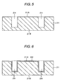
- Fig. 1 is a sectional diagram of a related-art substrate with through electrodes.
- the related-art substrate 200 with the through electrodes has a substrate 201, an insulating film 202 and through electrodes 203.
- the substrate 201 is formed in a plate shape, and through holes 205 are formed in the substrate 201.
- a silicon substrate can be used as the substrate 201.
- the insulating film 202 is disposed so as to cover an upper surface 201A of the substrate 201 and a surface of the substrate 201 of the portion exposed to the through holes 205.
- an oxide film formed by a CVD method can be used as the insulating film 202.
- the through electrode 203 is disposed in the through hole 205 on which the insulating film 202 is formed.
- the through electrode 203 has a seed layer 207 and a Cu plated film 208.
- the seed layer 207 is disposed so as to cover the insulating film 202 formed on the through hole 205.
- the seed layer 207 is a power feeding layer for forming the Cu plated film 208 by an electrolytic plating method.
- As the seed layer 207 for example, a Cu layer formed by a metal CVD method can be used.
- the Cu plated film 208 is disposed so as to fill the through hole 205 on which the insulating film 202 and the seed layer 207 are formed.
- One end of the through electrode 203 constructed as described above is connected to a semiconductor chip (not shown) and the other end is connected to a mounting substrate (not shown) such as a motherboard.
- Figs. 2 to 12 are diagrams showing manufacturing steps of the related-art substrate with the through electrodes.
- the same numerals are assigned to the same components as those of the related-art substrate 200 with the through electrodes.
- a substrate 211 used as a base material of the substrate 201 described previously is prepared.
- a substrate with a thickness thicker than that of the substrate 201 is used.
- a silicon substrate can be used as the substrate 211.
- a resist film 212 having opening parts 212A is formed on an upper surface 211A of the substrate 211.
- the opening part 212A is formed so as to expose the upper surface 211A of the substrate 211 of the portion corresponding to a formation region of the through hole 205.
- opening parts 214 are formed in the substrate 211 by anisotropic etching using the resist film 212 as a mask.
- the opening part 214 results in a through hole 205 by polishing the substrate 211 in a step shown in Fig. 11 described below. Therefore, the opening part 214 is formed so that the depth becomes deeper than a depth of the through hole 205.
- the resist film 212 shown in Fig. 4 is removed.
- an insulating film 202 is formed so as to cover the upper surface 211A of the substrate 211 and a surface of the substrate 211 of the portion in which the opening parts 214 are formed by a CVD method.
- the insulating film 202 for example, an oxide film can be used.
- a seed layer 207 is formed so as to cover the insulating film 202 by a metal CVD method.
- a seed layer 207 for example, a Cu layer can be used.
- a Cu plated film 208 is formed on the seed layer 207 by an electrolytic plating method using the seed layer 207 as a power feeding layer.
- the Cu plated film 208 is formed so as to fill the opening parts 214 on which the insulating film 202 and the seed layer 207 are formed.
- the Cu plated film 208 grows in a direction from the seed layer 207 formed on side surfaces of the opening parts 214 toward the centers of the opening parts 214.
- the extra Cu plated film 208 is polished by a CMP apparatus. This polishing is performed until the insulating film 202 formed on the upper surface 211A of the substrate 211 is exposed. Then, in a step shown in Fig. 10 , a support plate 217 is stuck on the upper surface side of a structural body shown in Fig. 9 by an adhesive 216.
- the substrate 211, the insulating film 202, the seed layer 207 and the Cu plated film 208 are polished from the side of a lower surface 211B of the substrate 211 shown in Fig. 10 using a back polishing apparatus, and a substrate 201 having through holes 205 and through electrodes 203 formed in the through holes 205 through the insulating film 202 are formed. Consequently, a structural body corresponding to a substrate 200 with through electrodes is formed under the support plate 217.
- the CMP apparatus with high processing cost is used, so that there was a problem that a manufacturing cost of the substrate 200 with the through electrodes increases.
- the substrate 211, the insulating film 202, the seed layer 207 and the Cu plated film 208 are polished using the back polishing apparatus, so that there was a problem that a crack occurs in the through electrode 203 and the through electrode 203 breaks.
- the Cu plated film 208 which is one of the components of the through electrode 203 is grown in the direction from the seed layer 207 formed on the side surfaces of the opening parts 214 toward the centers of the opening parts 214, so that there was a problem that a void tends to occur in the center of the through electrode 203.
- Exemplary embodiments of the present invention provide a manufacturing method of a substrate with a through electrode capable of preventing breakage of the through electrode and reducing a manufacturing cost of the substrate with the through electrode and also preventing occurrence of a void in the through electrode.
- a manufacturing method of a substrate with a through electrode includes a through electrode formation step of forming a through electrode on a support plate, a substrate formation step of forming a substrate having a through hole, a through electrode reception step of stacking the substrate on the support plate and receiving the through electrode in the through hole, a resin filling step of filling a gap between a side surface of the through electrode and an inner wall of the through hole of the substrate with a resin, and a support plate removal step of removing the support plate after the resin filling step.
- a substrate with a through electrode is manufactured. Therefore, the need for polishing using a CMP apparatus with high processing cost or a back polishing apparatus required in related art is eliminated, so that breakage of the through electrode can be prevented and also a manufacturing cost of the substrate with the through electrode can be reduced.
- the through electrode formation step it may be constructed so that a resist film having an opening part is formed on the support plate and thereafter, a plated film is precipitated from the top of the support plate exposed to a bottom part of the opening part toward the opening end of the opening part by electrolytic plating and the through electrode is formed and after the through electrode is formed, the resist film is removed.
- a void By precipitating the plated film from the top of the support plate exposed to the bottom part of the opening part toward the opening end of the opening part thus, a void can be prevented from occurring in the through electrode.
- breakage of a through electrode can be prevented and a manufacturing cost of a substrate with the through electrode can be reduced and also occurrence of a void in the through electrode can be prevented.
- a manufacturing method of a substrate with through electrodes comprising a substrate having through holes, and through electrodes received in the through holes, is provided.
- the method includes a through electrode formation step of forming the through electrodes on a support plate, a substrate formation step of forming the substrate, a through electrode reception step of stacking the substrate on the support plate and receiving the through electrodes in the through holes, a resin filling step of filling gaps between side surfaces of the through electrodes and inner walls of the through holes of the substrate with a resin, and a support plate removal step of removing the support plate after the resin filling step.
- a substrate with through electrodes having a substrate, a resin, and a through electrode, wherein the substrate has a through hole, and the resin is disposed so as to fill a gap formed between a side surface of the through electrode and an inner wall of the through hole.
- the substrate may include a wiring layer, which is electrically connected to the through electrode, on a surface of the substrate.
- Fig. 13 is a sectional diagram of a substrate with through electrodes according to a first embodiment of the invention.
- a substrate 10 with through electrodes of the present embodiment has a substrate 11, a resin 12, a diffusion preventive film 13, through electrodes 14, a build-up structural body 16 which is a wiring layer, and external connection terminals 17.
- the substrate 11 is formed in a plate shape, and has plural through holes 18.
- a diameter R1 of the through hole 18 can be set at a value larger than a diameter R2 of the through electrode 14 by, for example, 20 ⁇ m or more.
- the substrate 11 for example, a silicon substrate or a quartz glass substrate can be used.
- a thickness M1 of the substrate 11 is set so as to become substantially equal to a value in which a length L1 of the through electrode 14 and a thickness of the diffusion preventive film 13 are added. In the embodiment, the following description will be made by taking the case of using a silicon substrate as the substrate 11 as an example.
- the resin 12 is disposed so as to fill a gap formed between side surfaces of the through electrodes 14 and the diffusion preventive film 13 and the substrate 11 (in other words, inner walls of the through holes 18) of the portion opposed to the side surfaces of the through electrodes 14 and the diffusion preventive film 13.
- the resin 12 is means for insulating the substrate 11 from the diffusion preventive film 13 and the through electrodes 14.
- an epoxy resin can be used as the resin 12, for example.
- the diffusion preventive film 13 is configured to have an Au layer 21 and a Ni layer 22 laminated on the Au layer 21.
- the diffusion preventive film 13 is disposed in the plural through holes 18 so that a lower surface of the Au layer 21 is substantially flush with a lower surface 11B of the substrate 11.
- a thickness of the Au layer 21 can be set at, for example, 0.1 ⁇ m.
- a thickness of the Ni layer 22 can be set at, for example, 2 ⁇ m.
- the diffusion preventive film 13 is a film for preventing Cu included in the through electrode 14 from diffusing into the external connection terminal 17.
- the through electrode 14 is disposed in the through hole 18 through the resin 12.
- the lower end of the through electrode 14 is in contact with the Ni layer 22. Consequently, the through electrode 14 is electrically connected to the diffusion preventive film 13.
- An upper surface 14A of the through electrode 14 is made substantially flush with an upper surface 11A of the substrate 11.
- the diameter R2 of the through electrode 14 can be set at, for example, 20 ⁇ m to 150 ⁇ m.
- the length L1 of the through electrode 14 can be set at, for example, 50 ⁇ m to 300 ⁇ m.
- the build-up structural body 16 has resin layers 25, 28, wiring patterns 26, 29, a solder resist 32, and a diffusion preventive film 33.
- the resin layer 25 is disposed so as to cover a part of the upper surface 14A of the through electrode 14, an upper surface of the resin 12 and the upper surface 11A of the substrate 11.
- the resin layer 25 has an opening part 35 for exposing a part of the upper surface 14A of the through electrode 14.
- an epoxy resin can be used as a material of the resin layer 25, for example.
- the wiring pattern 26 is disposed on an upper surface 25A of the resin layer 25 and the opening part 35 so as to electrically connect the two adjacent through electrodes 14 as one example.
- a material of the wiring pattern 26, for example, Cu can be used.
- the resin layer 28 is disposed so as to cover a part of the wiring pattern 26 and an upper surface 25A of the resin layer 25.
- the resin layer 28 has an opening part 37 for exposing an upper surface of the wiring pattern 26 of the portion arranged on the upper surface 25A of the resin layer 25.
- an epoxy resin can be used as a material of the resin layer 28, for example.
- the wiring pattern 29 is disposed so as to extend from the opening part 37 to an upper surface 28A of the resin layer 28 while filling the opening part 37.
- the wiring pattern 29 is electrically connected to the wiring pattern 26.
- the wiring pattern 29 has a diffusion preventive film formation region in which the diffusion preventive film 33 is formed.
- the solder resist 32 is disposed so as to cover the upper surface 28A of the resin layer 28 and a part of the wiring pattern 29.
- the solder resist 32 has an opening part 32A for exposing the diffusion preventive film formation region of the wiring pattern 29.
- the diffusion preventive film 33 is disposed on the wiring pattern 29 of the portion exposed to the opening part 32A.
- the diffusion preventive film 33 is configured to sequentially laminate a Ni layer 38 and an Au layer 39 on the wiring pattern 29.
- a thickness of the Ni layer 38 can be set at, for example, 2 ⁇ m.
- a thickness of the Au layer 39 can be set at, for example, 0.1 ⁇ m.
- An electronic component (for example, a semiconductor chip) is mounted on the diffusion preventive film 33.
- the diffusion preventive film 33 is a pad for installing the electronic component.
- a range of selection of an electronic component installation position can be widened by adjusting routing of the wiring pattern 29 and disposing the diffusion preventive film 33 in any position.
- the external connection terminal 17 is disposed on the side of a lower surface 21A of the Au layer 21.
- the external connection terminal 17 is electrically connected to the through electrode 14 through the diffusion preventive film 13.
- the external connection terminal 17 is a terminal connected to a mounting substrate (not shown) such as a motherboard.
- a solder bump can be used as the external connection terminal 17, for example.
- Figs. 14 to 29 are diagrams showing manufacturing steps of the substrate with the through electrodes according to the first embodiment of the invention.
- the same numerals are assigned to the same components as those of the substrate 10 with the through electrodes of the first embodiment.
- a support plate 45 formed in a plate shape is prepared.
- a silicon substrate or a metal plate for example, a Cu plate
- the following description will be made by taking the case of using the silicon substrate as the support plate 45 as an example.
- a thickness M2 of the support plate 45 can be set at, for example, 0.4 mm to 0.8 mm.
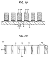
- a seed layer 46 is formed so as to cover an upper surface 45A of the support plate 45.
- a Cu layer can be used as the seed layer 46.
- the Cu layer can be formed by, for example, a sputtering method.
- the metal plate functions as a seed layer, so that the need for formation of the seed layer 46 is eliminated.
- a resist film 48 having plural opening parts 48A is formed on the seed layer 46.
- a diameter of the opening part 48A is formed so as to become substantially equal to the diameter R2 (see Fig. 13 ) of the through electrode 14 described above. Also, the opening part 48A is formed so as to expose an upper surface of the seed layer 46.
- a diffusion preventive film 13 is formed by sequentially precipitating and growing an Au layer 21 and a Ni layer 22 on the seed layer 46 of the portion exposed to the opening part 48A by an electrolytic plating method using the seed layer 46 as a power feeding layer.
- a through electrode 14 made of a plated film is formed by precipitating and growing the plated film on the Ni layer 22 by an electrolytic plating method using the seed layer 46 as a power feeding layer (a through electrode formation step). At this time, the plated film is precipitated and grown from the top of the Ni layer 22 toward the opening end of the opening part 48A (the upper end of the opening part 48A).
- the through electrode 14 can be formed without polishing a base material (the seed layer 207 and the Cu plated film 208) resulting in the through electrode 203 by a CMP apparatus with high processing cost (see Fig. 9 ) or polishing a base material (the seed layer 207 and the Cu plated film 208) resulting in the through electrode 203 and the substrate 211 by a back polishing apparatus (see Fig. 11 ) as described in the manufacturing method of the related-art substrate 200 with the through electrodes. Therefore, breakage of the through electrode 14 can be prevented and also a manufacturing cost of the substrate 10 with the through electrodes can be reduced.
- the diameter R2 of the through electrode 14 can be set at, for example, 20 ⁇ m to 150 ⁇ m. Also, the length L1 of the through electrode 14 can be set at, for example, 50 ⁇ m to 300 ⁇ m.
- a substrate 11 having plural through holes 18 is formed (a substrate formation step).
- the plural through holes 18 can be formed by, for example, anisotropic etching of the substrate 11.
- the through hole 18 is formed so that its diameter R1 becomes larger than the diameter R2 of the through electrode 14 by, for example, 20 ⁇ m or more.
- the substrate 11 for example, a silicon substrate or a quartz glass substrate can be used. In the embodiment, the silicon substrate is taken as an example.
- the thickness M1 of the substrate 11 is set so as to become substantially equal to a value in which the length L1 of the through electrode 14 and the thickness of the diffusion preventive film 13 are added. Consequently, in a step shown in Fig. 21 described below, an upper surface 14A of the through electrode 14 can be made substantially flush with an upper surface 11A of the substrate 11. In addition, the upper surface 14A of the through electrode 14 may be somewhat protruded or recessed from the upper surface 11A of the substrate 11.
- the substrate 11 shown in Fig. 20 is stacked on a structural body shown in Fig. 19 and the through electrodes 14 are received in the through holes 18 of the substrate 11 so that gaps can be formed between the substrate 11 and the through electrodes 14 (gaps can be formed between inner walls of the through holes 18 and side surfaces of the through electrodes 14) (a through electrode reception step) .
- the substrate 11 and the structural body shown in Fig. 19 are temporarily fixed by some jig such as a clip so that a relative position of the substrate 11 with respect to the structural body shown in Fig. 19 is not displaced.
- a resin 12 is formed so as to fill the gaps between the inner walls of the through holes 18 and the side surfaces of the through electrodes 14 and also cover an upper surface of a structural body shown in Fig. 21 (a resin filling step).
- the resin 12 is formed by, for example, softening an epoxy resin after a filmy epoxy resin is stuck so as to cover the upper surface of the structural body shown in Fig. 21 .
- the resin 12 is formed by, for example, applying a liquid epoxy resin by a print method and thereafter curing the epoxy resin.
- the resin 12 of the portion for covering the upper surface of the structural body shown in Fig. 21 among the resin 12 formed in the step shown in Fig. 22 results in a base material of a resin layer 25 (see Fig. 13 ) which is one of the components of the build-up structural body 16 described above by forming opening parts 35 in a step shown in Fig. 23 described below.
- the manufacturing steps of the substrate 10 with the through electrodes can be simplified. Also, it serves as a substitute for an oxide film (insulating film) by a related-art CVDmethod, and cost reduction and simplification of the steps can be achieved.
- the opening parts 35 for exposing a part of the upper surfaces 14A of the through electrodes 14 are formed in the resin 12 (see Fig. 22 ) of the portion for covering the upper surface of the structural body shown in Fig. 21 . Consequently, the resin layer 25 having the plural opening parts 35 is formed.
- the opening parts 35 can be formed by, for example, laser machining.
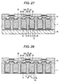
- a wiring pattern 26 for electrically connecting the two adjacent through electrodes 14 is formed on the upper surface side of a structural body shown in Fig. 23 .
- the wiring pattern 26 can be formed by, for example, a semi-additive method.
- a Cu plated film can be used as the wiring pattern 26.
- a resin layer 28 having opening parts 37 for exposing a part of the wiring pattern 26 and a wiring pattern 29 arranged so as to fill the opening parts 37 and also extend from the opening parts 37 to an upper surface 28A of the resin layer 28 are sequentially formed on a structural body shown in Fig. 24 by a well-known technique such as a semi-additive method.
- a resin layer 28 for example, an epoxy resin can be used.
- a solder resist 32 having opening parts 32A for exposing a part of an upper surface of the wiring pattern 29 is formed on the resin layer 28.
- a diffusion preventive film 33 is formed by sequentially precipitating and growing a Ni layer 38 and an Au layer 39 on the wiring pattern 29 of the portion exposed to the opening part 32A by an electrolytic plating method using the seed layer 46 as a power feeding layer. Consequently, the build-up structural body 16 is formed.
- the steps shown in Figs. 22 to 27 are a step corresponding to a build-up structural body formation step.
- the build-up structural body 16 By forming the build-up structural body 16 on the substrate 11 in which the through electrodes 14 are formed thus, a range of selection of an electronic component installation position can be widened by adjusting routing of the wiring pattern 29 and disposing the diffusion preventive film 33 in any position.
- the Ni layer 38 and the Au layer 39 may be formed using an electroless plating method.
- the support plate 45 and the seed layer 46 are sequentially removed. Concretely, for example, the support plate 45 and the seed layer 46 are removed by etching.
- external connection terminals 17 are formed on the sides of lower surfaces 21A of the Au layers 21. Consequently, the substrate 10 with the through electrodes is manufactured.
- a solder bump can be used as the external connection terminal 17, for example.
- the through electrodes 14 can be formed without polishing a base material (the seed layer 207 and the Cu plated film 208) resulting in the through electrode 203 by a CMP apparatus (see Fig.
- the through electrodes 14 are formed by the semi-additive method, so that a void can be prevented from occurring in the through electrode 14.
- an element for example, a passive element, an active element or a semiconductor circuit
- an element electrically connected to the through electrodes 14 may be disposed on the substrate 11 and also in the substrate with the through electrodes constructed thus, an effect similar to that of the manufacturing method of the substrate 10 with the through electrodes of the embodiment can be obtained.
- the manufacturing steps described above are performed and thereafter the support plate and the substrate are cut and thereby, the plural substrates 10 with the through electrodes may be manufactured.
- Fig. 30 is a sectional diagram of a substrate with through electrodes according to a second embodiment of the invention.
- the same numerals are assigned to the same components as those of the substrate 10 with the through electrodes of the first embodiment.
- a substrate 60 with through electrodes of the second embodiment is constructed in a manner similar to the substrate 10 with the through electrodes except that a diffusion preventive film 33 is disposed on through electrodes 14 exposed to opening parts 35 formed in a resin layer 25 while the resin layer 28, the wiring patterns 26, 29 and the solder resist 32 are excluded from the components of the substrate 10 with the through electrodes of the first embodiment.
- the substrate 60 with the through electrodes of the second embodiment constructed as described above can be manufactured by forming the diffusion preventive film 33 on upper surfaces 14A of the through electrodes 14 after the step shown in Fig. 23 described in the first embodiment and then removing a support plate 45 and a seed layer 46.
- a manufacturing method of the substrate with the through electrodes of the embodiment can obtain an effect similar to that of the manufacturing method of the substrate 10 with the through electrodes of the first embodiment.
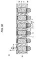
- Fig. 31 is a sectional diagram of a substrate with through electrodes according to a third embodiment of the invention.
- the same numerals are assigned to the same components as those of the substrate 10 with the through electrodes of the first embodiment.
- a substrate 70 with through electrodes of the third embodiment is constructed in a manner similar to the substrate 10 with the through electrodes except that a conductor layer 71 is further disposed while disposing a build-up structural body 72 instead of the build-up structural body 16 disposed in the substrate 10 with the through electrodes of the first embodiment.
- the conductor layer 71 is disposed so as to cover inner walls of through holes 18 and an upper surface 11A and a lower surface 11B of a substrate 11. By disposing the conductor layer 71 on the inner walls of the through holes 18, through electrodes 14 can be formed in a coaxial structure.
- the conductor layer 71 is a layer acting as a power source potential or a ground potential by being connected to a wiring pattern 73 described below.
- the conductor layer 71 can be constructed by, for example, a Cu plated film formed by an electroless plating method and a Cu plated film formed by an electrolytic plating method.
- the build-up structural body 72 is disposed on the substrate 11 in which the conductor layer 71 is formed.
- the build-up structural body 72 has construction similar to the build-up structural body 16 except that the wiring pattern 73 is further disposed in the construction of the build-up structural body 16 described in the first embodiment.
- the wiring pattern 73 is disposed on the conductor layer 71 formed on the upper surface 11A of the substrate 11 and opening parts 35 so as to electrically connect the two adjacent through electrodes 14 to the conductor layer 71 as one example.
- As a material of the wiring pattern 73 for example, Cu can be used.
- the substrate 70 with the through electrodes of the third embodiment constructed as described above can be manufactured by a technique similar to that of the substrate 10 with the through electrodes of the first embodiment, and can obtain an effect similar to that of the manufacturing method of the substrate 10 with the through electrodes of the first embodiment.
- the invention can be applied to a manufacturing method of a substrate with a through electrode comprising a through electrode extending through a substrate. While the invention has been described with respect to a limited number of embodiments, those skilled in the art, having benefit of this disclosure, will appreciate that other embodiments canbe devised which do not depart from the scope of the invention as disclosed herein. Accordingly, the scope of the invention should be limited only by the attached claims.
- This application claims priority to Japanese Patent Application No. 2007-148182, filed June 4, 2007 , in the Japanese Patent Office.
- the Japanese Patent Application No. 2007-148182 is incorporated by reference in its entirety.
Landscapes
- Engineering & Computer Science (AREA)
- Manufacturing & Machinery (AREA)
- Microelectronics & Electronic Packaging (AREA)
- Chemical & Material Sciences (AREA)
- Inorganic Chemistry (AREA)
- Internal Circuitry In Semiconductor Integrated Circuit Devices (AREA)
- Printing Elements For Providing Electric Connections Between Printed Circuits (AREA)
- Electrostatic, Electromagnetic, Magneto- Strictive, And Variable-Resistance Transducers (AREA)
- Pressure Sensors (AREA)
- Printers Or Recording Devices Using Electromagnetic And Radiation Means (AREA)
Applications Claiming Priority (1)
| Application Number | Priority Date | Filing Date | Title |
|---|---|---|---|
| JP2007148182A JP5193503B2 (ja) | 2007-06-04 | 2007-06-04 | 貫通電極付き基板及びその製造方法 |
Publications (2)
| Publication Number | Publication Date |
|---|---|
| EP2001274A2 true EP2001274A2 (fr) | 2008-12-10 |
| EP2001274A3 EP2001274A3 (fr) | 2009-11-11 |
Family
ID=39731510
Family Applications (1)
| Application Number | Title | Priority Date | Filing Date |
|---|---|---|---|
| EP08157592A Withdrawn EP2001274A3 (fr) | 2007-06-04 | 2008-06-04 | Procédé de fabrication d'un substrat avec électrodes traversantes |
Country Status (6)
| Country | Link |
|---|---|
| US (1) | US8349733B2 (fr) |
| EP (1) | EP2001274A3 (fr) |
| JP (1) | JP5193503B2 (fr) |
| KR (1) | KR20080106844A (fr) |
| CN (1) | CN101320695A (fr) |
| TW (1) | TW200850096A (fr) |
Cited By (1)
| Publication number | Priority date | Publication date | Assignee | Title |
|---|---|---|---|---|
| WO2012096765A1 (fr) * | 2011-01-14 | 2012-07-19 | Harris Corporation | Procédé de fabrication d'un dispositif électronique comportant un masque de soudure polymère à cristaux liquides stratifié sur un empilage de couches d'interconnexion, et dispositifs associés |
Families Citing this family (20)
| Publication number | Priority date | Publication date | Assignee | Title |
|---|---|---|---|---|
| US8288872B2 (en) * | 2008-08-05 | 2012-10-16 | Taiwan Semiconductor Manufacturing Company, Ltd. | Through silicon via layout |
| US8294240B2 (en) * | 2009-06-08 | 2012-10-23 | Qualcomm Incorporated | Through silicon via with embedded decoupling capacitor |
| KR101095373B1 (ko) * | 2010-04-22 | 2011-12-16 | 재단법인 서울테크노파크 | 장벽층을 갖는 범프를 포함하는 반도체칩 및 그 제조방법 |
| JP5547566B2 (ja) * | 2010-06-29 | 2014-07-16 | 株式会社アドバンテスト | 貫通配線基板の製造方法 |
| JP5485818B2 (ja) * | 2010-06-29 | 2014-05-07 | 株式会社アドバンテスト | 貫通配線基板および製造方法 |
| KR20120012602A (ko) * | 2010-08-02 | 2012-02-10 | 삼성전자주식회사 | 반도체 장치, 그 제조 방법 및 반도체 패키지의 제조 방법 |
| US8472207B2 (en) * | 2011-01-14 | 2013-06-25 | Harris Corporation | Electronic device having liquid crystal polymer solder mask and outer sealing layers, and associated methods |
| JP2012156327A (ja) | 2011-01-26 | 2012-08-16 | Elpida Memory Inc | 半導体装置、及び積層型半導体装置 |
| KR101806806B1 (ko) | 2011-12-20 | 2017-12-11 | 삼성전자주식회사 | 전자 소자 탑재용 기판의 제조방법 |
| JP5878362B2 (ja) * | 2011-12-22 | 2016-03-08 | 新光電気工業株式会社 | 半導体装置、半導体パッケージ及び半導体装置の製造方法 |
| TWI475623B (zh) * | 2011-12-27 | 2015-03-01 | 財團法人工業技術研究院 | 堆疊式半導體結構的接合結構及其形成方法 |
| CN104051369A (zh) * | 2014-07-02 | 2014-09-17 | 上海朕芯微电子科技有限公司 | 一种用于2.5d封装的中间互联层及其制备方法 |
| JP2016039512A (ja) | 2014-08-08 | 2016-03-22 | キヤノン株式会社 | 電極が貫通配線と繋がったデバイス、及びその製造方法 |
| US10431533B2 (en) * | 2014-10-31 | 2019-10-01 | Ati Technologies Ulc | Circuit board with constrained solder interconnect pads |
| KR102494336B1 (ko) * | 2015-10-07 | 2023-02-01 | 삼성전기주식회사 | 인쇄회로기판 및 그 제조방법 |
| JP6424297B2 (ja) * | 2016-03-25 | 2018-11-14 | 住友精密工業株式会社 | 充填方法 |
| US20190140167A1 (en) * | 2017-11-07 | 2019-05-09 | Everspin Technologies, Inc. | Angled surface removal process and structure relating thereto |
| CN108122835B (zh) * | 2017-12-12 | 2020-11-20 | 华进半导体封装先导技术研发中心有限公司 | 转接板的制造方法及其所制造的转接板 |
| WO2022158109A1 (fr) * | 2021-01-19 | 2022-07-28 | ソニーセミコンダクタソリューションズ株式会社 | Dispositif à semi-conducteur et procédé de fabrication de dispositif à semi-conducteur |
| CN113021172A (zh) * | 2021-03-25 | 2021-06-25 | 中国电子科技集团公司第五十四研究所 | 一种带腔ltcc基板的研磨抛光方法 |
Citations (5)
| Publication number | Priority date | Publication date | Assignee | Title |
|---|---|---|---|---|
| US5485039A (en) * | 1991-12-27 | 1996-01-16 | Hitachi, Ltd. | Semiconductor substrate having wiring conductors at a first main surface electrically connected to plural pins at a second main surface |
| JP2004221240A (ja) | 2003-01-14 | 2004-08-05 | Mitsubishi Electric Corp | 半導体装置の製造方法 |
| US20040259351A1 (en) * | 2003-06-19 | 2004-12-23 | Naoyuki Koizumi | Method for manufacturing semiconductor package |
| EP1746652A1 (fr) * | 2005-07-19 | 2007-01-24 | Shinko Electric Industries Co., Ltd. | Substrat de circuit et son procédé de fabrication |
| JP2007148182A (ja) | 2005-11-30 | 2007-06-14 | Ricoh Co Ltd | 現像装置及び画像形成装置 |
Family Cites Families (18)
| Publication number | Priority date | Publication date | Assignee | Title |
|---|---|---|---|---|
| WO2001026147A1 (fr) * | 1999-10-04 | 2001-04-12 | Seiko Epson Corporation | Dispositif a semi-conducteur, son procede de fabrication, carte de circuit imprime et dispositif electronique |
| JP4023076B2 (ja) * | 2000-07-27 | 2007-12-19 | 富士通株式会社 | 表裏導通基板及びその製造方法 |
| JP2002314244A (ja) * | 2001-04-11 | 2002-10-25 | Ngk Insulators Ltd | コア基板とその製造方法、該コア基板を用いた複層コア基板の製造方法及び多層積層基板の製造方法 |
| KR100435813B1 (ko) * | 2001-12-06 | 2004-06-12 | 삼성전자주식회사 | 금속 바를 이용하는 멀티 칩 패키지와 그 제조 방법 |
| JP4045143B2 (ja) * | 2002-02-18 | 2008-02-13 | テセラ・インターコネクト・マテリアルズ,インコーポレイテッド | 配線膜間接続用部材の製造方法及び多層配線基板の製造方法 |
| JP2005026313A (ja) * | 2003-06-30 | 2005-01-27 | Shinko Electric Ind Co Ltd | 配線基板の製造方法 |
| JP3938921B2 (ja) * | 2003-07-30 | 2007-06-27 | Tdk株式会社 | 半導体ic内蔵モジュールの製造方法 |
| US7547975B2 (en) * | 2003-07-30 | 2009-06-16 | Tdk Corporation | Module with embedded semiconductor IC and method of fabricating the module |
| JP2005072064A (ja) * | 2003-08-27 | 2005-03-17 | Ngk Spark Plug Co Ltd | 配線基板およびその製造方法 |
| JP2005072061A (ja) * | 2003-08-27 | 2005-03-17 | Ngk Spark Plug Co Ltd | 配線基板およびその製造方法 |
| JP4438389B2 (ja) * | 2003-11-14 | 2010-03-24 | カシオ計算機株式会社 | 半導体装置の製造方法 |
| JP3751625B2 (ja) * | 2004-06-29 | 2006-03-01 | 新光電気工業株式会社 | 貫通電極の製造方法 |
| JP4813035B2 (ja) * | 2004-10-01 | 2011-11-09 | 新光電気工業株式会社 | 貫通電極付基板の製造方法 |
| JP3987521B2 (ja) * | 2004-11-08 | 2007-10-10 | 新光電気工業株式会社 | 基板の製造方法 |
| JP2006147873A (ja) * | 2004-11-19 | 2006-06-08 | Sharp Corp | 半導体装置の製造方法 |
| JP2006165112A (ja) * | 2004-12-03 | 2006-06-22 | Sharp Corp | 貫通電極形成方法およびそれを用いる半導体装置の製造方法、ならびに該方法によって得られる半導体装置 |
| US7863189B2 (en) * | 2007-01-05 | 2011-01-04 | International Business Machines Corporation | Methods for fabricating silicon carriers with conductive through-vias with low stress and low defect density |
| JP5302522B2 (ja) * | 2007-07-02 | 2013-10-02 | スパンション エルエルシー | 半導体装置及びその製造方法 |
-
2007
- 2007-06-04 JP JP2007148182A patent/JP5193503B2/ja active Active
-
2008
- 2008-06-02 KR KR1020080051603A patent/KR20080106844A/ko not_active Withdrawn
- 2008-06-03 US US12/132,187 patent/US8349733B2/en active Active
- 2008-06-03 TW TW097120562A patent/TW200850096A/zh unknown
- 2008-06-04 CN CNA2008101086822A patent/CN101320695A/zh active Pending
- 2008-06-04 EP EP08157592A patent/EP2001274A3/fr not_active Withdrawn
Patent Citations (5)
| Publication number | Priority date | Publication date | Assignee | Title |
|---|---|---|---|---|
| US5485039A (en) * | 1991-12-27 | 1996-01-16 | Hitachi, Ltd. | Semiconductor substrate having wiring conductors at a first main surface electrically connected to plural pins at a second main surface |
| JP2004221240A (ja) | 2003-01-14 | 2004-08-05 | Mitsubishi Electric Corp | 半導体装置の製造方法 |
| US20040259351A1 (en) * | 2003-06-19 | 2004-12-23 | Naoyuki Koizumi | Method for manufacturing semiconductor package |
| EP1746652A1 (fr) * | 2005-07-19 | 2007-01-24 | Shinko Electric Industries Co., Ltd. | Substrat de circuit et son procédé de fabrication |
| JP2007148182A (ja) | 2005-11-30 | 2007-06-14 | Ricoh Co Ltd | 現像装置及び画像形成装置 |
Cited By (4)
| Publication number | Priority date | Publication date | Assignee | Title |
|---|---|---|---|---|
| WO2012096765A1 (fr) * | 2011-01-14 | 2012-07-19 | Harris Corporation | Procédé de fabrication d'un dispositif électronique comportant un masque de soudure polymère à cristaux liquides stratifié sur un empilage de couches d'interconnexion, et dispositifs associés |
| US8693203B2 (en) | 2011-01-14 | 2014-04-08 | Harris Corporation | Method of making an electronic device having a liquid crystal polymer solder mask laminated to an interconnect layer stack and related devices |
| TWI471957B (zh) * | 2011-01-14 | 2015-02-01 | 賀利實公司 | 製造具有層疊至一互連層堆疊之一液晶聚合物焊料光罩之一電子裝置之方法及其相關裝置 |
| US9059317B2 (en) | 2011-01-14 | 2015-06-16 | Harris Corporation | Method of making an electronic device having a liquid crystal polymer solder mask laminated to an interconnect layer stack and related devices |
Also Published As
| Publication number | Publication date |
|---|---|
| US20080299768A1 (en) | 2008-12-04 |
| US8349733B2 (en) | 2013-01-08 |
| TW200850096A (en) | 2008-12-16 |
| KR20080106844A (ko) | 2008-12-09 |
| CN101320695A (zh) | 2008-12-10 |
| EP2001274A3 (fr) | 2009-11-11 |
| JP2008300782A (ja) | 2008-12-11 |
| JP5193503B2 (ja) | 2013-05-08 |
Similar Documents
| Publication | Publication Date | Title |
|---|---|---|
| EP2001274A2 (fr) | Procédé de fabrication d'un substrat avec électrodes traversantes | |
| CN1855451B (zh) | 半导体装置及其制造方法 | |
| US7772118B2 (en) | Substrate having high electrical connection reliability of a penetrating via connected to wirings and a method for manufacturing the same | |
| US7932471B2 (en) | Capacitor for incorporation in wiring board, wiring board, method of manufacturing wiring board, and ceramic chip for embedment | |
| US8324513B2 (en) | Wiring substrate and semiconductor apparatus including the wiring substrate | |
| US8344492B2 (en) | Semiconductor device and method of manufacturing the same, and electronic apparatus | |
| KR101392950B1 (ko) | 배선기판 및 배선기판 제조방법 | |
| US8759685B2 (en) | Wiring substrate and method of manufacturing the wiring substrate | |
| EP2009692A1 (fr) | Module électronique et son procédé de fabrication | |
| EP1489658B1 (fr) | Méthode de formation pour boîtier à semi-conducteur | |
| US8330050B2 (en) | Wiring board having heat intercepting member | |
| KR20080099192A (ko) | 빌트-인 부품을 갖는 와이어링 보드 및 그의 제조방법 | |
| CN100501986C (zh) | 半导体装置及其制造方法 | |
| US20160293535A1 (en) | Wiring substrate and semiconductor package | |
| US11183483B2 (en) | Multichip module and electronic device | |
| US20200279801A1 (en) | Foil-based package with distance compensation | |
| US8110921B2 (en) | Semiconductor package and method of manufacturing the same | |
| KR20060053087A (ko) | 기판, 반도체 장치, 기판 제조 방법, 및 반도체 장치 제조방법 | |
| US7772109B2 (en) | Manufacturing method of multilayer wiring substrate | |
| CN100552926C (zh) | 半导体器件、配线基板及其制造方法 | |
| CN104701187A (zh) | 半导体装置以及其制备方法 | |
| CN102099281A (zh) | 用于制造构件的方法、用于制造构件结构的方法、构件和构件结构 | |
| CN1873935B (zh) | 配线基板的制造方法及半导体器件的制造方法 | |
| KR20080085682A (ko) | 전자 장치의 제조 방법, 기판 및 반도체 장치 | |
| EP2006911B1 (fr) | Substrat de câblage |
Legal Events
| Date | Code | Title | Description |
|---|---|---|---|
| PUAI | Public reference made under article 153(3) epc to a published international application that has entered the european phase |
Free format text: ORIGINAL CODE: 0009012 |
|
| AK | Designated contracting states |
Kind code of ref document: A2 Designated state(s): AT BE BG CH CY CZ DE DK EE ES FI FR GB GR HR HU IE IS IT LI LT LU LV MC MT NL NO PL PT RO SE SI SK TR |
|
| AX | Request for extension of the european patent |
Extension state: AL BA MK RS |
|
| PUAL | Search report despatched |
Free format text: ORIGINAL CODE: 0009013 |
|
| AK | Designated contracting states |
Kind code of ref document: A3 Designated state(s): AT BE BG CH CY CZ DE DK EE ES FI FR GB GR HR HU IE IS IT LI LT LU LV MC MT NL NO PL PT RO SE SI SK TR |
|
| AX | Request for extension of the european patent |
Extension state: AL BA MK RS |
|
| 17P | Request for examination filed |
Effective date: 20100511 |
|
| AKX | Designation fees paid |
Designated state(s): DE |
|
| 17Q | First examination report despatched |
Effective date: 20100915 |
|
| STAA | Information on the status of an ep patent application or granted ep patent |
Free format text: STATUS: THE APPLICATION HAS BEEN WITHDRAWN |
|
| 18W | Application withdrawn |
Effective date: 20150318 |