EP2003430A2 - Verfahren zur Herstellung eines Ultraschallsensors - Google Patents
Verfahren zur Herstellung eines Ultraschallsensors Download PDFInfo
- Publication number
- EP2003430A2 EP2003430A2 EP20080251485 EP08251485A EP2003430A2 EP 2003430 A2 EP2003430 A2 EP 2003430A2 EP 20080251485 EP20080251485 EP 20080251485 EP 08251485 A EP08251485 A EP 08251485A EP 2003430 A2 EP2003430 A2 EP 2003430A2
- Authority
- EP
- European Patent Office
- Prior art keywords
- conductive
- case
- piezoelectric element
- ultrasonic sensor
- conductive member
- Prior art date
- Legal status (The legal status is an assumption and is not a legal conclusion. Google has not performed a legal analysis and makes no representation as to the accuracy of the status listed.)
- Withdrawn
Links
Images




Classifications
-
- G—PHYSICS
- G10—MUSICAL INSTRUMENTS; ACOUSTICS
- G10K—SOUND-PRODUCING DEVICES; METHODS OR DEVICES FOR PROTECTING AGAINST, OR FOR DAMPING, NOISE OR OTHER ACOUSTIC WAVES IN GENERAL; ACOUSTICS NOT OTHERWISE PROVIDED FOR
- G10K9/00—Devices in which sound is produced by vibrating a diaphragm or analogous element, e.g. fog horns, vehicle hooters or buzzers
- G10K9/18—Details, e.g. bulbs, pumps, pistons, switches or casings
-
- G—PHYSICS
- G01—MEASURING; TESTING
- G01H—MEASUREMENT OF MECHANICAL VIBRATIONS OR ULTRASONIC, SONIC OR INFRASONIC WAVES
- G01H11/00—Measuring mechanical vibrations or ultrasonic, sonic or infrasonic waves by detecting changes in electric or magnetic properties
- G01H11/06—Measuring mechanical vibrations or ultrasonic, sonic or infrasonic waves by detecting changes in electric or magnetic properties by electric means
- G01H11/08—Measuring mechanical vibrations or ultrasonic, sonic or infrasonic waves by detecting changes in electric or magnetic properties by electric means using piezoelectric devices
-
- Y—GENERAL TAGGING OF NEW TECHNOLOGICAL DEVELOPMENTS; GENERAL TAGGING OF CROSS-SECTIONAL TECHNOLOGIES SPANNING OVER SEVERAL SECTIONS OF THE IPC; TECHNICAL SUBJECTS COVERED BY FORMER USPC CROSS-REFERENCE ART COLLECTIONS [XRACs] AND DIGESTS
- Y10—TECHNICAL SUBJECTS COVERED BY FORMER USPC
- Y10T—TECHNICAL SUBJECTS COVERED BY FORMER US CLASSIFICATION
- Y10T29/00—Metal working
- Y10T29/42—Piezoelectric device making
-
- Y—GENERAL TAGGING OF NEW TECHNOLOGICAL DEVELOPMENTS; GENERAL TAGGING OF CROSS-SECTIONAL TECHNOLOGIES SPANNING OVER SEVERAL SECTIONS OF THE IPC; TECHNICAL SUBJECTS COVERED BY FORMER USPC CROSS-REFERENCE ART COLLECTIONS [XRACs] AND DIGESTS
- Y10—TECHNICAL SUBJECTS COVERED BY FORMER USPC
- Y10T—TECHNICAL SUBJECTS COVERED BY FORMER US CLASSIFICATION
- Y10T29/00—Metal working
- Y10T29/43—Electric condenser making
- Y10T29/435—Solid dielectric type
-
- Y—GENERAL TAGGING OF NEW TECHNOLOGICAL DEVELOPMENTS; GENERAL TAGGING OF CROSS-SECTIONAL TECHNOLOGIES SPANNING OVER SEVERAL SECTIONS OF THE IPC; TECHNICAL SUBJECTS COVERED BY FORMER USPC CROSS-REFERENCE ART COLLECTIONS [XRACs] AND DIGESTS
- Y10—TECHNICAL SUBJECTS COVERED BY FORMER USPC
- Y10T—TECHNICAL SUBJECTS COVERED BY FORMER US CLASSIFICATION
- Y10T29/00—Metal working
- Y10T29/49—Method of mechanical manufacture
- Y10T29/49002—Electrical device making
- Y10T29/49005—Acoustic transducer
-
- Y—GENERAL TAGGING OF NEW TECHNOLOGICAL DEVELOPMENTS; GENERAL TAGGING OF CROSS-SECTIONAL TECHNOLOGIES SPANNING OVER SEVERAL SECTIONS OF THE IPC; TECHNICAL SUBJECTS COVERED BY FORMER USPC CROSS-REFERENCE ART COLLECTIONS [XRACs] AND DIGESTS
- Y10—TECHNICAL SUBJECTS COVERED BY FORMER USPC
- Y10T—TECHNICAL SUBJECTS COVERED BY FORMER US CLASSIFICATION
- Y10T29/00—Metal working
- Y10T29/49—Method of mechanical manufacture
- Y10T29/49002—Electrical device making
- Y10T29/4902—Electromagnet, transformer or inductor
- Y10T29/49075—Electromagnet, transformer or inductor including permanent magnet or core
- Y10T29/49078—Laminated
-
- Y—GENERAL TAGGING OF NEW TECHNOLOGICAL DEVELOPMENTS; GENERAL TAGGING OF CROSS-SECTIONAL TECHNOLOGIES SPANNING OVER SEVERAL SECTIONS OF THE IPC; TECHNICAL SUBJECTS COVERED BY FORMER USPC CROSS-REFERENCE ART COLLECTIONS [XRACs] AND DIGESTS
- Y10—TECHNICAL SUBJECTS COVERED BY FORMER USPC
- Y10T—TECHNICAL SUBJECTS COVERED BY FORMER US CLASSIFICATION
- Y10T29/00—Metal working
- Y10T29/49—Method of mechanical manufacture
- Y10T29/49002—Electrical device making
- Y10T29/4902—Electromagnet, transformer or inductor
- Y10T29/4908—Acoustic transducer
-
- Y—GENERAL TAGGING OF NEW TECHNOLOGICAL DEVELOPMENTS; GENERAL TAGGING OF CROSS-SECTIONAL TECHNOLOGIES SPANNING OVER SEVERAL SECTIONS OF THE IPC; TECHNICAL SUBJECTS COVERED BY FORMER USPC CROSS-REFERENCE ART COLLECTIONS [XRACs] AND DIGESTS
- Y10—TECHNICAL SUBJECTS COVERED BY FORMER USPC
- Y10T—TECHNICAL SUBJECTS COVERED BY FORMER US CLASSIFICATION
- Y10T29/00—Metal working
- Y10T29/49—Method of mechanical manufacture
- Y10T29/49002—Electrical device making
- Y10T29/49117—Conductor or circuit manufacturing
- Y10T29/49169—Assembling electrical component directly to terminal or elongated conductor
- Y10T29/49171—Assembling electrical component directly to terminal or elongated conductor with encapsulating
- Y10T29/49172—Assembling electrical component directly to terminal or elongated conductor with encapsulating by molding of insulating material
-
- Y—GENERAL TAGGING OF NEW TECHNOLOGICAL DEVELOPMENTS; GENERAL TAGGING OF CROSS-SECTIONAL TECHNOLOGIES SPANNING OVER SEVERAL SECTIONS OF THE IPC; TECHNICAL SUBJECTS COVERED BY FORMER USPC CROSS-REFERENCE ART COLLECTIONS [XRACs] AND DIGESTS
- Y10—TECHNICAL SUBJECTS COVERED BY FORMER USPC
- Y10T—TECHNICAL SUBJECTS COVERED BY FORMER US CLASSIFICATION
- Y10T29/00—Metal working
- Y10T29/49—Method of mechanical manufacture
- Y10T29/49002—Electrical device making
- Y10T29/49117—Conductor or circuit manufacturing
- Y10T29/49194—Assembling elongated conductors, e.g., splicing, etc.
-
- Y—GENERAL TAGGING OF NEW TECHNOLOGICAL DEVELOPMENTS; GENERAL TAGGING OF CROSS-SECTIONAL TECHNOLOGIES SPANNING OVER SEVERAL SECTIONS OF THE IPC; TECHNICAL SUBJECTS COVERED BY FORMER USPC CROSS-REFERENCE ART COLLECTIONS [XRACs] AND DIGESTS
- Y10—TECHNICAL SUBJECTS COVERED BY FORMER USPC
- Y10T—TECHNICAL SUBJECTS COVERED BY FORMER US CLASSIFICATION
- Y10T83/00—Cutting
- Y10T83/263—With means to apply transient nonpropellant fluent material to tool or work
Definitions
- the present invention generally relates to a method of manufacturing an ultrasonic sensor.
- An ultrasonic sensor is configured to generate an ultrasonic wave and receive a part or the entire generated ultrasonic wave reflected back to the ultrasonic sensor.
- the ultrasonic sensor is used in, for example, an obstacle detecting system that detects an object by intermittently generating an ultrasonic wave in a particular direction(s) and receiving a part or the entire generated ultrasonic wave reflected from an obstacle situated in this direction.
- the ultrasonic sensor may also be used for a range finding system configured to measure a distance from a target object.
- the range finding system which uses the ultrasonic wave sensor to transmit an ultrasonic wave and receive a reflected ultrasonic wave echoing in response to the transmitted ultrasonic wave, measures the difference in time between the ultrasonic wave being transmitted and the reflected ultrasonic wave being received and calculates the distance from a target object according to the measured time difference.
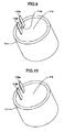
- Fig. 11 shows an exemplary configuration of a conventional ultrasonic sensor 10.
- the ultrasonic sensor 10 mainly includes a sensor case 11, a piezoelectric element 12 provided on a bottom part of the sensor case 11 and, using the bottom part of the sensor case 11 as a vibration plate, a terminal (conductive material) 13 in conductive connection with both electrodes situated on the upper and lower side of the piezoelectric element 12 while being connected to an external circuit of the sensor case 11, and a wire 14 connected to the terminal 13 and the piezoelectric element 12.
- the sensor case 11 has a configuration allowing a filling material 15 to be supplied therein for preventing liquid droplets from entering (See Japanese Laid-Open Patent Application Nos. 9-284896 , 11-266498 , 2000-32594 , and 2002-209294 ).
- a polarizing (poling) process process of applying a strong direct current electric field
- a polarizing (poling) process process of applying a strong direct current electric field
- the piezoelectric element in this example, a piezoelectric ceramic
- the piezoelectric ceramic attains a piezoelectric property.
- the poled piezoelectric ceramic has a characteristic of creating a voltage and causing polarization loss in a case where thermal change occurs in the poled piezoelectric ceramic (e.g., by application of heat).
- an embodiment of the present invention provides a method of manufacturing an ultrasonic sensor including a case, a piezoelectric element having first and second electrodes, and a conductive member having first and second conductive parts, the method including the steps of a) forming the conductive member by integrally forming the first and second conductive parts and a joining part that joins portions of the first and second conductive parts, b) mounting the piezoelectric element and the conductive member in the case so that the first conductive part is connected to the first electrode and the second conductive part is connected to the second electrode, and the joining part and the portions of the first and second conductive parts joined by the joining part are positioned outside of the case, c) supplying a filling material into the case, and d) removing the joining part after step c).
- the conductive member may be formed by using a cladding material.
- the step a) may include a step of punching out the conductive member from a planar conductive material.
- the method of manufacturing an ultrasonic sensor may further include a step of forming a notch part on each end of the joining part.
- Fig. 1 is a cross-sectional perspective view showing an ultrasonic sensor 100 according to an embodiment of the present invention.
- Fig. 2 is an exploded perspective view showing the ultrasonic sensor 100 according to an embodiment of the present invention.
- the ultrasonic sensor 100 which is manufactured by the manufacturing method according to an embodiment of the present invention includes, for example, an aluminum case (hereinafter referred to as "case") 111, a piezoelectric element 112, a conductive member 113 having first and second conductive parts 113a, 113b, a lead wire 114, acoustic material 118 (for example, see Fig. 8 ), filling material 119 (for example, see Fig. 8 ), and an epoxy adhesive agent (not shown).
- case aluminum case
- piezoelectric element 112 a conductive member 113 having first and second conductive parts 113a, 113b, a lead wire 114, acoustic material 118 (for example, see Fig. 8 ), filling material 119 (for example, see Fig. 8 ), and an epoxy adhesive agent (not shown).
- the case 111 is formed in a substantially cylindrical shape having an open top (open end) and a closed bottom (closed end). Because the piezoelectric element 112 generates ultrasonic waves by vibration, a material having good vibration characteristics is used in forming the case 111 (in this example, an aluminum material is used). As shown in Fig. 2 , a step part 111a is formed at an inner peripheral part of the case 111. The step part 111a serves to securely position the second conductive part 113b when mounting the conductive member 113 in the case 111.
- the piezoelectric element 112 converts between vibration (mechanical energy) and electrical energy in the ultrasonic sensor 100.
- the piezoelectric element 112 is formed of a crystal(s) of a ceramic material having a ferroelectric property.
- the piezoelectric element 112 is fabricated by performing a poling process on the ceramic crystal(s) by coating silver electrodes onto the upper and lower surfaces of the ceramic crystal(s) and applying high voltage to the ceramic crystal(s).
- the piezoelectric element 112 according to an embodiment of the present invention has an electrode 112a provided on its upper surface and another electrode 112b provided on its lower surface.
- the piezoelectric element 112 is installed in the case 111 in a manner facing the bottom surface of the case 111.
- the second electrode 112b provided on the lower surface of the piezoelectric element 112 becomes electrically connected to the case 111 when the piezoelectric element 112 is adhered to the bottom surface of the case 111. Furthermore, by welding one end of the second conductive part 113b to the case 111, connection between the other end of the second conductive part 113b and an external circuit can be realized.
- One end of the first conductive part 113a or one end of the lead wire 114 is connected to the first electrode 112a provided on the upper surface of the piezoelectric element 112 by directly soldering the one end of the first conductive part 113a or the lead wire 114 to the first electrode 112a provided on the upper surface of the piezoelectric element 112 or by using a conductive adhesive agent.
- the other end of the first conductive part 113a can be connected to an external circuit.
- the conductive member 113 is an input/output terminal of the ultrasonic sensor 100 for inputting signals to the ultrasonic sensor 100 and outputting signals from the ultrasonic sensor 100.
- the conductive member 113 is conductive with respect to the first and second electrodes 112a, 112b provided on the upper and lower surfaces of the piezoelectric element 112, to thereby realize connection with an external circuit.
- the conductive member 113 includes the first conductive part 113a and the second conductive part 113b. Although portions of the first conductive part 113a and the second conductive part 113b are joined by a joining part 113c (for example, see Fig. 1 ) at the time of forming the conductive member 113, the joining part 113c is separated from the first and second conductive parts 113a, 113b after completion of a supplying process (which includes a heating process) where the filling material 119 is supplied into the case 111.
- a supplying process which includes a heating process
- the piezoelectric element 112 and the conductive member 113 are mounted in the case 111 so that the first conductive part 113a is connected to the first electrode 112a and the second conductive part 113b is connected to the second electrode 112b, and the joining part 113c and the portions of the first and second conductive parts 113a, 113b joined by the joining part 113c are positioned outside of the case 111.
- the portion of the first and second conductive parts 113a, 113b are above the upper end of the case 111.
- the conductive member 113 is formed of a planar cladding material in which one side 115a is made of aluminum (aluminum side 115a) and the other side 115b is made of nickel (nickel side 115b).
- the overall configuration of the conductive member 113 is formed in an L-shape having a perpendicular part including a perpendicular plane and a bent part including a bent plane that is bent substantially 90 degrees with respect to the perpendicular part. That is, the bent plane is bent in such manner so as to fittingly engage the step part 111a of the case 111.
- the first conductive part 113a includes a perpendicular portion and a facing portion 116 which is formed by bending a part of the perpendicular portion in a manner facing the piezoelectric element 112.
- the second conductive part 113b includes a perpendicular portion and a bent portion.
- the bent portion of the second conductive part 113b includes a connecting part 117 for connecting to the case 111.
- the facing portion 116 of the first conductive part 113a is connected the electrode provided on the upper surface of the piezoelectric element 112 by attaching one end of the lead wire 114 to the facing portion 116 and the other end of the lead wire 114 to the electrode provided on the upper surface of the piezoelectric element 112. Thereby, the first conductive part 113a becomes electrically connected to the electrode 112a provided on the upper surface of the piezoelectric element 112.
- the connecting part 117 of the second conductive part 113b is connected to the case 111 by welding the connecting part 117 of the second conductive part 113b to the step part 111a of the case 111.
- the second conductive part 113b becomes electrically connected to the electrode 112b provided on the lower surface of the piezoelectric element 112. Accordingly, in view of good bonding characteristics with respect to aluminum (i.e. the case 111 formed of aluminum), the cladding material used in this embodiment of the present invention has one side formed of aluminum.
- the acoustic material 118 is formed of a resin material.
- the acoustic material 118 may be placed or laminated on the piezoelectric element 112. By placing the acoustic material 118 on the piezoelectric element 112, reverberation of the ultrasonic sensor 100 can be reduced and high sensitivity can be attained for the ultrasonic sensor 100.
- the filling material 119 is provided on top of the acoustic material 118.
- the filling material 119 is, for example, a thermosetting resin which is cured by applying heat thereto. Because such a heating process is performed on the filling material 119 when forming the filling material 119, the heat of the filling material 119 is also transmitted to the piezoelectric element 112. This may cause the above-described problem of polarization loss in the piezoelectric element 112.
- the case 111 is formed into a substantially cylindrical shape having a closed bottom (solid).
- the case 111 is formed by cutting aluminum material into such a shape-
- the step part 111a is formed inside the case 111.
- a poling process is performed on the piezoelectric element 112 by applying a silver electrode to both ends of the crystals of the ferroelectric material (in this embodiment, ceramic material) that form the piezoelectric element 112 and supplying high voltage to the piezoelectric element 112.
- the conductive member 113 includes: the first conductive part 113a; the second conductive part 113b; the joining part 113c for joining portions of the first and second conductive parts 113a, 113b; the facing part 116 for connecting to the electrode provided on the upper surface of the piezoelectric element 112; and the connecting part 117 for connecting to the step part 111a of the case 111.
- the first and second conductive parts 113a, 113b, the joining part 113c, the facing part 116, and the connecting part 117 are integrally formed into a united body by press-working the conductive member 113.
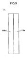
- the conductive member 113 including the first conductive part 113a, the second conductive part 113b, and the joining part 113c is formed by, for example, punching out the conductive member 113 from a planar conductive material by using a press (See Fig. 5 ).
- a press See Fig. 5
- a notch part 120 may be provided on each end of the joining part 113c so that the joining part 113c can be easily separated from the conductive member 113 after supplying the filling material 119 into the case 111.
- the connecting part 117 of the second conductive part 113b is bent to form the conductive member 113 into an L-shape.
- the connecting part 117 is bent in a manner so that the aluminum side 115a of the conductive member 113 is the side which connects to the case 111.
- the facing part 116 of the first conductive part 113a is bent in an opposite direction with respect to the connecting part 117 so that the facing part 116 faces the piezoelectric element 112.
- the facing part 116 is bent in a manner so that the plane of the facing part 116 facing the piezoelectric element 112 is the nickel side 115b of the conductive member 113.
- the conductive member 113 is inserted into the case 111. Then, the facing part 116 of the first conductive part 113a and one end of the lead wire 114 are soldered together. Then, the other end of the lead wire 114 and the electrode provided on the upper surface of the piezoelectric element 112 are soldered together.
- the welding method includes, for example, spot welding using a welding jig 112. Because the first conductive part 113a and the second conductive part 113b are joined together by the joining part 113c, there is no need to define the position of the first conductive part 113a when installing the conductive member 113 in the case 111.
- the connecting part 117 abuts the step part 111a of the case 111, the position of the first conductive part 113a and the position of the second conductive part 113b can be securely defined at the same time. Thereby, the conductive member 113 and the piezoelectric element 112 can be satisfactorily mounted in the case 111.
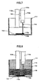
- Fig. 7 shows a step where the conductive member 113 and the piezoelectric element 112 are mounted in the case 111.
- Fig. 8 shows a step where the acoustic material 118 is provided in the case 111 subsequent to the step shown in Fig. 7 .
- the filling material 119 is supplied (inserted) into the case 111 as shown in Fig. 8 and 9 .
- the filling material 119 is supplied into the case 111
- portions of the first and second conductive parts 113a, 113b as well as the joining part 113c of the conductive member 113 are positioned outside of the case 111. This allows the joining part 113c to be cut off (removed) from the conductive member 113 after the process of supplying the filling material 119 into the case 111 is completed.
- the filling material 119 is cured, for example, by irradiating ultraviolet rays from the open end of the case 111.
- heat is also transmitted to the piezoelectric element 112, for example, from the heat of the filling material 119 or the heat generated by the heating process (curing process).
- the thermal change of the piezoelectric element 112 causes the piezoelectric element 112 to generate a voltage.
- the first and second conductive parts 113a and 113b which are connected to the piezoelectric element 112 are joined together by the joining part 113c, the first and second conductive parts 113a and 113b are electrically shorted.
- the joining part 113c is removed (cut off) from the conductive member 113 (see Figs. 8 and 10 ).
- polarization loss can easily be prevented by integrally forming the first and second conductive parts 113a, 113b together with the joining part 113c beforehand and removing the joining part 113c after supplying the filling material 119 into the case 111.
- the joining part 113c is to be removed after all of the other heating processes are completed, in order to prevent loss of polarization caused by thermal change of the piezoelectric element 112.
Landscapes
- Physics & Mathematics (AREA)
- General Physics & Mathematics (AREA)
- Engineering & Computer Science (AREA)
- Acoustics & Sound (AREA)
- Multimedia (AREA)
- Transducers For Ultrasonic Waves (AREA)
Applications Claiming Priority (1)
| Application Number | Priority Date | Filing Date | Title |
|---|---|---|---|
| JP2007155271A JP4900066B2 (ja) | 2007-06-12 | 2007-06-12 | 超音波センサの製造方法 |
Publications (2)
| Publication Number | Publication Date |
|---|---|
| EP2003430A2 true EP2003430A2 (de) | 2008-12-17 |
| EP2003430A3 EP2003430A3 (de) | 2010-08-04 |
Family
ID=39864716
Family Applications (1)
| Application Number | Title | Priority Date | Filing Date |
|---|---|---|---|
| EP20080251485 Withdrawn EP2003430A3 (de) | 2007-06-12 | 2008-04-22 | Verfahren zur Herstellung eines Ultraschallsensors |
Country Status (4)
| Country | Link |
|---|---|
| US (1) | US7587806B2 (de) |
| EP (1) | EP2003430A3 (de) |
| JP (1) | JP4900066B2 (de) |
| CN (1) | CN101325824A (de) |
Families Citing this family (14)
| Publication number | Priority date | Publication date | Assignee | Title |
|---|---|---|---|---|
| US7836769B2 (en) * | 2006-08-10 | 2010-11-23 | Akrion Systems Llc | Apparatus and method of measuring acoustical energy applied to a substrate |
| WO2008047743A1 (en) * | 2006-10-20 | 2008-04-24 | Murata Manufacturing Co., Ltd. | Ultrasonic sensor |
| CA3116787C (en) | 2010-06-16 | 2023-07-11 | Mueller International, Llc | Infrastructure monitoring devices, systems, and methods |
| US9772250B2 (en) | 2011-08-12 | 2017-09-26 | Mueller International, Llc | Leak detector and sensor |
| SG11201503041SA (en) | 2012-10-26 | 2015-05-28 | Mueller Int Llc | Detecting leaks in a fluid distribution system |
| US9528903B2 (en) | 2014-10-01 | 2016-12-27 | Mueller International, Llc | Piezoelectric vibration sensor for fluid leak detection |
| US10283857B2 (en) | 2016-02-12 | 2019-05-07 | Mueller International, Llc | Nozzle cap multi-band antenna assembly |
| US10305178B2 (en) | 2016-02-12 | 2019-05-28 | Mueller International, Llc | Nozzle cap multi-band antenna assembly |
| US10859462B2 (en) | 2018-09-04 | 2020-12-08 | Mueller International, Llc | Hydrant cap leak detector with oriented sensor |
| US11342656B2 (en) | 2018-12-28 | 2022-05-24 | Mueller International, Llc | Nozzle cap encapsulated antenna system |
| MY203968A (en) * | 2018-12-31 | 2024-07-26 | Sony Corp | Display device and speaker |
| US11473993B2 (en) | 2019-05-31 | 2022-10-18 | Mueller International, Llc | Hydrant nozzle cap |
| US11542690B2 (en) | 2020-05-14 | 2023-01-03 | Mueller International, Llc | Hydrant nozzle cap adapter |
| US12578245B2 (en) | 2022-10-28 | 2026-03-17 | Mueller International, Llc | Self-leveling sensor assembly |
Citations (4)
| Publication number | Priority date | Publication date | Assignee | Title |
|---|---|---|---|---|
| JPH09284896A (ja) | 1996-04-17 | 1997-10-31 | Murata Mfg Co Ltd | 超音波送受波器 |
| JPH11266498A (ja) | 1998-01-13 | 1999-09-28 | Murata Mfg Co Ltd | 超音波センサ、およびその製造方法 |
| JP2000032594A (ja) | 1998-04-24 | 2000-01-28 | Murata Mfg Co Ltd | 超音波送受波器 |
| JP2002209294A (ja) | 2001-01-10 | 2002-07-26 | Murata Mfg Co Ltd | 超音波センサ、これを備える電子機器および車両用バックソナー |
Family Cites Families (15)
| Publication number | Priority date | Publication date | Assignee | Title |
|---|---|---|---|---|
| JPS5790986A (en) * | 1980-11-26 | 1982-06-05 | Matsushita Electric Ind Co Ltd | Fabrication of piezo electric ceramic element |
| JPS61161446A (ja) * | 1985-01-10 | 1986-07-22 | Terumo Corp | 超音波探触子およびその製造方法 |
| JP3136628B2 (ja) * | 1991-03-22 | 2001-02-19 | 松下電器産業株式会社 | 圧電サウンダ |
| JPH0798589A (ja) * | 1993-09-28 | 1995-04-11 | Murata Mfg Co Ltd | 圧電ブザー |
| KR0165517B1 (ko) * | 1996-03-07 | 1999-05-01 | 김광호 | 진동 검출 센서 |
| DK172871B1 (da) * | 1997-08-22 | 1999-08-23 | Danfoss As | Ultralydstransducer |
| JPH11330578A (ja) * | 1998-05-20 | 1999-11-30 | Matsushita Electric Ind Co Ltd | 圧電素子並びにそれを用いた圧電振動子、発音体、圧電アクチュエータ、超音波探触子及び圧電トランス |
| JP3363834B2 (ja) * | 1999-06-07 | 2003-01-08 | 松下電器産業株式会社 | 多極コネクタおよび超音波探触子 |
| JP2001085259A (ja) * | 1999-09-09 | 2001-03-30 | Citizen Electronics Co Ltd | コイルとその製造方法 |
| JP2001128293A (ja) * | 1999-10-28 | 2001-05-11 | Murata Mfg Co Ltd | 圧電装置 |
| JP2002218578A (ja) * | 2001-01-22 | 2002-08-02 | Citizen Electronics Co Ltd | 多機能型発音体及びその製造方法 |
| JP4627400B2 (ja) * | 2002-08-29 | 2011-02-09 | 株式会社Neomaxマテリアル | アルミニウム/ニッケルクラッド材および電池用外部端子 |
| JP4048886B2 (ja) * | 2002-09-10 | 2008-02-20 | 株式会社村田製作所 | 超音波センサ |
| JP4230377B2 (ja) * | 2004-02-10 | 2009-02-25 | 株式会社Neomaxマテリアル | 端子用クラッド材およびその端子用クラッド材によって形成されたアルミニウム電線用端子 |
| JP4529889B2 (ja) * | 2005-02-10 | 2010-08-25 | セイコーエプソン株式会社 | 圧電振動体、圧電振動体の調整方法、圧電アクチュエータ、時計、電子機器 |
-
2007
- 2007-06-12 JP JP2007155271A patent/JP4900066B2/ja not_active Expired - Fee Related
-
2008
- 2008-03-26 CN CNA2008100878561A patent/CN101325824A/zh active Pending
- 2008-04-22 EP EP20080251485 patent/EP2003430A3/de not_active Withdrawn
- 2008-04-23 US US12/081,878 patent/US7587806B2/en not_active Expired - Fee Related
Patent Citations (4)
| Publication number | Priority date | Publication date | Assignee | Title |
|---|---|---|---|---|
| JPH09284896A (ja) | 1996-04-17 | 1997-10-31 | Murata Mfg Co Ltd | 超音波送受波器 |
| JPH11266498A (ja) | 1998-01-13 | 1999-09-28 | Murata Mfg Co Ltd | 超音波センサ、およびその製造方法 |
| JP2000032594A (ja) | 1998-04-24 | 2000-01-28 | Murata Mfg Co Ltd | 超音波送受波器 |
| JP2002209294A (ja) | 2001-01-10 | 2002-07-26 | Murata Mfg Co Ltd | 超音波センサ、これを備える電子機器および車両用バックソナー |
Also Published As
| Publication number | Publication date |
|---|---|
| EP2003430A3 (de) | 2010-08-04 |
| JP4900066B2 (ja) | 2012-03-21 |
| US7587806B2 (en) | 2009-09-15 |
| CN101325824A (zh) | 2008-12-17 |
| JP2008311735A (ja) | 2008-12-25 |
| US20080307623A1 (en) | 2008-12-18 |
Similar Documents
| Publication | Publication Date | Title |
|---|---|---|
| US7587806B2 (en) | Method of manufacturing an ultrasonic sensor | |
| US6445108B1 (en) | Piezoelectric acoustic component | |
| US20070105015A1 (en) | Battery and method of producing the same | |
| US7898151B2 (en) | Ultrasonic sensor having a piezoelectric element | |
| JP6891293B2 (ja) | 振動性ダイヤフラムに組み込まれた圧電セラミック変換素子を有する音響変換器 | |
| US20070228893A1 (en) | Piezoelectric Sounding Body | |
| CN100385999C (zh) | 表面安装电子元件封装 | |
| WO2007102460A1 (ja) | 超音波センサおよびその製造方法 | |
| KR100666976B1 (ko) | 초음파 탐촉자 및 그 제조 방법 | |
| JP3436205B2 (ja) | 圧電音響部品 | |
| JP4908411B2 (ja) | 圧力センサ及びその製造方法 | |
| JPH1032456A (ja) | 振動子 | |
| WO2006009220A1 (ja) | 超音波振動子 | |
| JP2001128293A (ja) | 圧電装置 | |
| JP3206915B2 (ja) | 超音波探触子 | |
| JP2000023296A (ja) | 超音波センサ | |
| JP3916013B2 (ja) | 超音波マイクロホンおよびその周波数調整方法 | |
| CN1913726B (zh) | 超声波装置及其组装方法 | |
| JP2010161528A (ja) | 圧電振動片、圧電振動片を用いた圧電振動子、および圧電振動片を用いた圧電デバイス | |
| JP3058517B2 (ja) | 高耐圧ハイドロフォン | |
| CN223642208U (zh) | 一种超声波换能器结构 | |
| JP3695098B2 (ja) | 圧力検出装置の製造方法 | |
| JP3189566B2 (ja) | ハンダ付状態の検査装置およびハンダ付状態の検査方法 | |
| KR20180123864A (ko) | 초음파 센서용 센서셀 | |
| JP2004228979A (ja) | 圧電振動子用パッケージおよび圧電振動子 |
Legal Events
| Date | Code | Title | Description |
|---|---|---|---|
| PUAI | Public reference made under article 153(3) epc to a published international application that has entered the european phase |
Free format text: ORIGINAL CODE: 0009012 |
|
| AK | Designated contracting states |
Kind code of ref document: A2 Designated state(s): AT BE BG CH CY CZ DE DK EE ES FI FR GB GR HR HU IE IS IT LI LT LU LV MC MT NL NO PL PT RO SE SI SK TR |
|
| AX | Request for extension of the european patent |
Extension state: AL BA MK RS |
|
| PUAL | Search report despatched |
Free format text: ORIGINAL CODE: 0009013 |
|
| AK | Designated contracting states |
Kind code of ref document: A3 Designated state(s): AT BE BG CH CY CZ DE DK EE ES FI FR GB GR HR HU IE IS IT LI LT LU LV MC MT NL NO PL PT RO SE SI SK TR |
|
| AX | Request for extension of the european patent |
Extension state: AL BA MK RS |
|
| 17P | Request for examination filed |
Effective date: 20100817 |
|
| AKX | Designation fees paid |
Designated state(s): DE |
|
| STAA | Information on the status of an ep patent application or granted ep patent |
Free format text: STATUS: THE APPLICATION IS DEEMED TO BE WITHDRAWN |
|
| 18D | Application deemed to be withdrawn |
Effective date: 20111102 |