EP2003548B1 - Ressourcenverwaltung in Mehrprozessorsystemen - Google Patents
Ressourcenverwaltung in Mehrprozessorsystemen Download PDFInfo
- Publication number
- EP2003548B1 EP2003548B1 EP08006412A EP08006412A EP2003548B1 EP 2003548 B1 EP2003548 B1 EP 2003548B1 EP 08006412 A EP08006412 A EP 08006412A EP 08006412 A EP08006412 A EP 08006412A EP 2003548 B1 EP2003548 B1 EP 2003548B1
- Authority
- EP
- European Patent Office
- Prior art keywords
- processor
- processor system
- primary
- primary processor
- status information
- Prior art date
- Legal status (The legal status is an assumption and is not a legal conclusion. Google has not performed a legal analysis and makes no representation as to the accuracy of the status listed.)
- Active
Links
Images

Classifications
-
- G—PHYSICS
- G06—COMPUTING OR CALCULATING; COUNTING
- G06F—ELECTRIC DIGITAL DATA PROCESSING
- G06F9/00—Arrangements for program control, e.g. control units
- G06F9/06—Arrangements for program control, e.g. control units using stored programs, i.e. using an internal store of processing equipment to receive or retain programs
- G06F9/30—Arrangements for executing machine instructions, e.g. instruction decode
- G06F9/38—Concurrent instruction execution, e.g. pipeline or look ahead
- G06F9/3877—Concurrent instruction execution, e.g. pipeline or look ahead using a secondary processor, e.g. coprocessor
-
- G—PHYSICS
- G06—COMPUTING OR CALCULATING; COUNTING
- G06F—ELECTRIC DIGITAL DATA PROCESSING
- G06F15/00—Digital computers in general; Data processing equipment in general
- G06F15/16—Combinations of two or more digital computers each having at least an arithmetic unit, a program unit and a register, e.g. for a simultaneous processing of several programs
- G06F15/163—Interprocessor communication
- G06F15/173—Interprocessor communication using an interconnection network, e.g. matrix, shuffle, pyramid, star, snowflake
- G06F15/17356—Indirect interconnection networks
- G06F15/17368—Indirect interconnection networks non hierarchical topologies
- G06F15/17375—One dimensional, e.g. linear array, ring
-
- G—PHYSICS
- G06—COMPUTING OR CALCULATING; COUNTING
- G06F—ELECTRIC DIGITAL DATA PROCESSING
- G06F9/00—Arrangements for program control, e.g. control units
- G06F9/06—Arrangements for program control, e.g. control units using stored programs, i.e. using an internal store of processing equipment to receive or retain programs
- G06F9/30—Arrangements for executing machine instructions, e.g. instruction decode
- G06F9/30094—Condition code generation, e.g. Carry, Zero flag
Definitions
- the present disclosure relates generally to the field of multi-processor systems and, more specifically, to techniques for resource management in multi-processor systems having a primary processor and pipelined secondary processors.
- a multi-processor system typically includes a primary processor administering a plurality of pipelined (i.e., connected in series) processors or co-processors, which are collectively referred to herein as secondary processors.
- the article "Multi-paradigm parallel programming" by Anthony Hey et al shown in Figure 2 such a linear chain.
- master-slave relationship may be formed between the primary processor and secondary processors.
- Such multi-processor systems may be used, for example, for processing of large amounts of video data or rendering graphics, among other computationally intensive applications.
- instructions and, occasionally, data blocks are forwarded by the primary or a respective intermediate secondary processor downstream to the adjacent secondary processor, and acknowledgements confirming completion of particular tasks (i.e., task status data) are communicated by the secondary processors upstream to the primary processor.
- the primary processor assigns new tasks to the secondary processors or re-allocates computational and memory resources in the system upon receipt of acknowledgements that the preceding tasks have been completed.
- At least one secondary processor is provided with a register containing status information for tasks executed by that secondary processor.
- the register is directly accessible by the primary processor via a dedicated data port of the secondary processor and a bus connecting the port to the primary processor.
- the register may be formed in a portion of a system memory that is directly accessible by the primary processor.
- the status information from intermediate secondary processors bypasses the upstream secondary processors and, as such, may be available to the primary processor in a real time.
- the disclosed techniques are used for managing computational and memory resources in multi-processor systems of wireless communication devices during execution of video applications, such as processing of video data or rendering graphics.
- FIG. 1 shows a block diagram of an exemplary multi-processor system.
- FIG. 2 shows a high-level block diagram of an exemplary pipelined processor of the system of FIG. 1 .
- FIG. 3 shows a flow diagram of a method for managing computational and memory resources in the system of FIG. 1 .
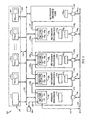
- FIG. 1 depicts a block diagram of an exemplary multi-processor system 100 in accordance with one embodiment of the present invention.
- the system 100 may be used for processing video data and/or rendering graphics, among other computationally intensive data processing applications.
- the system 100 is a portion of a graphics processing unit (GPU) of a wireless communication apparatus, such as a cellular phone, a video game console, a personal digital assistant (PDA), a laptop computer, an audio/video-enabled device (e.g., video-enabled MP3 player), and the like.
- GPU graphics processing unit
- PDA personal digital assistant
- MP3 player an audio/video-enabled device
- the GPU may be compliant, for example, with a document "OpenVG Specification, Version 1.0," July 28, 2005, which is publicly available. This document is a standard for 2D vector graphics suitable for handheld and mobile devices, such as cellular phones and other referred to above wireless communication apparatuses. Additionally, the GPU 402 may also be compliant with OpenGL2.0, OpenGL ES2.0, or D3D9.0 graphics standards.
- the system 100 illustratively includes a primary processor 110, a plurality of pipelined secondary processors 120 1 -120 K , a memory 130, an optional hardware graphics core 106, a memory bus 132, an acknowledgements bus 140, and system interfaces 102, 126 1 -126 K , and 107, where K is an integer and K ⁇ 2.
- the primary processor 110 and the secondary processors 120 1 -120 K are interconnected using the system interfaces 126 1 -126 K , and the secondary processor is connected to the hardware graphics core 106 using the system interface 107, respectively.
- at least one of the secondary processors 120 1 -120 K may be a portion of the hardware graphics core 106 or, alternatively, perform functions of the hardware graphics core 106.
- the primary processor 110, the pipelined secondary processors 120 1 -120 K , and hardware graphics core 106 may be formed on a single integrated circuit (IC). Such IC may be a portion of, for example, a system-on-chip (SoC) integrated circuit device of a wireless communication apparatus. Alternatively, the primary processor 110 and at least one of the secondary processors 120 1 -120 K or the hardware graphics core 106 or portions thereof may be formed on separate ICs.
- SoC system-on-chip
- each of the system interfaces 102, 126 1 -126 K , and 107 includes a command bus and, optionally, at least portions of data or address busses (not shown).
- the primary processor 110 and secondary processors 120 1 -120 K may also include sub-processors, internal memories, peripheral devices, support circuits, and the like elements, which are collectively referred to herein as modules 115 and 125 1 -125 K , respectively.
- the primary processor 110 comprises an input/output (I/O) module 118 including an input buffer (IB) 112 and an output buffer (OB) 114.
- each of the secondary processors 120 1 -120 K comprises a respective input/output (I/O) module 128 including an input buffer 122 and an output buffer 124.
- the I/O modules 118 and 128 1 -128 K facilitate communications within the system 100 or to/from the system 100.
- an input buffer 122 of a preceding (i.e., upstream) secondary processor 120 is connected to an output buffer 124 of the adjacent downstream secondary processor.
- an input buffer 122 2 of a secondary processor 120 2 is connected, via a system interface 126 2 , to an output buffer 124 1 of a secondary processor 120 1 .
- an output buffer 124 2 of the secondary processor 120 2 is connected, via a system interface 126 3 , to an input buffer 122 3 of a secondary processor 120 3 (not shown).
- the primary processor 110 may be connected to at least one of a remote processor, a network, or a user controls means, which are collectively shown as a means 104.
- the memory 130 generally includes a memory bank 111 of the primary processor 110, memory banks 121 1 -121 K of the respective the secondary processors 120 1 -120 K , and a memory bank 109 of the hardware graphics core 106.
- these memory banks together, form a shared memory block 134, which is accessible by the primary and secondary processors via a branch 131 (shown in phantom) of the memory bus 132.
- the input and output buffers 124 may contain additional references (pointers) to memory space jointly used by the respective secondary processors 120.
- the secondary processors 120 1 -120 K and the hardware graphics core 106 include respective status registers 142 1 -142 K+1 and data ports 144 1 -144 K+1 , and the primary processor 110 includes an input port 146.
- the status registers 142 1 -142 K+1 contain status information for tasks executed by the corresponding secondary processors 120 1 -120 K and the hardware graphics core 106.
- the hardware graphics core 106 may include the status registers 142 and the data ports 144.
- the data ports 144 1 -144 K+1 and the input port 146 are selectively coupled to the acknowledgements bus 140. Via the input port 144, the acknowledgements bus 140, and a respective data port 144, the primary processor 110 may directly access (i.e., read content of) the status registers 142.
- the acknowledgements bus 140 may be implemented as a direct input-output interface, for example, direct port or serial data input-output interface.
- the primary processor 110 may directly access the status registers 142 via a link 147 (shown in phantom) coupling the I/O module 118 to the acknowledgements bus 140.
- the status registers 142 may be accessed by remote processors (not shown), for example, processors monitoring performance of or debugging the system 100.
- the respective registers 142 may be formed (shown in phantom) in the memory banks 121 1 -121 K and 109.
- the registers 142 may be associated with the shared memory block 134.
- the memory bus 132 provides the primary processor 110 with a direct access to contents of at least the registers 142.
- FIG. 2 depicts a high-level block diagram of an exemplary pipelined secondary processor 120 of the system 100 of FIG. 1 in accordance with one embodiment of the present invention.
- the secondary processor 120 may be fabricated as a single IC, a portion thereof, or include several ICs.
- the secondary processor 120 may, for example, be a portion of a multi-processor GPU of a wireless communication apparatus, among other mobile or stationary video-enabled devices, as well as a portion of a networked server having architecture adapted for large-scale graphics processing.
- the secondary processor 120 includes a processing core 210, a program controller 220, a memory module 230, digital signal processing (DSP) circuits 240 comprising a plurality of arithmetic-logic units (ALUs) 242, the I/O module 128, the status register 142, and the data port 144.
- DSP digital signal processing
- the status register 142 may be a portion of the memory module 230.
- the memory module 230 includes a program memory 232, which contains one or more software modules that, in operation, define a content of the status register 142 and, via the data port 144, facilitate accessibility of the content by the primary processor 110 or other authorized user, as discussed above in reference to FIG. 1 .
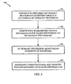
- FIG. 3 shows a flow diagram of a method 300 for managing computational and memory resources in the system 100 of FIG. 1 in accordance with one embodiment of the present invention.
- method steps of the method 300 are performed in the depicted order or at least two of these steps or portions thereof (e.g., steps 330 and 340) may be performed contemporaneously or in parallel.
- steps 330 and 340 may be performed contemporaneously or in parallel.
- the status registers 142 and data ports 144 are formed in the pipelined secondary processors 120 and the optional hardware graphics core 106 or the memory 130 of the multi-processor system 100, as discussed above in reference to FIG. 1 . Contents of the status registers 142 are directly accessible by the primary processor 110 of system 100.
- secondary processors 120 identify when particular tasks assigned or monitored by the primary processor 110 are completed. Upon completion of such a task, the corresponding status information is entered, in a predetermined data format, in the status register 142 of the respective secondary processor 120.
- the status information generally represents an acknowledgement, or confirmation, that the currently performed task is finished and, as such, the secondary processor and its computational and memory resources are available for the next task, as well as any resources of the primary processor that must be retained until completion of the task.
- such tasks may include repetitive cycles of processing graphics primitives, vertex buffer objects (VOBs), rendering video frames, and the like.
- the primary processor 110 selectively accesses the status registers 142 and, with a predetermined periodicity, acquires their contents.
- the status information from a pipelined secondary processor 120 bypasses upstream intermediate processors and becomes available to the primary processor 110 immediately upon completion of the respective task, i.e., in a real time.
- the status registers 142 formed in the memory banks 121 1 -121 K and 109 may directly be accessed by the primary processor 110 via the memory bus 130.
- the primary processor 110 analyzes the status information acquired from the status registers 142 and, in operation, manages computational and/or memory resources of the multi-processor system 100 based on that information.
- the primary processor 110 may allocate or re-allocate data between the respective memory blocks 111, 121 1 -121 K , and 109, selectively assign to or initiate new tasks in the respective secondary processors 120 or the hardware graphics core 106, and the like.
- the method 300 may be implemented in hardware, software, firmware, or any combination thereof in a form of a computer program product comprising one or more computer-executable instructions.
- the computer program product may be stored on or transmitted using a computer-readable medium, which includes computer storage medium and computer communication medium.
- the term "computer storage medium” refers herein to any medium adapted for storing the instructions that cause the computer to execute the method.
- the computer storage medium may comprise solid-sate memory devices, including electronic memory devices (e.g., RAM, ROM, EEPROM, and the like), optical memory devices (e.g., compact discs (CD), digital versatile discs (DVD), and the like), or magnetic memory devices (e.g., hard drives, flash drives, tape drives, and the like), or other memory devices adapted to store the computer program product, or a combination of such memory devices.
- the term "computer communication medium” refers herein to any physical interface adapted to transmit the computer program product from one place to another using for example, a modulated carrier wave, an optical signal, a DC or AC current, and the like means.
- the computer communication medium may comprise twisted wire pairs, printed or flat cables, coaxial cables, fiber-optic cables, digital subscriber lines (DSL), or other wired, wireless, or optical serial or parallel interfaces, or a combination thereof.
- aspects of the present invention are illustratively described within the context of the processors of a multi-processor graphics pipeline. It will be appreciated by those skilled in the art that the invention may also be utilized within the context of other multi-processor systems having pipelined processors/co-processors, which are administered by one or more supervisory processor. Management of computational or memory resources in such systems using the techniques discussed above in reference to FIGS. 1-3 has been contemplated and is within the scope of the present invention.
- the invention may be used in cellular phones, video game consoles, PDAs, laptop computers, MP3 players and other graphics-enabled mobile or stationary devices having multi-processor architectures.
Landscapes
- Engineering & Computer Science (AREA)
- Theoretical Computer Science (AREA)
- Software Systems (AREA)
- Physics & Mathematics (AREA)
- General Engineering & Computer Science (AREA)
- General Physics & Mathematics (AREA)
- Computer Hardware Design (AREA)
- Mathematical Physics (AREA)
- Image Processing (AREA)
- Image Generation (AREA)
- Multi Processors (AREA)
- Hardware Redundancy (AREA)
Claims (16)
- Ein Multiprozessorsystem (100) aufweisend einen Primärprozessor (110), eine Vielzahl von in Pipeline angeordneten Sekundärprozessoren (120), Systemschnittstellen (126), die den Primärprozessor (110) und die Vielzahl von Sekundärprozessoren (120) in Serie verbinden um Aufgaben weiterzuleiten, zugewiesen von dem Primärprozessor (110) an einen Sekundärprozessor von dem Primärprozessor abwärts an den Sekundärprozessor (120),
dadurch gekennzeichnet, dass
das Multiprozessorsystem (100) weiter Mittel aufweist, das direkt zugreifbar für den Primärprozessor (110) ist, jedes Mittel beinhaltet Statusinformationen für Aufgaben, die von einem jeweiligen Sekundärprozessor ausgeführt werden, und einen Bus (132, 140), der den Primärprozessor (110) mit direktem Zugang zu den Statusinformationen in dem Mittel versorgt und Aufwärts-Sekundärprozessoren (120) umgeht, somit wird dem Primärprozessor ermöglicht direkt die Statusinformationen von dem Mittel zu beschaffen um rechnerische und/oder Speicher-Ressourcen zu verwalten, basierend auf den Statusinformationen. - Das Multiprozessorsystem (100) nach Anspruch 1, wobei das Mittel ein Register (142) ist.
- Das Multiprozessorsystem (100) nach Anspruch 2, wobei der zumindest eine Sekundärprozessor (120) einen Port (146) aufweist um auf das Register (142) zuzugreifen.
- Das Multiprozessorsystem (100) nach Anspruch 3, wobei der Bus (140) an den Port (146) gekoppelt ist und zugreifbar für den Primärprozessor (110) ist.
- Das Multiprozessorsystem (100) nach Anspruch 4, wobei der Primärprozessor (110) an den Bus (140) gekoppelt ist.
- Das Multiprozessorsystem (100) nach Anspruch 4, wobei der Bus (140) an zumindest einen entfernten Prozessor gekoppelt ist.
- Das Multiprozessorsystem (100) nach Anspruch 2, wobei das Register (142) ein Teil von einem Speichermodul (230) von dem zumindest einen Sekundärprozessor (120) ist.
- Das Multiprozessorsystem (100) nach Anspruch 2, wobei das Register (142) ein Teil von einem Speicher von dem Multiprozessorsystem (100) ist.
- Das Multiprozessorsystem (100) nach Anspruch 1, wobei der zumindest einen Sekundärprozessor (120) ein Teil von einem Graphikhardwarekern von dem Multiprozessorsystem ist.
- Das Multiprozessorsystem (100) nach Anspruch 1, wobei das Multiprozessorsystem (100) ein Teil von einem System-auf-Chip (SoC) integrierten Schaltungsgeräts ist.
- Das Multiprozessorsystem (100) nach Anspruch 1, wobei das Multiprozessorsystem (100) ein Teil von einer drahtlosen Kommunikationsvorrichtung ist, ausgewählt von der Gruppe bestehend aus einem Mobiltelefon, einer Videospielkonsole, eines Persönlichen Digitalen Assistenten (PDA), eines Laptop Computers, und eines Audio/Video-Ermöglichten Gerätes, oder ein Teil von einem stationären Video-Ermöglichten Gerätes, oder ein Teil von einem Server.
- Das Multiprozessorsystem (100) nach einem der Ansprüche 1 bis 9 und 11, wobei das Multiprozessorsystem (100) ein Teil von einem integrierten Schaltkreis ist.
- Ein Verfahren zum Verwalten von rechnerischen und/oder Speicher-Ressourcen in einem Multiprozessorsystem (100) umfassend einen Primärprozessor (110) und eine Vielzahl von in Pipeline angeordneten Sekundärprozessoren (120), wobei Systemschnittstellen (126) den Primärprozessor (110) und die Vielzahl von Sekundärprozessoren (120) in Serie verbinden um Aufgaben weiterzuleiten, zugewiesen von dem Primärprozessor (110) an einen Sekundärprozessor von dem Primärprozessor abwärts an den Sekundärprozessor (120), und wobei das Multiprozessorsystem (100) Mittel umfasst, das Statusinformationen beinhaltet für Aufgaben, die von einem jeweiligen Sekundärprozessor (120) ausgeführt werden, aufweisend:Benutzen eines Bus (132, 140) um den Primärprozessor (110) mit direktem Zugang zu den Statusinformationen in dem Mittel zu versorgen und Aufwärts-Sekundärprozessoren (120) zu umgehen; undVerwalten, mittels des Primärprozessors, von rechnerischen und/oder Speicher-Ressourcen von dem Multiprozessorsystem (100), basierend auf den Statusinformationen.
- Das Verfahren nach Anspruch 13, wobei das Mittel ein Register (142) ist.
- Das Verfahren nach Anspruch 14, wobei das Register (142) zumindest in einigen von den Sekundärprozessoren (120) oder Speichern (230) davon oder in einem Speicher von dem Multiprozessorsystem (100) ist.
- Ein Computerprogrammprodukt umfassend ein computerlesbares Medium, welches Instruktionen hat ein Verfahren nach einem der Ansprüche 13 bis 15 auszuführen.
Applications Claiming Priority (1)
| Application Number | Priority Date | Filing Date | Title |
|---|---|---|---|
| US11/763,377 US7669036B2 (en) | 2007-06-14 | 2007-06-14 | Direct path monitoring by primary processor to each status register in pipeline chained secondary processors for task allocation via downstream communication |
Publications (2)
| Publication Number | Publication Date |
|---|---|
| EP2003548A1 EP2003548A1 (de) | 2008-12-17 |
| EP2003548B1 true EP2003548B1 (de) | 2011-03-23 |
Family
ID=39512786
Family Applications (1)
| Application Number | Title | Priority Date | Filing Date |
|---|---|---|---|
| EP08006412A Active EP2003548B1 (de) | 2007-06-14 | 2008-03-31 | Ressourcenverwaltung in Mehrprozessorsystemen |
Country Status (6)
| Country | Link |
|---|---|
| US (1) | US7669036B2 (de) |
| EP (1) | EP2003548B1 (de) |
| AT (1) | ATE503222T1 (de) |
| DE (1) | DE602008005671D1 (de) |
| TW (1) | TW200907699A (de) |
| WO (1) | WO2008154552A1 (de) |
Cited By (2)
| Publication number | Priority date | Publication date | Assignee | Title |
|---|---|---|---|---|
| US20120185623A1 (en) * | 2011-01-14 | 2012-07-19 | Skyworks Solutions, Inc. | Apparatus and methods for serial interfaces |
| US10437774B2 (en) | 2017-01-26 | 2019-10-08 | Skyworks Solutions, Inc. | Low noise serial interfaces with gated clock |
Families Citing this family (29)
| Publication number | Priority date | Publication date | Assignee | Title |
|---|---|---|---|---|
| US7962553B2 (en) * | 2006-07-31 | 2011-06-14 | Hewlett-Packard Development Company, L.P. | Method and system for distribution of maintenance tasks in a multiprocessor computer system |
| US8359365B2 (en) | 2008-02-11 | 2013-01-22 | Nuix Pty Ltd | Systems and methods for load-balancing by secondary processors in parallel document indexing |
| US9785700B2 (en) * | 2008-02-11 | 2017-10-10 | Nuix Pty Ltd | Systems and methods for load-balancing by secondary processors in parallelized indexing |
| US9928260B2 (en) | 2008-02-11 | 2018-03-27 | Nuix Pty Ltd | Systems and methods for scalable delocalized information governance |
| US9621366B2 (en) * | 2008-12-18 | 2017-04-11 | Telefonaktiebolaget Lm Ericsson (Publ) | Network node and method for controlling resources in a communication network |
| KR101640848B1 (ko) * | 2009-12-28 | 2016-07-29 | 삼성전자주식회사 | 멀티코어 시스템 상에서 단위 작업을 할당하는 방법 및 그 장치 |
| TW201243714A (en) * | 2011-04-22 | 2012-11-01 | Feature Integration Technology Inc | A method and a system for dispatching the execution sequence of the processes in a multiprocessor system |
| CN103810139B (zh) * | 2014-01-24 | 2017-04-26 | 浙江众合科技股份有限公司 | 一种多处理器的数据交换方法和装置 |
| US9665372B2 (en) | 2014-05-12 | 2017-05-30 | International Business Machines Corporation | Parallel slice processor with dynamic instruction stream mapping |
| US9672043B2 (en) | 2014-05-12 | 2017-06-06 | International Business Machines Corporation | Processing of multiple instruction streams in a parallel slice processor |
| US10826930B2 (en) | 2014-07-22 | 2020-11-03 | Nuix Pty Ltd | Systems and methods for parallelized custom data-processing and search |
| US9760375B2 (en) | 2014-09-09 | 2017-09-12 | International Business Machines Corporation | Register files for storing data operated on by instructions of multiple widths |
| US9720696B2 (en) | 2014-09-30 | 2017-08-01 | International Business Machines Corporation | Independent mapping of threads |
| US9977678B2 (en) | 2015-01-12 | 2018-05-22 | International Business Machines Corporation | Reconfigurable parallel execution and load-store slice processor |
| US10133576B2 (en) | 2015-01-13 | 2018-11-20 | International Business Machines Corporation | Parallel slice processor having a recirculating load-store queue for fast deallocation of issue queue entries |
| US10133581B2 (en) | 2015-01-13 | 2018-11-20 | International Business Machines Corporation | Linkable issue queue parallel execution slice for a processor |
| US10175885B2 (en) * | 2015-01-19 | 2019-01-08 | Toshiba Memory Corporation | Memory device managing data in accordance with command and non-transitory computer readable recording medium |
| US11200249B2 (en) | 2015-04-16 | 2021-12-14 | Nuix Limited | Systems and methods for data indexing with user-side scripting |
| US9983875B2 (en) | 2016-03-04 | 2018-05-29 | International Business Machines Corporation | Operation of a multi-slice processor preventing early dependent instruction wakeup |
| US10037211B2 (en) | 2016-03-22 | 2018-07-31 | International Business Machines Corporation | Operation of a multi-slice processor with an expanded merge fetching queue |
| US10346174B2 (en) | 2016-03-24 | 2019-07-09 | International Business Machines Corporation | Operation of a multi-slice processor with dynamic canceling of partial loads |
| US10761854B2 (en) | 2016-04-19 | 2020-09-01 | International Business Machines Corporation | Preventing hazard flushes in an instruction sequencing unit of a multi-slice processor |
| US10037229B2 (en) | 2016-05-11 | 2018-07-31 | International Business Machines Corporation | Operation of a multi-slice processor implementing a load/store unit maintaining rejected instructions |
| US9934033B2 (en) | 2016-06-13 | 2018-04-03 | International Business Machines Corporation | Operation of a multi-slice processor implementing simultaneous two-target loads and stores |
| US10042647B2 (en) | 2016-06-27 | 2018-08-07 | International Business Machines Corporation | Managing a divided load reorder queue |
| US10318419B2 (en) | 2016-08-08 | 2019-06-11 | International Business Machines Corporation | Flush avoidance in a load store unit |
| US10944814B1 (en) * | 2017-12-04 | 2021-03-09 | Amazon Technologies, Inc. | Independent resource scheduling for distributed data processing programs |
| US10963385B2 (en) * | 2019-01-18 | 2021-03-30 | Silicon Motion Technology (Hong Kong) Limited | Method and apparatus for performing pipeline-based accessing management in a storage server with aid of caching metadata with cache module which is hardware pipeline module during processing object write command |
| US11232049B2 (en) | 2019-12-13 | 2022-01-25 | Micron Technology, Inc. | Memory module with computation capability |
Family Cites Families (9)
| Publication number | Priority date | Publication date | Assignee | Title |
|---|---|---|---|---|
| US3868805A (en) * | 1971-04-26 | 1975-03-04 | Usm Corp | Double glazing unit |
| GB9019025D0 (en) * | 1990-08-31 | 1990-10-17 | Ncr Co | Work station having multiprocessing capability |
| US6341324B1 (en) | 1995-10-06 | 2002-01-22 | Lsi Logic Corporation | Exception processing in superscalar microprocessor |
| US6392654B1 (en) * | 1998-09-01 | 2002-05-21 | Ati Technologies | Method and apparatus for processing data with improved concurrency |
| US6829697B1 (en) * | 2000-09-06 | 2004-12-07 | International Business Machines Corporation | Multiple logical interfaces to a shared coprocessor resource |
| US6865631B2 (en) * | 2000-12-14 | 2005-03-08 | International Business Machines Corporation | Reduction of interrupts in remote procedure calls |
| US7073048B2 (en) | 2002-02-04 | 2006-07-04 | Silicon Lease, L.L.C. | Cascaded microcomputer array and method |
| US6963613B2 (en) * | 2002-04-01 | 2005-11-08 | Broadcom Corporation | Method of communicating between modules in a decoding system |
| US7827386B2 (en) * | 2003-06-30 | 2010-11-02 | Intel Corporation | Controlling memory access devices in a data driven architecture mesh array |
-
2007
- 2007-06-14 US US11/763,377 patent/US7669036B2/en active Active
-
2008
- 2008-03-31 AT AT08006412T patent/ATE503222T1/de not_active IP Right Cessation
- 2008-03-31 EP EP08006412A patent/EP2003548B1/de active Active
- 2008-03-31 DE DE602008005671T patent/DE602008005671D1/de active Active
- 2008-06-10 WO PCT/US2008/066453 patent/WO2008154552A1/en not_active Ceased
- 2008-06-13 TW TW097122254A patent/TW200907699A/zh unknown
Cited By (7)
| Publication number | Priority date | Publication date | Assignee | Title |
|---|---|---|---|---|
| US20120185623A1 (en) * | 2011-01-14 | 2012-07-19 | Skyworks Solutions, Inc. | Apparatus and methods for serial interfaces |
| US9189430B2 (en) * | 2011-01-14 | 2015-11-17 | Skyworks Solutions, Inc. | Apparatus and methods for serial interfaces |
| US9606947B2 (en) | 2011-01-14 | 2017-03-28 | Skyworks Solutions, Inc. | Apparatus and methods for serial interfaces |
| US10402356B2 (en) | 2011-01-14 | 2019-09-03 | Skyworks Solutions, Inc. | Apparatus and methods for serial interfaces |
| US10437774B2 (en) | 2017-01-26 | 2019-10-08 | Skyworks Solutions, Inc. | Low noise serial interfaces with gated clock |
| US10963418B2 (en) | 2017-01-26 | 2021-03-30 | Skyworks Solutions, Inc. | Low noise serial interfaces with gated clock |
| US11314685B2 (en) | 2017-01-26 | 2022-04-26 | Skyworks Solutions, Inc. | Low noise serial interfaces with gated clock |
Also Published As
| Publication number | Publication date |
|---|---|
| US7669036B2 (en) | 2010-02-23 |
| ATE503222T1 (de) | 2011-04-15 |
| DE602008005671D1 (de) | 2011-05-05 |
| EP2003548A1 (de) | 2008-12-17 |
| US20080313380A1 (en) | 2008-12-18 |
| WO2008154552A1 (en) | 2008-12-18 |
| TW200907699A (en) | 2009-02-16 |
Similar Documents
| Publication | Publication Date | Title |
|---|---|---|
| EP2003548B1 (de) | Ressourcenverwaltung in Mehrprozessorsystemen | |
| CN107704922B (zh) | 人工神经网络处理装置 | |
| AU2003287320B2 (en) | Pipeline accelerator and related system and method | |
| CN100562892C (zh) | 图像处理引擎及包含图像处理引擎的图像处理系统 | |
| US20190026158A1 (en) | Virtual vector processing | |
| AU765469B2 (en) | Shared memory type vector processing system and control method thereof | |
| US10700968B2 (en) | Optimized function assignment in a multi-core processor | |
| US20070174509A1 (en) | System for asynchronous dma command completion notification | |
| CN104126179B (zh) | 用于多核处理器中的核心间通信的方法和装置 | |
| US20040015970A1 (en) | Method and system for data flow control of execution nodes of an adaptive computing engine (ACE) | |
| US20180107484A1 (en) | Implementing conflict-free instructions for concurrent operation on a processor | |
| CN103777923A (zh) | Dma向量缓冲区 | |
| US20180109452A1 (en) | Latency guaranteed network on chip | |
| CN107729267B (zh) | 资源的分散分配以及用于支持由多个引擎执行指令序列的互连结构 | |
| CN106095604A (zh) | 一种多核处理器的核间通信方法及装置 | |
| CN115129480A (zh) | 标量处理单元的访问控制方法及标量处理单元 | |
| US8902915B2 (en) | Dataport and methods thereof | |
| CN111324439A (zh) | 用于向量单元的密码引擎和调度方法 | |
| US9703614B2 (en) | Managing a free list of resources to decrease control complexity and reduce power consumption | |
| CN111258769B (zh) | 数据传输装置和方法 | |
| US20130080746A1 (en) | Providing A Dedicated Communication Path Separate From A Second Path To Enable Communication Between Complaint Sequencers Of A Processor Using An Assertion Signal | |
| CN111240745A (zh) | 交叉执行的增强型标量向量双管线架构 | |
| US12399849B2 (en) | Data processing methods, apparatuses, electronic devices and computer-readable storage media | |
| CN105683914A (zh) | 改进图形处理单元上的链式任务的性能的方法和装置 | |
| Lim et al. | Shared Memory Model over a Switchless PCIe NTB Interconnect Network. |
Legal Events
| Date | Code | Title | Description |
|---|---|---|---|
| PUAI | Public reference made under article 153(3) epc to a published international application that has entered the european phase |
Free format text: ORIGINAL CODE: 0009012 |
|
| AK | Designated contracting states |
Kind code of ref document: A1 Designated state(s): AT BE BG CH CY CZ DE DK EE ES FI FR GB GR HR HU IE IS IT LI LT LU LV MC MT NL NO PL PT RO SE SI SK TR |
|
| AX | Request for extension of the european patent |
Extension state: AL BA MK RS |
|
| 17P | Request for examination filed |
Effective date: 20090604 |
|
| 17Q | First examination report despatched |
Effective date: 20090710 |
|
| AKX | Designation fees paid |
Designated state(s): AT BE BG CH CY CZ DE DK EE ES FI FR GB GR HR HU IE IS IT LI LT LU LV MC MT NL NO PL PT RO SE SI SK TR |
|
| GRAP | Despatch of communication of intention to grant a patent |
Free format text: ORIGINAL CODE: EPIDOSNIGR1 |
|
| GRAS | Grant fee paid |
Free format text: ORIGINAL CODE: EPIDOSNIGR3 |
|
| GRAA | (expected) grant |
Free format text: ORIGINAL CODE: 0009210 |
|
| AK | Designated contracting states |
Kind code of ref document: B1 Designated state(s): AT BE BG CH CY CZ DE DK EE ES FI FR GB GR HR HU IE IS IT LI LT LU LV MC MT NL NO PL PT RO SE SI SK TR |
|
| REG | Reference to a national code |
Ref country code: GB Ref legal event code: FG4D |
|
| REG | Reference to a national code |
Ref country code: CH Ref legal event code: EP |
|
| REG | Reference to a national code |
Ref country code: IE Ref legal event code: FG4D |
|
| REF | Corresponds to: |
Ref document number: 602008005671 Country of ref document: DE Date of ref document: 20110505 Kind code of ref document: P |
|
| REG | Reference to a national code |
Ref country code: DE Ref legal event code: R096 Ref document number: 602008005671 Country of ref document: DE Effective date: 20110505 |
|
| REG | Reference to a national code |
Ref country code: NL Ref legal event code: VDEP Effective date: 20110323 |
|
| PG25 | Lapsed in a contracting state [announced via postgrant information from national office to epo] |
Ref country code: GR Free format text: LAPSE BECAUSE OF FAILURE TO SUBMIT A TRANSLATION OF THE DESCRIPTION OR TO PAY THE FEE WITHIN THE PRESCRIBED TIME-LIMIT Effective date: 20110624 Ref country code: LV Free format text: LAPSE BECAUSE OF FAILURE TO SUBMIT A TRANSLATION OF THE DESCRIPTION OR TO PAY THE FEE WITHIN THE PRESCRIBED TIME-LIMIT Effective date: 20110323 Ref country code: HR Free format text: LAPSE BECAUSE OF FAILURE TO SUBMIT A TRANSLATION OF THE DESCRIPTION OR TO PAY THE FEE WITHIN THE PRESCRIBED TIME-LIMIT Effective date: 20110323 Ref country code: LT Free format text: LAPSE BECAUSE OF FAILURE TO SUBMIT A TRANSLATION OF THE DESCRIPTION OR TO PAY THE FEE WITHIN THE PRESCRIBED TIME-LIMIT Effective date: 20110323 Ref country code: SE Free format text: LAPSE BECAUSE OF FAILURE TO SUBMIT A TRANSLATION OF THE DESCRIPTION OR TO PAY THE FEE WITHIN THE PRESCRIBED TIME-LIMIT Effective date: 20110323 |
|
| LTIE | Lt: invalidation of european patent or patent extension |
Effective date: 20110323 |
|
| PG25 | Lapsed in a contracting state [announced via postgrant information from national office to epo] |
Ref country code: BG Free format text: LAPSE BECAUSE OF FAILURE TO SUBMIT A TRANSLATION OF THE DESCRIPTION OR TO PAY THE FEE WITHIN THE PRESCRIBED TIME-LIMIT Effective date: 20110623 Ref country code: AT Free format text: LAPSE BECAUSE OF FAILURE TO SUBMIT A TRANSLATION OF THE DESCRIPTION OR TO PAY THE FEE WITHIN THE PRESCRIBED TIME-LIMIT Effective date: 20110323 Ref country code: CY Free format text: LAPSE BECAUSE OF FAILURE TO SUBMIT A TRANSLATION OF THE DESCRIPTION OR TO PAY THE FEE WITHIN THE PRESCRIBED TIME-LIMIT Effective date: 20110323 Ref country code: NO Free format text: LAPSE BECAUSE OF FAILURE TO SUBMIT A TRANSLATION OF THE DESCRIPTION OR TO PAY THE FEE WITHIN THE PRESCRIBED TIME-LIMIT Effective date: 20110623 Ref country code: SI Free format text: LAPSE BECAUSE OF FAILURE TO SUBMIT A TRANSLATION OF THE DESCRIPTION OR TO PAY THE FEE WITHIN THE PRESCRIBED TIME-LIMIT Effective date: 20110323 |
|
| PG25 | Lapsed in a contracting state [announced via postgrant information from national office to epo] |
Ref country code: BE Free format text: LAPSE BECAUSE OF FAILURE TO SUBMIT A TRANSLATION OF THE DESCRIPTION OR TO PAY THE FEE WITHIN THE PRESCRIBED TIME-LIMIT Effective date: 20110323 |
|
| PG25 | Lapsed in a contracting state [announced via postgrant information from national office to epo] |
Ref country code: MC Free format text: LAPSE BECAUSE OF NON-PAYMENT OF DUE FEES Effective date: 20110331 Ref country code: PT Free format text: LAPSE BECAUSE OF FAILURE TO SUBMIT A TRANSLATION OF THE DESCRIPTION OR TO PAY THE FEE WITHIN THE PRESCRIBED TIME-LIMIT Effective date: 20110725 Ref country code: EE Free format text: LAPSE BECAUSE OF FAILURE TO SUBMIT A TRANSLATION OF THE DESCRIPTION OR TO PAY THE FEE WITHIN THE PRESCRIBED TIME-LIMIT Effective date: 20110323 |
|
| REG | Reference to a national code |
Ref country code: HU Ref legal event code: AG4A Ref document number: E011474 Country of ref document: HU |
|
| PG25 | Lapsed in a contracting state [announced via postgrant information from national office to epo] |
Ref country code: ES Free format text: LAPSE BECAUSE OF FAILURE TO SUBMIT A TRANSLATION OF THE DESCRIPTION OR TO PAY THE FEE WITHIN THE PRESCRIBED TIME-LIMIT Effective date: 20110704 Ref country code: IS Free format text: LAPSE BECAUSE OF FAILURE TO SUBMIT A TRANSLATION OF THE DESCRIPTION OR TO PAY THE FEE WITHIN THE PRESCRIBED TIME-LIMIT Effective date: 20110723 Ref country code: SK Free format text: LAPSE BECAUSE OF FAILURE TO SUBMIT A TRANSLATION OF THE DESCRIPTION OR TO PAY THE FEE WITHIN THE PRESCRIBED TIME-LIMIT Effective date: 20110323 Ref country code: CZ Free format text: LAPSE BECAUSE OF FAILURE TO SUBMIT A TRANSLATION OF THE DESCRIPTION OR TO PAY THE FEE WITHIN THE PRESCRIBED TIME-LIMIT Effective date: 20110323 Ref country code: RO Free format text: LAPSE BECAUSE OF FAILURE TO SUBMIT A TRANSLATION OF THE DESCRIPTION OR TO PAY THE FEE WITHIN THE PRESCRIBED TIME-LIMIT Effective date: 20110323 |
|
| PG25 | Lapsed in a contracting state [announced via postgrant information from national office to epo] |
Ref country code: MT Free format text: LAPSE BECAUSE OF FAILURE TO SUBMIT A TRANSLATION OF THE DESCRIPTION OR TO PAY THE FEE WITHIN THE PRESCRIBED TIME-LIMIT Effective date: 20110323 Ref country code: NL Free format text: LAPSE BECAUSE OF FAILURE TO SUBMIT A TRANSLATION OF THE DESCRIPTION OR TO PAY THE FEE WITHIN THE PRESCRIBED TIME-LIMIT Effective date: 20110323 |
|
| REG | Reference to a national code |
Ref country code: IE Ref legal event code: MM4A |
|
| PLBE | No opposition filed within time limit |
Free format text: ORIGINAL CODE: 0009261 |
|
| STAA | Information on the status of an ep patent application or granted ep patent |
Free format text: STATUS: NO OPPOSITION FILED WITHIN TIME LIMIT |
|
| PG25 | Lapsed in a contracting state [announced via postgrant information from national office to epo] |
Ref country code: IE Free format text: LAPSE BECAUSE OF NON-PAYMENT OF DUE FEES Effective date: 20110331 |
|
| 26N | No opposition filed |
Effective date: 20111227 |
|
| PG25 | Lapsed in a contracting state [announced via postgrant information from national office to epo] |
Ref country code: DK Free format text: LAPSE BECAUSE OF FAILURE TO SUBMIT A TRANSLATION OF THE DESCRIPTION OR TO PAY THE FEE WITHIN THE PRESCRIBED TIME-LIMIT Effective date: 20110323 Ref country code: PL Free format text: LAPSE BECAUSE OF FAILURE TO SUBMIT A TRANSLATION OF THE DESCRIPTION OR TO PAY THE FEE WITHIN THE PRESCRIBED TIME-LIMIT Effective date: 20110323 |
|
| REG | Reference to a national code |
Ref country code: DE Ref legal event code: R097 Ref document number: 602008005671 Country of ref document: DE Effective date: 20111227 |
|
| PG25 | Lapsed in a contracting state [announced via postgrant information from national office to epo] |
Ref country code: IT Free format text: LAPSE BECAUSE OF FAILURE TO SUBMIT A TRANSLATION OF THE DESCRIPTION OR TO PAY THE FEE WITHIN THE PRESCRIBED TIME-LIMIT Effective date: 20110323 |
|
| REG | Reference to a national code |
Ref country code: CH Ref legal event code: PL |
|
| PG25 | Lapsed in a contracting state [announced via postgrant information from national office to epo] |
Ref country code: CH Free format text: LAPSE BECAUSE OF NON-PAYMENT OF DUE FEES Effective date: 20120331 Ref country code: LI Free format text: LAPSE BECAUSE OF NON-PAYMENT OF DUE FEES Effective date: 20120331 |
|
| PG25 | Lapsed in a contracting state [announced via postgrant information from national office to epo] |
Ref country code: LU Free format text: LAPSE BECAUSE OF NON-PAYMENT OF DUE FEES Effective date: 20110331 |
|
| PG25 | Lapsed in a contracting state [announced via postgrant information from national office to epo] |
Ref country code: TR Free format text: LAPSE BECAUSE OF FAILURE TO SUBMIT A TRANSLATION OF THE DESCRIPTION OR TO PAY THE FEE WITHIN THE PRESCRIBED TIME-LIMIT Effective date: 20110323 |
|
| REG | Reference to a national code |
Ref country code: FR Ref legal event code: PLFP Year of fee payment: 9 |
|
| REG | Reference to a national code |
Ref country code: FR Ref legal event code: PLFP Year of fee payment: 10 |
|
| REG | Reference to a national code |
Ref country code: FR Ref legal event code: PLFP Year of fee payment: 11 |
|
| PGFP | Annual fee paid to national office [announced via postgrant information from national office to epo] |
Ref country code: FI Payment date: 20180223 Year of fee payment: 11 Ref country code: GB Payment date: 20180223 Year of fee payment: 11 |
|
| PGFP | Annual fee paid to national office [announced via postgrant information from national office to epo] |
Ref country code: FR Payment date: 20180223 Year of fee payment: 11 Ref country code: HU Payment date: 20180223 Year of fee payment: 11 |
|
| PG25 | Lapsed in a contracting state [announced via postgrant information from national office to epo] |
Ref country code: FI Free format text: LAPSE BECAUSE OF NON-PAYMENT OF DUE FEES Effective date: 20190331 |
|
| GBPC | Gb: european patent ceased through non-payment of renewal fee |
Effective date: 20190331 |
|
| REG | Reference to a national code |
Ref country code: DE Ref legal event code: R082 Ref document number: 602008005671 Country of ref document: DE Representative=s name: BARDEHLE PAGENBERG PARTNERSCHAFT MBB PATENTANW, DE Ref country code: DE Ref legal event code: R081 Ref document number: 602008005671 Country of ref document: DE Owner name: QUALCOMM INCORPORATED, SAN DIEGO, US Free format text: FORMER OWNER: QUALCOMM INC., SAN DIEGO, CALIF., US |
|
| PG25 | Lapsed in a contracting state [announced via postgrant information from national office to epo] |
Ref country code: GB Free format text: LAPSE BECAUSE OF NON-PAYMENT OF DUE FEES Effective date: 20190331 Ref country code: HU Free format text: LAPSE BECAUSE OF NON-PAYMENT OF DUE FEES Effective date: 20190401 |
|
| PG25 | Lapsed in a contracting state [announced via postgrant information from national office to epo] |
Ref country code: FR Free format text: LAPSE BECAUSE OF NON-PAYMENT OF DUE FEES Effective date: 20190331 |
|
| PGFP | Annual fee paid to national office [announced via postgrant information from national office to epo] |
Ref country code: DE Payment date: 20250210 Year of fee payment: 18 |