EP2003603A2 - Transpondeur et procédé destiné au fonctionnement d'un transpondeur - Google Patents
Transpondeur et procédé destiné au fonctionnement d'un transpondeur Download PDFInfo
- Publication number
- EP2003603A2 EP2003603A2 EP08010591A EP08010591A EP2003603A2 EP 2003603 A2 EP2003603 A2 EP 2003603A2 EP 08010591 A EP08010591 A EP 08010591A EP 08010591 A EP08010591 A EP 08010591A EP 2003603 A2 EP2003603 A2 EP 2003603A2
- Authority
- EP
- European Patent Office
- Prior art keywords
- threshold
- capacitor
- transponder
- arithmetic unit
- routines
- Prior art date
- Legal status (The legal status is an assumption and is not a legal conclusion. Google has not performed a legal analysis and makes no representation as to the accuracy of the status listed.)
- Withdrawn
Links
Images
Classifications
-
- G—PHYSICS
- G06—COMPUTING OR CALCULATING; COUNTING
- G06K—GRAPHICAL DATA READING; PRESENTATION OF DATA; RECORD CARRIERS; HANDLING RECORD CARRIERS
- G06K19/00—Record carriers for use with machines and with at least a part designed to carry digital markings
- G06K19/06—Record carriers for use with machines and with at least a part designed to carry digital markings characterised by the kind of the digital marking, e.g. shape, nature, code
- G06K19/067—Record carriers with conductive marks, printed circuits or semiconductor circuit elements, e.g. credit or identity cards also with resonating or responding marks without active components
- G06K19/07—Record carriers with conductive marks, printed circuits or semiconductor circuit elements, e.g. credit or identity cards also with resonating or responding marks without active components with integrated circuit chips
- G06K19/0723—Record carriers with conductive marks, printed circuits or semiconductor circuit elements, e.g. credit or identity cards also with resonating or responding marks without active components with integrated circuit chips the record carrier comprising an arrangement for non-contact communication, e.g. wireless communication circuits on transponder cards, non-contact smart cards or RFIDs
-
- G—PHYSICS
- G06—COMPUTING OR CALCULATING; COUNTING
- G06K—GRAPHICAL DATA READING; PRESENTATION OF DATA; RECORD CARRIERS; HANDLING RECORD CARRIERS
- G06K19/00—Record carriers for use with machines and with at least a part designed to carry digital markings
- G06K19/06—Record carriers for use with machines and with at least a part designed to carry digital markings characterised by the kind of the digital marking, e.g. shape, nature, code
- G06K19/067—Record carriers with conductive marks, printed circuits or semiconductor circuit elements, e.g. credit or identity cards also with resonating or responding marks without active components
- G06K19/07—Record carriers with conductive marks, printed circuits or semiconductor circuit elements, e.g. credit or identity cards also with resonating or responding marks without active components with integrated circuit chips
- G06K19/0701—Record carriers with conductive marks, printed circuits or semiconductor circuit elements, e.g. credit or identity cards also with resonating or responding marks without active components with integrated circuit chips at least one of the integrated circuit chips comprising an arrangement for power management
- G06K19/0707—Record carriers with conductive marks, printed circuits or semiconductor circuit elements, e.g. credit or identity cards also with resonating or responding marks without active components with integrated circuit chips at least one of the integrated circuit chips comprising an arrangement for power management the arrangement being capable of collecting energy from external energy sources, e.g. thermocouples, vibration, electromagnetic radiation
-
- G—PHYSICS
- G06—COMPUTING OR CALCULATING; COUNTING
- G06K—GRAPHICAL DATA READING; PRESENTATION OF DATA; RECORD CARRIERS; HANDLING RECORD CARRIERS
- G06K19/00—Record carriers for use with machines and with at least a part designed to carry digital markings
- G06K19/06—Record carriers for use with machines and with at least a part designed to carry digital markings characterised by the kind of the digital marking, e.g. shape, nature, code
- G06K19/067—Record carriers with conductive marks, printed circuits or semiconductor circuit elements, e.g. credit or identity cards also with resonating or responding marks without active components
- G06K19/07—Record carriers with conductive marks, printed circuits or semiconductor circuit elements, e.g. credit or identity cards also with resonating or responding marks without active components with integrated circuit chips
- G06K19/0701—Record carriers with conductive marks, printed circuits or semiconductor circuit elements, e.g. credit or identity cards also with resonating or responding marks without active components with integrated circuit chips at least one of the integrated circuit chips comprising an arrangement for power management
- G06K19/0712—Record carriers with conductive marks, printed circuits or semiconductor circuit elements, e.g. credit or identity cards also with resonating or responding marks without active components with integrated circuit chips at least one of the integrated circuit chips comprising an arrangement for power management the arrangement being capable of triggering distinct operating modes or functions dependent on the strength of an energy or interrogation field in the proximity of the record carrier
Definitions
- the present invention relates to a transponder and a method for operating a transponder and a use for a transponder.
- the DE 698 31 711 T2 shows a transponder communication device, which is designed for contactless communication with a present in a receiving area of the transponder communication device transponder. Furthermore, the shows DE 698 31 711 T2 a transponder configured for contactless communication with at least one transponder communication device and activated in an active state for communicating with a transponder communication device.
- the US 5,339,073 discloses an access control system including an interrogation unit that issues an interrogation signal and a plurality of transponders, each transponder having a stored identity code that is different from that of the other transponders.
- This identity code contains a plurality of fields, each of which holds a selected info message bit.
- the interrogation signal is controlled in such a way that at the same time the fields of all transponders located in the area are queried serially. Any one of the transponders having a bit match in the polled field requested by the polling signal will sent back to the interrogation unit a group response signal.
- the interrogation unit is designed to determine the identity of each valid transponder in the range from the series of received response signals.
- a system and method is known in which energy is saved in the operation of a transponder.
- the transponder is activated or woken up in a plurality of stages.
- a threshold detector measures the energy level of the received RF energy. When the RF energy exceeds a predetermined threshold, the transponder uses the modulation detector to check whether it has been awakened by a valid signal or by a random sudden change in amplitude (burst). When a predetermined modulation has been detected, the transponder is fully activated to its normal operating condition.
- a method for transmitting data between a base station and a passive transponder is disclosed in the document EP 473 569 B1 known.
- digital data is exchanged between a base station and a passive transponder by means of an amplitude-modulated carrier wave.
- the invention is based on the object to provide a method that improves the power supply of a transponder as possible.
- the transponder has a capacitor for storing energy transmitted via an air interface and a computer unit that can be supplied with the stored energy. If the transponder is supplied with energy transmitted via an air interface, such a transponder is also referred to as a passive transponder. In addition, the transponder can have its own power supply - such as a rechargeable or non-rechargeable battery.
- a capacitor voltage of the capacitor is compared to a first threshold.
- a comparator can be used.
- the voltage of the capacitor is sampled and converted analog-digital.
- an analog comparator can be used, which allows a continuous comparison.
- the capacitor voltage is compared with a second threshold, wherein the first threshold and the second threshold differ.
- a comparator can be used for comparison of the capacitor voltage with the second threshold. The comparison with the first threshold and with the second threshold may be disjoint in time, but preferably at the same time.
- the arithmetic unit preferably executes a number of routines with different prioritization.
- the first operating mode is defined when the capacitor voltage is above the first threshold.
- the capacitor voltage is meant the amount, so that it is irrelevant whether the capacitor voltage is considered positive or negative voltage.
- the operating mode is preferably determined by the arithmetic unit, for example by setting certain values or parameters.
- the operating mode is preferably dependent on the capacitor voltage advantageously detected by a comparator.
- a signal associated with the detection or coded is transmitted to the arithmetic unit.
- the signal is, for example, a detection status flag or interrupt signal (IRQ).
- IRQ detection status flag or interrupt signal
- a status register programmed within the arithmetic unit is updated according to the detection within a software program.
- routines - such as interrupt routines (IRQ) - associated with the second threshold have a higher priority than routines associated with the first threshold.
- Routines of higher prioritization can for example pre-allocate interruptions of the program sequence which are otherwise assigned to routines of lower prioritization.
- a suspension of the routines of the arithmetic unit takes place.
- the exposure occurs under the condition that the capacitor voltage is below the second threshold.
- register values of the routines are stored, for example, in a non-volatile memory (EEPROM, FRAM, etc.) and the values can be reloaded into registers after exposure.
- the previously exposed routines are continued when the capacitor voltage is again above the first threshold or already above the second threshold. If the arithmetic unit is reset, an initialization is started first and then the routines are processed from the beginning.
- the suspended routines can be continued anywhere within their course. Preferably, at least one of the suspended routines will continue at the location within its course to which it has previously been suspended. Alternatively, returns within the course of the respective routine are also possible. Therefore, to continue the routine, it will not be restarted or initialized.
- first interrupt signal (English interrupt request) for interrupting the program sequence in the computing unit.
- the interrupt signal arrives at an interruptible input of the arithmetic unit.
- the interrupt signal is generated, for example, as a rising edge of a digital signal.
- falling below and / or exceeding the second threshold by the capacitor voltage triggers a second interrupt signal for interrupting the program sequence in the computing unit.
- the invention is further based on the object to provide a use for a transponder whose power supply is improved as possible.
- a use of a first threshold and a second threshold different from the first threshold for monitoring a capacitor voltage of a capacitor of a transponder is provided.
- the transponder has, in addition to the capacitor, a computing unit which can be supplied with energy stored in the capacitor.
- the arithmetic unit is designed to reduce the current consumption when the capacitor voltage is between the first threshold and the second threshold.
- the computing unit preferably operates in a first operating mode when the capacitor voltage is above the first threshold.
- the first operating mode can also be referred to as normal mode.
- the functionality of the arithmetic unit and / or the transponder is not limited.
- the computing unit preferably operates in a second operating mode when the capacitor voltage is below the first threshold and above a second threshold.
- the second operating mode can also be referred to as a warning mode (warning level).
- at least one limitation of a current drain from the capacitor is activated.
- at least one functionality of the transponder is deactivated in order to reduce the current drain from the capacitor.
- firmware periodically reads a status register programmed within the arithmetic unit that contains the operating mode.
- peripheral circuits of the transponder are activated or deactivated or a clock frequency of the arithmetic unit is changed.
- the arithmetic unit operates in a third mode of operation when the capacitor voltage is below the second threshold.
- the third operating mode may also be referred to as an emergency operating mode (switch-off level).
- the majority of the functionality of the transponder is deactivated in the third operating mode. Only a small charge has remained in the capacitor.
- the arithmetic unit advantageously changes to a sleep state.
- the routines of the arithmetic unit are suspended. The suspended routines may be continued at any point within their course - for example, at the exposed point or elsewhere by return - when the capacitor voltage is at least above the second threshold.
- a third threshold is additionally provided below the second threshold.
- the arithmetic unit is reset when the capacitor voltage falls below the third threshold (reset level). For example, the capacitor voltage in the third operating mode, despite the deactivation of the majority of the functionality of the transponder by a very low current drain from the capacitor continue to fall and fall below the third threshold.
- a reset of the arithmetic unit to avoid undefined states. If the capacitor voltage rises again after the reset, the arithmetic unit is first initialized and then all routines are restarted.
- the invention is further based on the object to provide a transponder whose power supply is improved as possible.
- a transponder is provided with a transmit-receive circuit, with a capacitor, with a computing unit and with a comparison circuit.
- the capacitor is connected to the transceiver circuit for charging.
- the arithmetic unit is connected to the power supply to the capacitor.
- the arithmetic unit is directly or indirectly connected to the transceiver circuit for transmitting data.
- the comparison circuit is connected to the capacitor. Furthermore, the arithmetic unit is connected to the comparison circuit.
- the comparison circuit is arranged to compare a capacitor voltage of the capacitor with a first threshold and with a second threshold different from the first threshold. Preferably, the capacitor voltage can be applied as an input to an input of the comparison circuit.
- the first threshold and / or the second threshold have a hysteresis.
- the comparison circuit for the first threshold preferably has a first window comparator or Schmitt trigger and / or a second window comparator or Schmitt trigger for the second threshold.
- the hysteresis has a voltage window with respect to the capacitor voltage, in which the operating mode is not changed. If, for example, the lower threshold hysteresis level is reached for the first threshold, the arithmetic unit changes, for example, from the first operating mode to the second operating mode. If, for example, the capacitor voltage then rises slightly, with the upper hysteresis level of the first threshold not yet exceeded, then the arithmetic unit remains in the second operating mode.
- the arithmetic unit is preferably set up to execute a number of routines with different prioritization within their program sequence.
- the arithmetic unit is set up in response to an output signal of the comparison circuit to stop a number of low priority routines and to continue a number of high priority routines.
- the computer unit is set up in dependence on the output signal of the comparison circuit to disconnect peripheral circuits from the power supply from the capacitor or to reduce the frequency of the clock signal of the arithmetic unit.
- the transponder additionally has a battery and a switch.
- the switch is connected to the battery and to the capacitor for switching the power supply between the battery and the capacitor.
- the battery is rechargeable, for example.
- the arithmetic unit is arranged to control the switching of the power supply in response to an output signal of the comparison circuit.
- a further subcircuit of the transponder may be provided to control the switching.
- the first threshold and / or the second threshold of the comparison circuit are adjustable.
- the setting can be effected by a signal via the transmit-receive circuit or by a control of the arithmetic unit.
- the setting of the first and / or second threshold dynamically, for example, depending on the boundary condition of the transponder.
- a self-learning setting for example by means of evaluation by the arithmetic unit is possible.
- the arithmetic unit for setting the first threshold and / or the second threshold is formed and connected to a control input of the comparison circuit.
- the comparison circuit has a multiplexer.
- a first input of the multiplexer is connected to the capacitor and a second input of the multiplexer is connected to a battery, in particular for measuring the battery voltage.
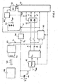
- Fig. 1 a simplified schematic representation of a transponder is shown.
- a base station 100 which is connectable to the transponder via an air interface.
- the base station 100 transmits an alternating magnetic field 120, which can be received by the transceiver circuit 20 with a transponder coil L t .
- the received energy of the alternating magnetic field 120 is converted into a charging current I C , which charges a capacitor C buf .
- the capacitor C buf is discharged by the discharge current I D.
- the magnetic alternating field 120 also serves for bidirectional data transmission between the transponder and the base station 100.
- the discharge current I D is used to supply a computing unit 10 and further subcircuit 12, 20, 30, 31, 40, 41, 50 with electrical energy.
- a connected to the capacitor C buf voltage regulator 30 is provided which provides a supply voltage Vdd at its output.
- the voltage regulator 30 is connected via a switch 31 to the supply voltage connection of the arithmetic unit 10.
- the arithmetic unit 10 is, for example, a computational core of a microcontroller.
- the capacitor C buf is charged so that the capacitor voltage V C increases. If, on the other hand, the discharge current I D exceeds the charging current I C , the capacitor C buf is discharged so that the capacitor voltage V c drops. The capacitor voltage V c thus depends on the difference between charging current I C and discharge current I D. If the capacitor voltage V C is too low, the arithmetic unit 10 can no longer reliably execute the program routines of a program sequence. The error rate increases with decreasing capacitor voltage V C and can abort the program flow and the Reset the arithmetic unit 10 lead. Unregistered register values of the arithmetic unit 10 are lost during the reset.
- the transponder has a comparison circuit 40.
- the comparison circuit 40 has, for example, a number of comparators.
- An input voltage V in of the comparison circuit 40 is compared by the comparison circuit with a first threshold and a second threshold.
- the first threshold and the second threshold are different.
- the first threshold and the second threshold are in the embodiment of Fig. 1 adjustable.
- the first threshold and the second threshold are each set in a voltage range of the capacitor voltage V C in which the arithmetic unit 10 is still working reliably.
- the first threshold and / or the second threshold hysteresis in order to avoid constantly changing states in case of a fluctuation of the capacitor voltage V C in the region of the respective threshold.
- the operating modes allow the surprising effect that the current drain during operation of the transponder can be optimized as a passive transponder by selectively activating or deactivating specific functionalities of the transponder during operation. The activation or deactivation is dependent on the capacitor voltage V C of the capacitor C buf .
- One or more operating modes for reduced current drain for passive transponder applications serve as early indicators and warnings for the software running in the computing unit 10 of a dangerously low supply voltage Vdd before the capacitor voltage V c drops below a reset threshold. When resetting, all values currently determined in the arithmetic unit 10 go lost.
- a reset of the arithmetic unit 10 is undesirable because the reset forces the arithmetic unit 10 to restart initialization routines and return to the initial state. This in turn requires the base station 100 to again send an initialization signal to the transponder to begin data transmission from the beginning.
- the comparison circuit 40 is connected via a switchable inverter 12 to inputs of the arithmetic unit 10, which allow an interruption of the program flow in the arithmetic unit 10.
- the first threshold is the output signal A and the second threshold associated with the output signal B.
- the switchable inverter 12 the output signal A can be inverted or not inverted in response to the control signal D.
- the output signal B can be inverted or not inverted in response to the control signal D.
- the switched output signals A 'and B' are applied to the inputs of the arithmetic unit 10.
- Fig. 1 are the connections between the comparison circuit 40 and the.
- Arithmetic unit 10 executed in triplicate, so that three input signals V in three channels can be monitored simultaneously with the same or different first and second thresholds.
- comparison circuit 40 is connected to at least one output of the arithmetic unit 10.
- the comparison circuit 40 is formed with adjustable thresholds, so that at least one threshold is adjustable by the arithmetic unit 10 and in particular changeable during operation of the transponder.
- the comparison circuit 40 may further comprise a multiplexer 41 to switch a plurality of voltages to be monitored to the input V in .
- a multiplexer 41 to switch a plurality of voltages to be monitored to the input V in .
- Fig. 1 is an entrance of the Multiplexer 41 with the capacitor C buf and another input connected to a battery 21, so that the battery voltage V bat can be monitored.
- a number of further inputs of the multiplexer 41 may be provided. For example, a voltage proportional to the amplitude of the alternating magnetic field can be monitored (in FIG Fig. 1 not shown).
- the battery 21 to charge the battery 21 to the capacitor C buf connectable. The connection is advantageously carried out as a function of the current operating mode. For example, the battery 21 is charged only when the capacitor voltage V C is above the first threshold, since then a sufficient energy transfer from the base station 100 is ensured to the transponder.
- the switch 31 of the embodiment of Fig. 1 is connected to the battery 21 and the voltage regulator 30 and allows switching between a power supply from the capacitor C buf and the charging current I C and a power supply from the battery V bat .
- the switch 31 is formed for example by two alternately switchable field effect transistors.
- a control circuit 50 is provided, whose output is connected to the switch 31 and to read the switching state to the arithmetic unit 10. Furthermore, inputs of the control circuit 50 are connected to the arithmetic unit 10 and / or the output of the comparison circuit 40.
- control circuit 50 Another input of the control circuit 50 is connected to the transmission-reception circuit 20. This allows the switch-on circuit 20 to switch 31 when the transmission is active and the received energy is sufficient for the program flow in the arithmetic unit 10.
- the connection of the control circuit 50 to the arithmetic unit 10 allows the software of the arithmetic unit 10 to directly control the switch 31 when the mode of operation is identified.
- control circuit 50 is connected to the comparison circuit 40 such that by means of a signal of the comparison circuit 40 is switched directly between the capacitor voltage V C and battery voltage V bat . This function is only activated if the battery voltage V bat is available.
- a reset logic 60 is connected via an OR gate 61 to a reset input RST of the arithmetic unit 10. If the voltage supply Vdd of the arithmetic unit 10 is too low, so that undefined states can arise, the arithmetic unit 10 is reset by the reset logic 60 applying a reset signal to the reset input RST of the arithmetic unit 10 via the OR gate 61. Thereafter, the arithmetic unit 10 is reinitialized and all routines are restarted. Likewise the data transmission with the base station 100 must be started from the beginning.
- the OR gate 61 is connected to the control circuit 50, so that by an input signal to the control circuit 50 by the arithmetic unit 10 itself and / or by the comparison circuit 40 and / or by the transmit-receive circuit 20, a reset of the arithmetic unit 10 initiated could be.
- the invention is not limited to the illustrated embodiment of the transponder in Fig. 1 limited.
- the invention includes a variety of different modifications.
- the battery 21, the voltage regulator 30, the switch 31, the control circuit 50, the inverter 12, the OR gate 61, the reset logic 60 and / or the multiplexer 41 may be omitted.
- Fig. 1 Fixed, non-adjustable thresholds can be used.
- transponder circuit according to Fig. 1 can be used particularly advantageously for a motor vehicle key, wherein transmission conditions for the alternating magnetic field 120 varies greatly with time.
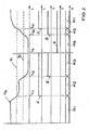
- Fig. 2 is a diagram with a functionality of a voltage monitoring for a transponder by the mapping of multiple waveforms shown schematically.
- the quantities V in , A ', B' and D refer to the corresponding quantities in Fig. 1 , Alternatively, however, another than the one in Fig. 1 shown.
- Transponder circuit with an in Fig. 2 shown functionality can be used.
- the upper part of the diagram shows the variation of the input voltage V in to be compared with respect to a first threshold V 1 and a second threshold V 2 .
- the time is plotted with respect to all signals.
- the arithmetic unit 10 processes a number of routines in the program sequence in the associated first operating mode M1, the routines having a different prioritization.
- the signal A changes to a second operating mode M2.
- the second operating mode M2 may also be referred to as a low power mode. In this second mode of operation M2, a number of low priority routines are stopped and a number of high priority routines are continued. Therefore, at least one routine of low prioritization is stopped and at least one routine of high prioritization is continued.
- Routines of high prioritization are, for example, routines whose register values must be saved. These register values are needed to read the stored register values back into register after a voltage dip - if the capacitor voltage V ln is again sufficient to continue the routines - and to continue the program sequence. This causes the surprising effect that a communication does not have to be completely carried out again after a connection abort, but a continuation of the communication is enabled according to the state before the connection abort.
- low priority routines are stopped. This causes the surprising effect that the period in which reliable execution of the program routines of the program sequence is possible is extended. This is achieved by the capacitor voltage V C, even without a charging current I C , ie slower without magnetic alternating field. The error rate is reduced.
- the current drain from the capacitor C buf can surprisingly be significantly reduced by the computing unit 10. This lengthens the time between the two times t 11 and t 12 and thus the length of the operating mode M2.
- the arithmetic unit 10 changes to a third operating mode M3.
- This third mode of operation M3 may also be referred to as a sleep mode.
- the input voltage V in can decrease to such an extent that no further operation in the arithmetic unit 10 can take place, or it can occur in the arithmetic unit 10 undefined states arise. In this case, a reset can be carried out so that all register values in the arithmetic unit 10 are deleted.
- the switchable inverter 12 is switched at the time t 3 with the signal D, so that the signal A 'is now inverted to the signal A and so that the signal B' is now inverted to the signal B.
- Falling edges of the signals A and B could also be used to interrupt the program sequence in the arithmetic unit 10.
- the input voltage V in rises again above the first threshold V 1 .
- the arithmetic unit 10 can subsequently start all the high and low priority routines again in the operating mode M1.
- the signal D is again set to a low value in the first operating mode M1 (not shown).
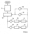
- Fig. 3 shows a simplified schematic flowchart of a program flow in the computing unit 10 with monitoring of the capacitor voltage V C.
- the capacitor C buf is loaded in the program part 71 and the data input at the transponder is checked.
- the arithmetic unit 10 is reset and an initialization routine is started.
- routine part 72 all higher and lower priority routines are started in a first mode of operation. Falling below a first threshold, a first interrupt signal 73 is generated and the program flow is interrupted. The fixed or dynamic address of the interrupt routine is loaded. Subsequently, the program flow is continued in a second operating mode in the program part 71.
- a second interrupt signal 74 is generated and the fixed or dynamic address of the interrupt routine is loaded.
- the arithmetic unit 10 in a third operating mode - a sleep mode - offset. In the third mode of operation, after execution of the last instructions, all routines may be suspended to continue with restored power.
- the program flow returns to the program portion 72, with the execution of the higher priority routines and the low priority routines back.
- the invention is not based on the embodiment of a process sequence Fig. 3 limited. In this way, it is easy for the person skilled in the art to derive other program flows which nevertheless have the monitoring function of the two thresholds for the three operating modes.
- the four interrupt signals may also be dynamically assigned four different and variable thresholds depending on the address within the program flow. It is also possible to provide further thresholds beyond the two thresholds in order, for example, to control the current drain by the arithmetic unit in several increments.
Landscapes
- Engineering & Computer Science (AREA)
- Computer Hardware Design (AREA)
- Microelectronics & Electronic Packaging (AREA)
- Physics & Mathematics (AREA)
- General Physics & Mathematics (AREA)
- Theoretical Computer Science (AREA)
- Electromagnetism (AREA)
- Computer Networks & Wireless Communication (AREA)
- Near-Field Transmission Systems (AREA)
Applications Claiming Priority (1)
| Application Number | Priority Date | Filing Date | Title |
|---|---|---|---|
| DE102007027610A DE102007027610A1 (de) | 2007-06-12 | 2007-06-12 | Transponder, Verfahren zum Betrieb eines Transponders |
Publications (2)
| Publication Number | Publication Date |
|---|---|
| EP2003603A2 true EP2003603A2 (fr) | 2008-12-17 |
| EP2003603A3 EP2003603A3 (fr) | 2010-01-13 |
Family
ID=39926981
Family Applications (1)
| Application Number | Title | Priority Date | Filing Date |
|---|---|---|---|
| EP08010591A Withdrawn EP2003603A3 (fr) | 2007-06-12 | 2008-06-11 | Transpondeur et procédé destiné au fonctionnement d'un transpondeur |
Country Status (4)
| Country | Link |
|---|---|
| US (1) | US8718545B2 (fr) |
| EP (1) | EP2003603A3 (fr) |
| JP (1) | JP2008312210A (fr) |
| DE (1) | DE102007027610A1 (fr) |
Cited By (1)
| Publication number | Priority date | Publication date | Assignee | Title |
|---|---|---|---|---|
| WO2019074690A1 (fr) * | 2017-10-10 | 2019-04-18 | Tyco Fire & Security Gmbh | Systèmes et procédés d'exploitation d'étiquettes |
Families Citing this family (14)
| Publication number | Priority date | Publication date | Assignee | Title |
|---|---|---|---|---|
| US20090237219A1 (en) * | 2008-03-21 | 2009-09-24 | Berlin Bradley M | Security apparatus, system and method of using same |
| US8630584B2 (en) * | 2008-11-26 | 2014-01-14 | Nationz Technologies Inc. | RF SIM card, card reader, and communication method |
| DE102009013962A1 (de) | 2009-03-20 | 2010-10-14 | Texas Instruments Deutschland Gmbh | Leistungspegelindikator |
| ATE537514T1 (de) | 2009-04-07 | 2011-12-15 | Nxp Bv | Rfid-vorrichtung, die in einem ersten und einem zweiten betriebsstatus bedienbar ist |
| DE102009021329B4 (de) * | 2009-05-14 | 2018-02-01 | Texas Instruments Deutschland Gmbh | Halbduplex-RFID-Transponder und Verfahren zum Betreiben eines Halbduplex-RFID-Transponders |
| KR101813011B1 (ko) | 2011-05-27 | 2017-12-28 | 삼성전자주식회사 | 무선 전력 및 데이터 전송 시스템 |
| JP5787830B2 (ja) * | 2012-06-01 | 2015-09-30 | 株式会社東芝 | 受電装置および送受電システム |
| US9128690B2 (en) * | 2012-09-24 | 2015-09-08 | Texas Instruments Incorporated | Bus pin reduction and power management |
| TWI468704B (zh) * | 2012-11-19 | 2015-01-11 | Ind Tech Res Inst | 中介層的測試方法 |
| WO2017205176A1 (fr) | 2016-05-23 | 2017-11-30 | X-Card Holdings, Llc | Carte électronique à interfaces multiples |
| US11551537B2 (en) | 2019-04-11 | 2023-01-10 | Nexite Ltd. | Wireless dual-mode identification tag |
| CN115001539A (zh) | 2019-04-11 | 2022-09-02 | 奈克赛特公司 | 配置为利用采集的能量进行传输供能的无线装置 |
| EP4275160B1 (fr) | 2021-01-11 | 2025-05-07 | Nexite Ltd. | Opérations sans contact et automatiques d'un magasin de vente au détail |
| EP4449301A1 (fr) | 2021-12-13 | 2024-10-23 | Nexite Ltd. | Systèmes, procédés et dispositifs pour le fonctionnement sans contact et automatique de magasins de vente au détail |
Citations (4)
| Publication number | Priority date | Publication date | Assignee | Title |
|---|---|---|---|---|
| US5339073A (en) | 1987-03-31 | 1994-08-16 | Identec Limited | Access control equipment and method for using the same |
| US5345231A (en) | 1990-08-23 | 1994-09-06 | Mikron Gesellschaft Fur Integrierte Mikroelectronik Mbh | Contactless inductive data-transmission system |
| US5621412A (en) | 1994-04-26 | 1997-04-15 | Texas Instruments Incorporated | Multi-stage transponder wake-up, method and structure |
| DE69831711T2 (de) | 1997-01-21 | 2006-06-29 | Koninklijke Philips Electronics N.V. | Transpondernachrichtenübertragungsgerät |
Family Cites Families (12)
| Publication number | Priority date | Publication date | Assignee | Title |
|---|---|---|---|---|
| DE4002801C1 (fr) * | 1990-01-31 | 1991-04-11 | Texas Instruments Deutschland Gmbh, 8050 Freising, De | |
| JPH08307308A (ja) * | 1995-01-12 | 1996-11-22 | Texas Instr Deutschland Gmbh | トランスポンダ内の充電キャパシタ放電制御装置 |
| US5945920A (en) * | 1997-12-10 | 1999-08-31 | Atmel Corporation | Minimum voltage radio frequency indentification |
| EP0999517B1 (fr) * | 1998-11-03 | 2003-06-04 | EM Microelectronic-Marin SA | Transpondeur actif rechargeable |
| EP1109128B1 (fr) * | 1999-12-16 | 2006-08-23 | Infineon Technologies AG | Carte à puce avec deux démodulateurs |
| CN1165871C (zh) * | 2000-05-03 | 2004-09-08 | 皇家菲利浦电子有限公司 | 具有用于中断处理的复位装置的数据载体 |
| CN100401315C (zh) * | 2001-11-09 | 2008-07-09 | Nxp股份有限公司 | 具有功率依赖数据处理模式的数据载体 |
| JP3614157B2 (ja) | 2002-07-30 | 2005-01-26 | オムロン株式会社 | Rfidタグならびにrfidタグにおける共振周波数の調整方法 |
| JP2004206409A (ja) * | 2002-12-25 | 2004-07-22 | Toshiba Corp | 非接触式icカード |
| JP4302567B2 (ja) * | 2004-04-06 | 2009-07-29 | 株式会社日立製作所 | 計算機および計算機のプログラム |
| EP1793331A4 (fr) * | 2004-09-21 | 2010-09-08 | Panasonic Corp | Carte memoire a semi-conducteur |
| JP2006119693A (ja) * | 2004-10-19 | 2006-05-11 | Sony Corp | 情報処理装置及び情報処理方法、並びにコンピュータ・プログラム |
-
2007
- 2007-06-12 DE DE102007027610A patent/DE102007027610A1/de not_active Withdrawn
-
2008
- 2008-06-11 EP EP08010591A patent/EP2003603A3/fr not_active Withdrawn
- 2008-06-12 US US12/138,162 patent/US8718545B2/en active Active
- 2008-06-12 JP JP2008154076A patent/JP2008312210A/ja active Pending
Patent Citations (5)
| Publication number | Priority date | Publication date | Assignee | Title |
|---|---|---|---|---|
| US5339073A (en) | 1987-03-31 | 1994-08-16 | Identec Limited | Access control equipment and method for using the same |
| US5345231A (en) | 1990-08-23 | 1994-09-06 | Mikron Gesellschaft Fur Integrierte Mikroelectronik Mbh | Contactless inductive data-transmission system |
| EP0473569B1 (fr) | 1990-08-23 | 1995-04-05 | Mikron Gesellschaft Für Integrierte Mikroelektronik Mbh | Système de transmission de données par voie inductive sans contact |
| US5621412A (en) | 1994-04-26 | 1997-04-15 | Texas Instruments Incorporated | Multi-stage transponder wake-up, method and structure |
| DE69831711T2 (de) | 1997-01-21 | 2006-06-29 | Koninklijke Philips Electronics N.V. | Transpondernachrichtenübertragungsgerät |
Cited By (1)
| Publication number | Priority date | Publication date | Assignee | Title |
|---|---|---|---|---|
| WO2019074690A1 (fr) * | 2017-10-10 | 2019-04-18 | Tyco Fire & Security Gmbh | Systèmes et procédés d'exploitation d'étiquettes |
Also Published As
| Publication number | Publication date |
|---|---|
| US8718545B2 (en) | 2014-05-06 |
| EP2003603A3 (fr) | 2010-01-13 |
| DE102007027610A1 (de) | 2008-12-24 |
| US20080311861A1 (en) | 2008-12-18 |
| JP2008312210A (ja) | 2008-12-25 |
Similar Documents
| Publication | Publication Date | Title |
|---|---|---|
| EP2003603A2 (fr) | Transpondeur et procédé destiné au fonctionnement d'un transpondeur | |
| DE69327676T2 (de) | Verfahren zur Fernvermessung der Klimabedingungen | |
| DE4002801C1 (fr) | ||
| EP2526431B1 (fr) | Procédé et dispositif de contrôle d'un signal de fréquence | |
| EP0583690A2 (fr) | Carte à puce pourvue d'un détecteur d'intensité de champ | |
| WO1985002475A1 (fr) | Procede de surveillance d'elements de calcul electroniques, en particulier des microprocesseurs | |
| EP3447455B1 (fr) | Appareil de mesure de niveau de remplissage à disposition en série d'unité fonctionnelles | |
| DE102014113832A1 (de) | Daten- und Messerfassungsvorrichtung für einen Türgriff sowie Verfahren dazu | |
| DE102014103478A1 (de) | Neuartige Verfahrensweise zur Erzeugung eines Stromausfallwarnsignals zur Maximierung von nutzbarer Haltezeit mit AC/DC-Gleichrichtern | |
| DE102009028665B4 (de) | System zum Verfahren zur adaptiven Lastfehlerdetektion | |
| EP2641062B1 (fr) | Appareil de mesure permettant de déterminer et/ou de surveiller au moins une grandeur de processus | |
| DE102014219416A1 (de) | Energiespeichervorrichtung für ein Kraftfahrzeug und Verfahren zum Betreibeneiner Energiespeichervorrichtung | |
| EP1337987A1 (fr) | Appareil de mesure electronique pour detecter une variable de processus, et procede pour actionner un tel dispositif de mesure | |
| DE102019206574A1 (de) | Vorrichtung und Verfahren zum Überwachen von Batterien und Speichern von Daten auf der Grundlage eines Batteriezustands | |
| DE19744375A1 (de) | Steuerschaltung für einen Microcontroller | |
| DE102017219390B4 (de) | Elektronische steuereinheit | |
| EP0806713A1 (fr) | Dispositif de commande avec un oscillateur de mise en veille accordable | |
| DE102012201596A1 (de) | Empfangsanordnung für ein Steuergerät in einem Fahrzeug und Verfahren zum Erzeugen eines Synchronisationspulses | |
| EP1525485B1 (fr) | Ensemble adaptatif de surveillance de tension | |
| DE102006035582B4 (de) | Schwingungserhaltungskreis für Halbduplextransponder | |
| DE602004006185T2 (de) | System zur Reifenzustandserkennung | |
| DE112018005329T5 (de) | Analog-digital-wandlungsvorrichtung | |
| WO2012076261A1 (fr) | Procédé, module capteur et système de transmission de données | |
| DE102012203664A1 (de) | Verfahren zur Nachführung eines Frequenzsignals und korrespondierende Sensoreinheit für ein Fahrzeug | |
| DE102005009813A1 (de) | Elektronisches Steuerungssystem und -Verfahren mit Microcomputerüberwachungs-Unterdrückungsfunktion |
Legal Events
| Date | Code | Title | Description |
|---|---|---|---|
| PUAI | Public reference made under article 153(3) epc to a published international application that has entered the european phase |
Free format text: ORIGINAL CODE: 0009012 |
|
| 17P | Request for examination filed |
Effective date: 20080611 |
|
| AK | Designated contracting states |
Kind code of ref document: A2 Designated state(s): AT BE BG CH CY CZ DE DK EE ES FI FR GB GR HR HU IE IS IT LI LT LU LV MC MT NL NO PL PT RO SE SI SK TR |
|
| AX | Request for extension of the european patent |
Extension state: AL BA MK RS |
|
| RAP1 | Party data changed (applicant data changed or rights of an application transferred) |
Owner name: ATMEL AUTOMOTIVE GMBH |
|
| PUAL | Search report despatched |
Free format text: ORIGINAL CODE: 0009013 |
|
| AK | Designated contracting states |
Kind code of ref document: A3 Designated state(s): AT BE BG CH CY CZ DE DK EE ES FI FR GB GR HR HU IE IS IT LI LT LU LV MC MT NL NO PL PT RO SE SI SK TR |
|
| AX | Request for extension of the european patent |
Extension state: AL BA MK RS |
|
| STAA | Information on the status of an ep patent application or granted ep patent |
Free format text: STATUS: THE APPLICATION HAS BEEN WITHDRAWN |
|
| 18W | Application withdrawn |
Effective date: 20100407 |