EP2003653A1 - Testvorrichtung und testverfahren - Google Patents
Testvorrichtung und testverfahren Download PDFInfo
- Publication number
- EP2003653A1 EP2003653A1 EP07739322A EP07739322A EP2003653A1 EP 2003653 A1 EP2003653 A1 EP 2003653A1 EP 07739322 A EP07739322 A EP 07739322A EP 07739322 A EP07739322 A EP 07739322A EP 2003653 A1 EP2003653 A1 EP 2003653A1
- Authority
- EP
- European Patent Office
- Prior art keywords
- page
- bit
- failure information
- storage cell
- memory
- Prior art date
- Legal status (The legal status is an assumption and is not a legal conclusion. Google has not performed a legal analysis and makes no representation as to the accuracy of the status listed.)
- Granted
Links
- 238000012360 testing method Methods 0.000 title claims abstract description 208
- 238000010998 test method Methods 0.000 title claims description 7
- 230000015654 memory Effects 0.000 claims abstract description 163
- 210000000352 storage cell Anatomy 0.000 claims abstract description 83
- 230000002950 deficient Effects 0.000 claims abstract description 62
- 238000012937 correction Methods 0.000 claims abstract description 36
- 238000012545 processing Methods 0.000 claims description 36
- 230000008439 repair process Effects 0.000 claims description 19
- 230000006870 function Effects 0.000 claims description 3
- 230000007547 defect Effects 0.000 description 7
- 238000000034 method Methods 0.000 description 7
- 230000008569 process Effects 0.000 description 6
- 230000004044 response Effects 0.000 description 5
- 230000004075 alteration Effects 0.000 description 2
- 238000004458 analytical method Methods 0.000 description 2
- 238000013500 data storage Methods 0.000 description 2
- 230000006386 memory function Effects 0.000 description 2
- 238000012986 modification Methods 0.000 description 2
- 230000004048 modification Effects 0.000 description 2
- 239000004065 semiconductor Substances 0.000 description 2
- XUIMIQQOPSSXEZ-UHFFFAOYSA-N Silicon Chemical compound [Si] XUIMIQQOPSSXEZ-UHFFFAOYSA-N 0.000 description 1
- 230000002776 aggregation Effects 0.000 description 1
- 238000004220 aggregation Methods 0.000 description 1
- 210000004027 cell Anatomy 0.000 description 1
- 230000001419 dependent effect Effects 0.000 description 1
- 238000001514 detection method Methods 0.000 description 1
- 238000010348 incorporation Methods 0.000 description 1
- 229910052710 silicon Inorganic materials 0.000 description 1
- 239000010703 silicon Substances 0.000 description 1
Images



Classifications
-
- G—PHYSICS
- G01—MEASURING; TESTING
- G01R—MEASURING ELECTRIC VARIABLES; MEASURING MAGNETIC VARIABLES
- G01R31/00—Arrangements for testing electric properties; Arrangements for locating electric faults; Arrangements for electrical testing characterised by what is being tested not provided for elsewhere
- G01R31/28—Testing of electronic circuits, e.g. by signal tracer
- G01R31/317—Testing of digital circuits
- G01R31/3181—Functional testing
- G01R31/319—Tester hardware, i.e. output processing circuits
- G01R31/3193—Tester hardware, i.e. output processing circuits with comparison between actual response and known fault free response
- G01R31/31932—Comparators
-
- G—PHYSICS
- G11—INFORMATION STORAGE
- G11C—STATIC STORES
- G11C29/00—Checking stores for correct operation ; Subsequent repair; Testing stores during standby or offline operation
- G11C29/56—External testing equipment for static stores, e.g. automatic test equipment [ATE]; Interfaces therefor
-
- G—PHYSICS
- G11—INFORMATION STORAGE
- G11C—STATIC STORES
- G11C29/00—Checking stores for correct operation ; Subsequent repair; Testing stores during standby or offline operation
- G11C29/56—External testing equipment for static stores, e.g. automatic test equipment [ATE]; Interfaces therefor
- G11C29/56008—Error analysis, representation of errors
-
- G—PHYSICS
- G11—INFORMATION STORAGE
- G11C—STATIC STORES
- G11C29/00—Checking stores for correct operation ; Subsequent repair; Testing stores during standby or offline operation
- G11C29/70—Masking faults in memories by using spares or by reconfiguring
-
- G—PHYSICS
- G11—INFORMATION STORAGE
- G11C—STATIC STORES
- G11C29/00—Checking stores for correct operation ; Subsequent repair; Testing stores during standby or offline operation
- G11C29/56—External testing equipment for static stores, e.g. automatic test equipment [ATE]; Interfaces therefor
- G11C2029/5602—Interface to device under test
-
- G—PHYSICS
- G11—INFORMATION STORAGE
- G11C—STATIC STORES
- G11C29/00—Checking stores for correct operation ; Subsequent repair; Testing stores during standby or offline operation
- G11C29/56—External testing equipment for static stores, e.g. automatic test equipment [ATE]; Interfaces therefor
- G11C2029/5606—Error catch memory
Definitions
- the present invention relates to a test apparatus and test method for an electronic device. Particularly, the present invention relates to a test apparatus and test method for testing a memory under test which stores, in each of its pages, a data sequence affixed with an error check and correction.
- the present invention is relevant to a Japanese patent application indicated below. For those designated states that allow incorporation of a document by reference, the disclosure of the application indicated below is incorporated into the present application by reference to be part of the present application.
- a test apparatus for a semiconductor memory logically compares an output from a memory under test with an expectation value in each test cycle, and detects the memory as having passed the test in a case where the compared values match each other while detects it as having failed if they do not match. Hence, if only one failure at all is detected from such kind of memory under test as a flash memory, from which its stored data is read out in the unit of page in one cycle after another, and which is affixed with an error check and correction in each of its pages, this memory under test is detected as defective as well.
- a flash memory might have an impermanent soft error, with a program disturbing mode occurring to force data to be rewritten in the storage cells other than those secured for writing data. See a non-patent literature 1 given below, as for the occurrence of such an error. If such a software error occurs in an actual use, the memory controller that controls the flash memory corrects the error in the data read out from the flash memory.
- Non-Patent Literature 1 Koji Sakuta, 'Large-capacity NAND flash memory techniques for the age of Silicon Movie', FED Journal, Vol. 11, No. 3, 2000, pp. 76-88
- flash memories may be classified according to how safe they are from occurrence of errors, the number of errors which occur in each page is counted page by page, and this count number is judged as to whether it meets a predetermined quality standard.
- a repair process for replacing defective storage cells with spare storage cells is given to any pages that do not satisfy the quality standard. If any flash memory reaches the quality standard after the repair process, it will be classified into the grade corresponding to the quality standard.
- an object of the present invention is to provide a test apparatus, a circuit, and an electronic device which can solve the above-described problem.
- This object will be achieved by combinations of features recited in independent claims in the scope of claims.
- Dependent claims will define additional advantageous specific examples of the present invention.
- a test apparatus which tests a memory under test storing, in each of its pages, a data sequence affixed with an error check and correction, and comprises: a test processing section which reads out, for each page, which is a unit of error correction, the data sequence stored in that page from the memory under test; a logical comparator which compares a value of each bit included in the data sequence read out from the memory under test with an expectation value of that bit; a first failure memory which stores, for each storage cell of the memory under test, bit pass/failure information indicating whether that storage cell is good or defective, based on a result of comparison by the logical comparator; a data error counting section which counts, for each page, a number of bits that do not match the expectation value; a page classifying section which judges, for each page and for each of a plurality of grades into which the memory under test is classified based on its quality, whether the number of bits that do not match the expectation value meets a condition of that grade
- the test apparatus may further comprise: an address pointer section which sequentially outputs a first address, which is stored in the first failure memory, and which is for sequentially reading out the bit pass/failure information of each storage cell; and an address converting section which acquires some bits from the address output from the address pointer section, and outputs a second address which is for reading out the page pass/failure information, stored in the second failure memory, of a page including a storage cell corresponding to that address, and the output section may output a logical product of the page pass/failure information, which is read out from the second address in the second failure memory and which takes a logical value H in a case where the page concerned is defective and takes a logical value L in a case where the page concerned is not defective, and the bit pass/failure information, which is read out from the first address in the first failure memory and which takes a logical value H in a case where the storage cell concerned is defective and takes a logical value L in a case where the storage cell concerned
- the test apparatus may further comprise a repair processing section which performs a repair process for replacing a defective storage cell with a spare storage cell, based on the bit pass/failure information of each page output from the output section.
- the page classifying section may comprise: a plurality of registers which are prepared correspondingly to the plurality of grades, and which respectively store upper limit values of a number of errors included in a page of the memory under test, which is to be classified into their corresponding grades; a comparing section which compares each of the plurality of upper limit values stored in the plurality of registers with a count value of the data error counting section; and a judging section which, on a condition that the count value of the data sequence read out from the memory under test is equal to or smaller than the upper limit value, judges that the page which stores that data sequence meets the condition of the grade corresponding to that upper limit value.
- a test method for testing a memory under test which stores, in each of its pages, a data sequence affixed with an error check and correction
- the test method comprising: a test processing step of reading out, for each page, which is a unit of error correction, the data sequence stored in that page from the memory under test; a logically comparing step of comparing a value of each bit included in the data sequence read out from the memory under test with an expectation value of that bit; a first storing step of storing, for each storage cell of the memory under test, bit pass/failure information indicating whether that storage cell is good or defective in a first failure memory, based on a result of comparison in the logically comparing step; a data error counting step of counting a number of bits that do not match the expectation value, for each page; a page classifying step of judging, for each page and for each of a plurality of grades into which the memory under test is classified based on its quality, whether the number of bits
- a test apparatus which tests a memory under test having, in each of its pages, a function of correcting one or a plurality of bit error(s), the test apparatus comprising: a test processing section which writes a data sequence for testing purposes into the memory under test, and reads out the written data sequence page by page; a first failure memory which receives the data sequence read out page by page, compares the data sequence with a predetermined expectation value sequentially to generate bit pass/failure information indicating whether each storage cell is good or defective, and stores the bit pass/failure information; and a grading section which operates in parallel with a storing operation to the first failure memory to generate judgment information indicating whether error correction is unavailable, correction of one bit error is available, or correction of a plurality of bit errors is available, based on a count value obtained by counting, for each page, a number of bits that do not match the expectation value.
- the grading section may further comprise: a data error counting section which counts the number of bits that do not match the expectation value, for each page; a page classifying section which judges, for each page and for each of a plurality of grades into which the memory under test is classified based on its quality, whether the number of bits that do not match the expectation value meets a condition of that grade; a second failure memory which stores, for each of the plurality of grades, page pass/failure information indicating whether each page is good or defective, based on a result of judgment by the page classifying section; and an output section which, in outputting the bit pass/failure information of each storage cell for each of the plurality of grades, if it is satisfied that the page pass/failure information of a page including a bit corresponding to that storage cell indicating that this page meets the condition of that grade is stored in the second failure memory, outputs the bit pass/failure information output from the first failure memory and indicating that that storage cell is defective, by changing the bit pass/fail
- Figure 1 illustrates the configuration of a test apparatus 10 according to an embodiment of the present invention.
- the test apparatus 10 tests the memory function of a memory under test 100.
- the memory under test 100 is, for example, a semiconductor memory, an SoC (System-on-Chip) additionally having a memory function, or the like, and stores data sequences to which error check and corrections are affixed.
- SoC System-on-Chip
- the test apparatus 10 does not judge a memory under test 100 as defective even in a case where a data sequence read out from this memory under test 100 does not match an expectation value data sequence, but on a condition that the errors can be corrected with the error check and correction. Further, even in a case where the data sequence included in each page can be corrected with the error check and correction, the test apparatus 10 classifies the page into any grade according to the number of errors that have occurred in the page. Then, the test apparatus 10 outputs, grade by grade, bit pass/failure information indicating each erroneous bit that has occurred in each page.
- the test apparatus 10 aims for appropriate judgment of the quality of each page of the memory under test 100 and for a consequent efficient analyzing process. An example case will be explained below, where the memory under test 100 is a flash memory.
- the test apparatus 10 comprises a test processing section 110, a driver 150, a comparator 160, a logical comparator 170, a classifying module 180, and a repair processing section 190.
- the test processing section 110 controls testing of the memory under test 100. Specifically, in testing the memory under test 100, the test processing section 110 writes a data sequence into the storage area of each page, which is the unit of error correction, and then reads out the data sequence from the storage area of that page. Then, the test processing section 110 supplies the data read out from the memory under test 100 to the logical comparator 170. In this manner, the test processing section 110 writes and reads a data sequence to and from the same storage area while changing the data sequence, thereby allowing the logical comparator 170 and the classifying module 180 to detect any defect in the storage cells in that storage area.
- the test processing section 110 comprises a timing generator 120, a pattern generator 130, and a waveform shaper 140.
- the timing generator 120 generates a period clock indicating one cycle of a test and a RATE signal indicating the timing to start a test cycle, by using timing data designated by a timing set signal (TS signal) output from the pattern generator 130. Then, the timing generator 120 supplies the period clock to the pattern generator 130 and supplies the RATE signal and the TS signal together with the reference clock of the test apparatus 10 to the waveform shaper 140.
- TS signal timing set signal
- the pattern generator 130 generates, based on the period clock, data representing test patterns to be supplied to the memory under test 100, and supplies the data to the waveform shaper 140.
- This test pattern data includes a test pattern comprising a signal to be supplied to the memory under test 100 for a data sequence to be written into the memory under test 100, and a test pattern comprising a signal to be supplied to the memory under test 100 for the written data sequence to be read out from the memory under test 100.
- the waveform shaper 140 shapes the test pattern data to a waveform to match the timing at which the test pattern data should be supplied to the memory under test 100, based on the reference clock, the RATE signal, and the TS signal.
- the driver 150 supplies the test pattern data shaped by the waveform shaper 140 to the memory under test 100 as a test pattern signal.
- the comparator 160 compares an output signal, which is output from the memory under test 100 in response to the test pattern, with a predetermined reference voltage, to obtain the logical value of the output signal.
- the logical comparator 170 compares each data included in the data sequence read out from the memory under test 100 in response to the test pattern with an expectation value generated in advance by the pattern generator 130.
- the classifying module 180 classifies the memory under test 100 into any of a plurality of grades or judges whether the memory under test 100 is defective or not, based on the result of comparison by the logical comparator 170.
- the repair processing section 190 performs a repair process for replacing any defective storage cell with a spare storage cell, based on page-by-page bit pass/failure information output from an output section 380 of the classifying module 180.
- Figure 2 illustrates the storage area of the memory under test 100 according to the embodiment of the present invention.
- the storage area of the memory under test 100 according to the present embodiment is divided into a plurality of blocks. Each block has a data storage capacity of, for example, 64KBs, and includes a plurality of, for example, 32 pages.
- the memory under test 100 according to the present embodiment has a data sequence read out or written therefrom or thereto, in the unit of page, which has a data storage capacity of, for example, 2KBs.
- the memory under test 100 has a plurality of data IO terminals which amount to, for example, 8 bits, and transfers data of 1 word (for example, 8 bits) in each input/output cycle through these plurality of data IO terminals.
- the memory under test 100 has data read out or written in the page unit, by transferring one word in a page after another by turns in the column direction.
- the storage area in the memory under test 100 includes a main area 240 and an extra area 250.
- the main area 240 is an area which stores data 210 that the memory under test 100 is meant to store.
- the extra area 250 is an area which stores an error check and correction 220 for correcting any bit error that has occurred in the data 210, information indicating prohibition against the use of the page concerned, and the like.
- the storage area of the memory under test 100 is divided into a correctable area 200 and an uncorrectable area 230.
- the correctable area 200 is one example of a first storage area according to the present invention, and an area which stores the data 210 and the error check and correction 220 thereby storing a data sequence which is affixed with the error check and correction.
- the uncorrectable area 230 is one example of a second storage area according to the present invention, and an area which stores a data sequence affixed with no error check and correction. The memory controller cannot correct any error that occurs in the uncorrectable area 230.
- Figure 3 illustrates the configuration of the classifying module 180 according to the embodiment of the present invention, together with the comparator 160 and the logical comparator 170.
- the logical comparator 170 tests the timing at which data in each bit is read out from the memory under test 100.
- the logical comparator 170 compares data indicating a changing value of that bit, which data is output from the memory under test 100 at a timing a preset period after a request for reading the data is issued to the memory controller of the memory under test 100, with a predetermined logical value a plurality of times.
- the logical comparator 170 can give, for example, 100 times of comparison for each bit and check how many times out of these comparisons the bit matches the logical value, and can therefore test the timing at which the data is read out.
- the classifying module 180 comprises processing sections 300-1 to 8, a count value changing section 321, OR gates 326-1 to 8, an adder 328, a page classifying section 340, an AFM 360, an address pointer section 365, a BBM 370, an address converting section 375, and an output section 380.
- Each of the processing sections 300-1 to 8 receives the bit-by-bit pass/failure signal from the logical comparator 170. That is, for example, the processing section 300-1 receives the pass/failure signal for the first bit of the data of 1 word, and the processing sections 300-2 to 8 receive the pass/failure signals for the second to eighth bits respectively.
- the processing section 300-1 includes a timing detecting section 305, a counting section 310, an AND gate 315, and an AND gate 320.
- the timing detecting section 305 is prepared for the above-described second test, and based on the received pass/failure signals, computes the ratio of the number of times the value of each bit matches the predetermined logical value to the number of times the bit is compared with the predetermined logical value. Then, the timing detecting section 305 detects the timing at which the value of the bit changed, based on the ratio. For example, if the bit matches the predetermined logical value 50 times out of 100 times of comparison, the timing detecting section 305 judges that the data of the bit changed at the timing the preset period after the reading request was issued.
- the AND gate 315 outputs the logical product of a pass/failure signal of each bit and an INC signal indicating a period during which the number of failure signals is captured, to the counting section 310. Hence, the AND gate 315 supplies pass/failure signals to the counting section 310 for the period during which the number of failure signals should be captured, whereas supplies a value 0 to the counting section 310 for the period during which the number of failure signals is not captured.
- the counting section 310 functions as a data error counting section according to the present invention, in cooperation with the adder 328 to be described later. For each data sequence read out from the memory under test 100, the counting section 310 counts the number of data that do not match the expectation value generated in advance, of the data included in that data sequence.
- the counting section 310 may record the number of data bits that do not match the expectation value by using 4 bits, and stop adding any further value to the counter when the number of failure signals counted gets to 15.
- the counting section 310 initializes the count value, i.e., returns the count value to 0 when a CLR signal is input from the pattern generator 130.
- processing sections 300-2 to 8 perform generally the same operation as that of the processing section 300-1 described above, for the second to eighth bits respectively.
- the specific configuration of theirs is generally the same as that of the processing section 300-1, and the explanation thereof is thus omitted.
- the AND gate 320 outputs, when an LD signal is input from the pattern generator 130, the logical product of the counter value and the LD signal (i.e., the logical product being the very counter value) to the OR gate 326-1.
- Each of the OR gates 326-1 to 8 obtains the logical product of the input counter value and an output from the AND gate 324, and outputs the obtained logical product to the adder 328.
- the output from the AND gate 324 will be described in detail later, but note that the output from the AND gate 324 will take a value 0 when the INC signal has a logical value "1", giving no influence on the output from the OR gates 1 to 8.
- the adder 328 sums the counter values output from the OR gates 326-1 to 8 for each page, and outputs the sum to the page classifying section 340.
- the page classifying section 340 judges, for each of a plurality of grades into which the memory under test 100 may be classified based on its quality, whether or not the number of bits that do not match the expectation value meets the condition of that grade, for each page.
- the page classifying section 340 includes registers 332-1 to 4, comparing sections 330-1 to 4, and a judging section 334.
- the registers 332-1 to 4 are prepared correspondingly to the plurality of grades, into which the memory under test 100 may be classified based on its quality.
- Each of the registers 332-1 to 4 stores the upper limit value of the number of errors included in a given page of a memory under test 100, which is to be classified into the corresponding grade.
- Each of the comparing sections 330-1 to 4 compares a corresponding one of the plurality of upper limit values stored in the registers 332-1 to 4, with the count value having been counted by the counting section 310 and summed by the adder 328.
- the judging section 334 judges that the page that stores the data sequence read out from the memory under test 100 meets the condition of any grade, on the condition that the count value of that data sequence is equal to or lower than the upper limit value of that grade.
- the test apparatus 10 operates in an operation mode in which it detects any memory under test 100 as defective if there is any data that does not match the expectation value, regardless of the number of bits that produce failure signals.
- the count value changing section 321 outputs a value that is greater than any of the upper limit values stored in the registers 332-1 to 4, as a count value.
- the count value changing section 321 includes an OR gate 322 and an AND gate 324.
- the OR gate 322 receives a pass/failure signal for each of the first to eighth bits from the logical comparator 170, and outputs the logical sum of theirs to the AND gate 324. That is, if any of the fist to eighth bits is detected as a failure, a logical value "1" is output to the AND gate 324.
- the AND gate 324 obtains the logical product of the output from the OR gate 322 and the negation of the INC signal input from the pattern generator, and outputs the obtained logical product to each of the OR gates 326-1 to 8. Since the OR gates 326-1 to 8 each receive a logical value "1" as an input, they output the greatest value that can be represented with 4 bits (the greatest value being 15) to the adder 328.
- the adder 328 outputs the sum of these greatest values to the comparing sections 330-1 to 4.
- the count value changing section 321 can have a value greater than any of the upper limit values stored in the registers 332-1 to 4 outputted to the comparing sections 330-1 to 4 as a count value.
- the results of comparison by the comparing sections 330-1 to 4 is just the same as those obtained in a case where the counting section 310 outputs a value greater than any of the upper limit values stored in the registers 332-1 to 4.
- the AFM (address failure memory) 360 is one example of a first failure memory according to the present invention, and stores bit pass/failure information indicating, for each storage cell of the memory under test 100, whether the storage cell has passed or failed the test, based on the result of comparison by the logical comparator 170.
- the BBM (bad block memory) 370 is one example of a second failure memory according to the present invention, and outputs page pass/failure information indicating, for each page, whether the page has passed or failed each of the plurality of grades, by changing the information to a value indicating that the storage cell concerned is not defective, based on the result of judgment by the page classifying section 340.
- the address pointer section 365 sequentially outputs one first address after another, which is for sequentially reading out the bit pass/failure information for each storage cell stored in the AFM 360. Thereby, the bit pass/failure information is sequentially read out from the AFM 360 and supplied to the output section 380.
- the address converting section 375 acquires some bits from an address output from the address pointer section 365 and outputs a second address, which is for reading out the page pass/failure information stored in the BBM 370, of a page including the storage cell corresponding to the acquired address. That is, for example, a second address represents a predetermined number of most significant bits of a first address. Thereby, the page pass/failure information is sequentially read out from the BBM 370 and supplied to the output section 380.
- the output section 380 outputs the bit pass/failure information of each storage cell, for each of the plurality of grades. In this case, with respect to each of the plurality of grades, if it is satisfied that the page pass/failure information of a age including a bit corresponding to each storage cell indicating that this page meets the condition of that grade is stored in the BBM 370, the output section 380 changes the bit pass/failure information output from the AFM 360 indicating that that storage cell is defective to a value indicating that this storage cell is not defective, and outputs the thusly changed bit pass/failure information.
- bit pass/failure information of that page with respect to that grade is output as changed to bit pass/failure information implying that there is no error in that page.
- the output section 380 reads out the page pass/failure information, which takes a logical value H if the page concerned is defective or a logical value L if the page concerned is not defective, from a second address in the BBM 370. Then, the output section 380 reads out the bit pass/failure information, which takes a logical value H if the storage cell concerned is defective or a logical value L if the storage cell concerned is not defective, from a first address in the AFM 360.
- the output section 380 outputs the logical product of the bit pass/failure information read out for each storage cell and the page pass/failure information of the page including that storage cell, as the bit pass/failure information of that storage cell.
- the output bit pass/failure information is supplied to the repair processing section 190 and used for a repair process with no analysis needed.
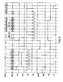
- Figure 4 shows operational timings of the test apparatus 10 according to the embodiment of the present invention.
- the test processing section 110 writes test data into each page of the memory under test 100. Then, the test processing section 110 reads out the written data from each page and compares it with the expectation value.
- Figure 4 shows the operational timings, at which data written into a given page is read out from the memory under test 100 and compared with the expectation value.
- the pattern generator 130 gives a CRL signal having a value "1" to initialize the count value of the counting section 310 (cycle 0).
- the test processing section 110 supplies a "read memory” command to the memory under test 100 based on test pattern data (cycles 1 to 7). To be more specific, the test processing section 110 supplies the command in the cycle 1, a column address in the cycles 2 to 3, and a page address in the cycles 4 to 6, thereby starting reading the memory under test 100.
- the memory under test 100 outputs the data included in the data sequence stored in the designated page, word by word sequentially (cycles x to x+2112).
- the memory under test 100 outputs the data 210 in the correctable area 200 in the cycles x to x+2047, and the error check and correction 220 in the correctable area 200 in the cycles x+2048 to 2050. Since these data can be corrected by the error check and correction, the pattern generator 130 gives an INC signal having a value "1". Thereby, the OR gate 322 and the gate 324 are prohibited from giving notification of a single bit error. Further, the AND gate 315 and the counting section 310 start counting the number of failure bits.
- the classifying section 380 can detect the memory under test 100 as defective, in a case where the count value of the data sequence read out from the correctable area 200 exceeds the upper limit value, which represents the maximum number of errors included in a data sequence that can be corrected by the error check and correction.
- the memory under test 100 outputs the data in the uncorrectable area 230 in the cycles x+2051 to x+2112. Since these data cannot be corrected, the pattern generator 130 gives an INC signal having a value "0". Thereby, the OR gate 322 and the gate 324 are allowed to give notification of a single bit error. Further, the AND gate 315 and the counting section 310 stop counting the number of failure bits. As a result, the classifying section 380 can detect the memory under test 100 as defective, in a case where, for a data sequence read out from the uncorrectable area 230, at least one data included in that data sequence does not match the expectation value.
- the pattern generator 130 gives an LD signal having a value "1".
- the count value of the counting section 310 is supplied to the adder 328 through the OR gates 326-1 to 8.
- the comparing sections 330-1 to 4 compare this count value with the upper limit values stored in the registers 332-1 to 4 respectively.
- the results of this comparison are stored in the BBM 370. Further, based on the results of this comparison, the judging section 334 can judge whether each page of the memory under test 100 meets the condition of each grade.
- the test apparatus 10 can read out the data sequence written into the memory under test 100, and detect the memory under test 100 as defective regarding this data sequence or classify each page of the memory under test 100 into any grade. Then, when defect detection on a given data sequence is completed, the test processing section 110 gives a CLR signal having a value "1" to initialize the count value in the counting section 310. Then, the pattern generator 130 makes the logical comparator 170 start comparison with the expectation value for the next data sequence.
- Figure 5 shows the flow of a process in which the memory under test 100 is tested by the test apparatus 10 according to the embodiment of the present invention and the result thereof is output.
- the test apparatus 10 performs a functionality test for reading out the data sequence stored in each bit of the memory under test 100 and comparing it with the expectation value data sequence (S500). Specifically, first, for each page as the unit of error correction, the test processing section 110 reads out the data sequence stored in that page from the memory under test 100. Then, the logical comparator 170 compares the value of each bit included in the data sequence read out from the memory under test 100 with the expectation value of that bit. Then, based on the result of comparison by the logical comparator 170, the AFM 360 stores bit pass/failure information indicating for each storage cell of the memory under test 100 whether that storage cell is good or defective.
- the counting section 310 and the adder 328 count the number of bits that do not match the expectation value page by page (S510). Then, the page classifying section 340 judges page by page whether the number of bits that do not match the expectation value meets the condition of each of the plurality of grades into which the memory under test 100 is classified based on its quality (S520).
- the output section 380 outputs the bit pass/failure information of each page grade by grade (S530). At this time, in a case where, regarding a given grade and a given page, the number of failures that have occurred in that page meets the condition of that grade, the bit pass/failure information of that page is output as changed to bit pass/failure information obtained in a case where no failure at all has occurred. Then, the repair processing section 190 performs a repair process for replacing defective storage cells with called storage cells, based on the bit pass/failure information of each page output from the output section 380 (S540).
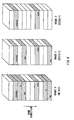
- Figure 6 illustrates an example of a test result output from the test apparatus 10 according to the embodiment of the present invention.
- the steric figures in this drawing represent the aggregation of storage cells in the memory under test 100. Each plane constituting the steric figures represents a page of the memory under test 100.
- the symbol x in the drawing represents the storage cell from which a defect has been detected.
- the grade 0 represents a quality with which normal operability is guaranteed even in a case where no correction by the error check and correction (ECC) is available.
- the grade 1 represents a quality with which normal operability is guaranteed in a case where one bit error can be corrected per page by the error check and correction.
- the grade 2 represents a quality with which normal operability is guaranteed in a case where two bit errors can be corrected per page by the error check and correction.
- the output section 380 just outputs the bit pass/failure information. That is, in this drawing, if there exists one symbol x at all in a given page, this page is judged as defective. On the other hand, at the grade 1, even if there is not more than one defective storage cell in a given page, the page pass/failure information of that page indicates it as good. Hence, for any page that includes only one defective storage cell, the output section 380 does not just output the bit pass/failure information of that page. Instead, the output section 380 outputs bit pass/failure information of the case where no defect has occurred in that page. In the drawing, the third and ninth pages as counted from the top are such pages.
- the page pass/failure information of that page indicates it as good.
- the output section 380 does not just output the bit pass/failure information of that page. Instead, the output section 380 outputs bit pass/failure information of the case where no defect has occurred in that page.
- the third, fourth, ninth, and tenth pages as counted from the top are such pages.
- the output section 380 outputs bit pass/failure information of the case where no defect has occurred in that page, instead of the original bit pass/failure information of that page.
- This enables the repair processing section 190, which uses this output, to acquire only such bit pass/failure information that is about any page that requires a repair process, while omitting a process for analyzing and judging which page requires a repair process.
Landscapes
- Engineering & Computer Science (AREA)
- General Engineering & Computer Science (AREA)
- Physics & Mathematics (AREA)
- General Physics & Mathematics (AREA)
- For Increasing The Reliability Of Semiconductor Memories (AREA)
- Tests Of Electronic Circuits (AREA)
- Diaphragms For Electromechanical Transducers (AREA)
- Maintenance And Management Of Digital Transmission (AREA)
Applications Claiming Priority (2)
| Application Number | Priority Date | Filing Date | Title |
|---|---|---|---|
| JP2006105394 | 2006-04-06 | ||
| PCT/JP2007/055879 WO2007119485A1 (ja) | 2006-04-06 | 2007-03-22 | 試験装置および試験方法 |
Publications (3)
| Publication Number | Publication Date |
|---|---|
| EP2003653A1 true EP2003653A1 (de) | 2008-12-17 |
| EP2003653A4 EP2003653A4 (de) | 2009-10-28 |
| EP2003653B1 EP2003653B1 (de) | 2010-08-04 |
Family
ID=38609270
Family Applications (1)
| Application Number | Title | Priority Date | Filing Date |
|---|---|---|---|
| EP07739322A Not-in-force EP2003653B1 (de) | 2006-04-06 | 2007-03-22 | Testvorrichtung und testverfahren |
Country Status (9)
| Country | Link |
|---|---|
| US (1) | US7984345B2 (de) |
| EP (1) | EP2003653B1 (de) |
| JP (1) | JP4864006B2 (de) |
| KR (2) | KR20090053960A (de) |
| CN (1) | CN101310342A (de) |
| AT (1) | ATE476741T1 (de) |
| DE (1) | DE602007008216D1 (de) |
| TW (1) | TW200739593A (de) |
| WO (1) | WO2007119485A1 (de) |
Families Citing this family (37)
| Publication number | Priority date | Publication date | Assignee | Title |
|---|---|---|---|---|
| JP5029883B2 (ja) * | 2007-05-17 | 2012-09-19 | 横河電機株式会社 | 半導体試験装置 |
| US8234539B2 (en) * | 2007-12-06 | 2012-07-31 | Sandisk Il Ltd. | Correction of errors in a memory array |
| JP2009181600A (ja) * | 2008-01-29 | 2009-08-13 | Renesas Technology Corp | 半導体装置 |
| KR101413137B1 (ko) | 2008-07-04 | 2014-07-01 | 삼성전자주식회사 | 메모리 장치 및 메모리 프로그래밍 방법 |
| JP5038256B2 (ja) * | 2008-08-14 | 2012-10-03 | 株式会社アドバンテスト | 試験モジュールおよび試験方法 |
| US8149730B1 (en) | 2009-05-12 | 2012-04-03 | Juniper Networks, Inc. | Methods and apparatus related to packet generation and analysis |
| US8174991B1 (en) * | 2009-06-29 | 2012-05-08 | Juniper Networks, Inc. | Methods and apparatus related to analysis of test packets |
| JP2011170950A (ja) * | 2010-01-21 | 2011-09-01 | Renesas Electronics Corp | 情報記憶装置及びそのテスト方法 |
| US8258803B2 (en) * | 2010-01-26 | 2012-09-04 | Advantest Corporation | Test apparatus and test method |
| US8201024B2 (en) * | 2010-05-17 | 2012-06-12 | Microsoft Corporation | Managing memory faults |
| JP2012069180A (ja) * | 2010-09-21 | 2012-04-05 | Toshiba Corp | 半導体記憶装置 |
| US8780896B2 (en) | 2010-12-29 | 2014-07-15 | Juniper Networks, Inc. | Methods and apparatus for validation of equal cost multi path (ECMP) paths in a switch fabric system |
| US8798077B2 (en) | 2010-12-29 | 2014-08-05 | Juniper Networks, Inc. | Methods and apparatus for standard protocol validation mechanisms deployed over a switch fabric system |
| TWI459393B (zh) * | 2011-01-19 | 2014-11-01 | Phison Electronics Corp | 用於非揮發性記憶體的資料寫入方法、控制器與儲存裝置 |
| KR101824068B1 (ko) * | 2011-07-28 | 2018-03-15 | 삼성전자주식회사 | 메모리 컨트롤러 구동방법, 및 메모리 컨트롤러를 포함하는 메모리 시스템, 메모리 카드 및 휴대용 전자장치 |
| US8995196B2 (en) | 2011-08-15 | 2015-03-31 | Skymedi Corporation | Method of sorting a multi-bit per cell non-volatile memory and a multi-mode configuration method |
| KR101944793B1 (ko) | 2012-09-04 | 2019-02-08 | 삼성전자주식회사 | 플래시 메모리를 포함하는 플래시 메모리 시스템 및 그것의 비정상 워드 라인 검출 방법 |
| CN102788951B (zh) * | 2012-09-05 | 2015-02-11 | 无锡江南计算技术研究所 | Ate测试结果判断方法及ate测试方法 |
| US9032244B2 (en) | 2012-11-16 | 2015-05-12 | Microsoft Technology Licensing, Llc | Memory segment remapping to address fragmentation |
| US9911509B2 (en) | 2013-12-06 | 2018-03-06 | Intel Corporation | Counter to locate faulty die in a distributed codeword storage system |
| US9600385B2 (en) * | 2014-02-25 | 2017-03-21 | Arrow Devices Pvt Ltd | Analyzing behavior of a device under test |
| CN104979017B (zh) * | 2014-04-03 | 2020-10-27 | 皇虎科技(加拿大)有限公司 | 用于测试及组装存储器模块的系统及方法 |
| US20150363330A1 (en) * | 2014-06-17 | 2015-12-17 | Daniel Robert Watkins | Flash NAND device bad page replacement |
| KR101527690B1 (ko) * | 2014-10-10 | 2015-06-11 | (주) 에이블리 | 낸드 플래시 메모리 테스트 인터페이스 장치 및 그 운용방법 |
| KR102238706B1 (ko) * | 2014-11-28 | 2021-04-09 | 삼성전자주식회사 | 반도체 메모리 장치 및 이를 포함하는 메모리 시스템 |
| KR20160121230A (ko) * | 2015-04-10 | 2016-10-19 | 에스케이하이닉스 주식회사 | 반도체 메모리 장치, 이를 위한 리페어 시스템 및 장치 특성 관리 방법 |
| EP3304820B1 (de) * | 2015-05-27 | 2019-12-18 | Telefonaktiebolaget LM Ericsson (publ) | Verfahren und vorrichtung zur analyse der leistung eines netzwerks durch verwaltung von netzwerkdaten im zusammenhang mit dem betrieb des netzwerks |
| KR20160146332A (ko) * | 2015-06-12 | 2016-12-21 | 에스케이하이닉스 주식회사 | 복수의 저장 영역들을 포함하는 메모리 시스템 및 그것의 동작 방법 |
| CN105139893B (zh) * | 2015-09-27 | 2018-10-16 | 上海华力微电子有限公司 | 一种存储器测试装置及一种存储器芯片测试方法 |
| TWI581093B (zh) | 2016-06-24 | 2017-05-01 | 慧榮科技股份有限公司 | 資料儲存媒體之損壞資料行的篩選方法 |
| KR102545698B1 (ko) * | 2016-09-27 | 2023-06-19 | 삼성전자주식회사 | 데이터 저장 시스템 |
| KR102458563B1 (ko) * | 2018-02-12 | 2022-10-28 | 한국전자통신연구원 | 백스캐터 통신을 사용한 통신 방법 및 통신 장치 |
| KR102507774B1 (ko) * | 2018-03-08 | 2023-03-09 | 에스케이하이닉스 주식회사 | 메모리 칩 및 그것을 포함하는 테스트 시스템 |
| CN113330322B (zh) | 2019-01-22 | 2024-06-21 | 爱德万测试公司 | 使用片上系统测试控制器的自动化测试设备 |
| US11342044B2 (en) * | 2019-05-28 | 2022-05-24 | Nuvoton Technology Corporation | System and method for prioritization of bit error correction attempts |
| KR102790220B1 (ko) * | 2019-07-03 | 2025-04-03 | 에스케이하이닉스 주식회사 | 패일 정보 제어회로, 이를 포함하는 반도체 장치 및 반도체 장치의 패일 정보 제어방법 |
| TWI764297B (zh) * | 2019-11-20 | 2022-05-11 | 大陸商珠海南北極科技有限公司 | 累加電路 |
Family Cites Families (12)
| Publication number | Priority date | Publication date | Assignee | Title |
|---|---|---|---|---|
| KR19990029646A (ko) | 1997-09-09 | 1999-04-26 | 오우라 히로시 | 메모리 시험장치 |
| JP2000173289A (ja) * | 1998-12-10 | 2000-06-23 | Toshiba Corp | エラー訂正可能なフラッシュメモリシステム |
| JP4323707B2 (ja) * | 2000-10-25 | 2009-09-02 | 富士通マイクロエレクトロニクス株式会社 | フラッシュメモリの欠陥管理方法 |
| JP4250325B2 (ja) * | 2000-11-01 | 2009-04-08 | 株式会社東芝 | 半導体記憶装置 |
| DE10297587T5 (de) | 2001-12-18 | 2004-12-02 | Advantest Corp. | Halbleiter-Prüfvorrichtung |
| JP4158526B2 (ja) * | 2003-01-09 | 2008-10-01 | 松下電器産業株式会社 | メモリカード及びメモリへのデータ書き込み方法 |
| JP2005056394A (ja) * | 2003-07-18 | 2005-03-03 | Toshiba Corp | 記憶装置及びメモリカード |
| US7493534B2 (en) * | 2003-08-29 | 2009-02-17 | Hewlett-Packard Development Company, L.P. | Memory error ranking |
| JP4041076B2 (ja) * | 2004-02-27 | 2008-01-30 | 株式会社東芝 | データ記憶システム |
| JP2006012367A (ja) * | 2004-06-29 | 2006-01-12 | Toshiba Corp | 不揮発性半導体記憶装置 |
| JP4261462B2 (ja) * | 2004-11-05 | 2009-04-30 | 株式会社東芝 | 不揮発性メモリシステム |
| US7447955B2 (en) * | 2005-11-30 | 2008-11-04 | Advantest Corporation | Test apparatus and test method |
-
2007
- 2007-03-22 AT AT07739322T patent/ATE476741T1/de not_active IP Right Cessation
- 2007-03-22 DE DE602007008216T patent/DE602007008216D1/de active Active
- 2007-03-22 JP JP2007541563A patent/JP4864006B2/ja not_active Expired - Fee Related
- 2007-03-22 WO PCT/JP2007/055879 patent/WO2007119485A1/ja not_active Ceased
- 2007-03-22 EP EP07739322A patent/EP2003653B1/de not_active Not-in-force
- 2007-03-22 CN CNA200780000113XA patent/CN101310342A/zh active Pending
- 2007-03-22 KR KR1020097007788A patent/KR20090053960A/ko not_active Ceased
- 2007-03-22 KR KR1020077020964A patent/KR20080007544A/ko not_active Ceased
- 2007-03-29 TW TW096110985A patent/TW200739593A/zh unknown
- 2007-09-19 US US11/857,453 patent/US7984345B2/en not_active Expired - Fee Related
Also Published As
| Publication number | Publication date |
|---|---|
| TW200739593A (en) | 2007-10-16 |
| US20080052015A1 (en) | 2008-02-28 |
| KR20080007544A (ko) | 2008-01-22 |
| ATE476741T1 (de) | 2010-08-15 |
| DE602007008216D1 (de) | 2010-09-16 |
| JP4864006B2 (ja) | 2012-01-25 |
| EP2003653B1 (de) | 2010-08-04 |
| JPWO2007119485A1 (ja) | 2009-08-27 |
| KR20090053960A (ko) | 2009-05-28 |
| EP2003653A4 (de) | 2009-10-28 |
| CN101310342A (zh) | 2008-11-19 |
| US7984345B2 (en) | 2011-07-19 |
| WO2007119485A1 (ja) | 2007-10-25 |
Similar Documents
| Publication | Publication Date | Title |
|---|---|---|
| EP2003653B1 (de) | Testvorrichtung und testverfahren | |
| US7634695B2 (en) | Test apparatus and selection apparatus | |
| JP2002538465A (ja) | 単一のテスターチャンネルを使用して複数のデバイスの同時テストを行うための分散型インターフェース | |
| US20080294943A1 (en) | Sata interface tester and testing method | |
| TWI382190B (zh) | 測試裝置及測試方法 | |
| KR101527690B1 (ko) | 낸드 플래시 메모리 테스트 인터페이스 장치 및 그 운용방법 | |
| US7447955B2 (en) | Test apparatus and test method | |
| US5659549A (en) | Memory test system having a pattern generator for a multi-bit test | |
| US7454671B2 (en) | Memory device testing system and method having real time redundancy repair analysis | |
| CN100524538C (zh) | 测试装置与测试方法 | |
| CN114464242A (zh) | 一种ddr测试方法、装置、控制器及存储介质 | |
| US9003251B2 (en) | Diagnosis flow for read-only memories | |
| CN115801540B (zh) | 一种PCIe设备降级检测方法、装置、终端及存储介质 | |
| WO2010018689A1 (ja) | 試験モジュールおよび試験方法 | |
| CN1929034A (zh) | 一种内存故障测试的方法及系统 | |
| CN103137211A (zh) | 一种nvm内建自测电路的仿真测试系统 | |
| WO2006092953A1 (ja) | 試験装置、及び試験方法 | |
| US6850860B2 (en) | Semiconductor device testing apparatus and test method therefor | |
| CN117711475A (zh) | 存储单元的故障检测电路及方法、功能芯片 | |
| CN119556856A (zh) | 固态硬盘数据读取方法、系统、设备及介质 | |
| JPH0997194A (ja) | フェイルメモリのデータ取得装置 | |
| JPH11212731A (ja) | ファイル装置試験方法 | |
| JPH0726785U (ja) | 半導体試験装置用不良解析回路 |
Legal Events
| Date | Code | Title | Description |
|---|---|---|---|
| PUAI | Public reference made under article 153(3) epc to a published international application that has entered the european phase |
Free format text: ORIGINAL CODE: 0009012 |
|
| 17P | Request for examination filed |
Effective date: 20070917 |
|
| AK | Designated contracting states |
Kind code of ref document: A1 Designated state(s): AT BE BG CH CY CZ DE DK EE ES FI FR GB GR HU IE IS IT LI LT LU LV MC MT NL PL PT RO SE SI SK TR |
|
| A4 | Supplementary search report drawn up and despatched |
Effective date: 20090925 |
|
| RIC1 | Information provided on ipc code assigned before grant |
Ipc: G01R 31/28 20060101ALI20090921BHEP Ipc: G11C 29/44 20060101ALI20090921BHEP Ipc: G11C 29/56 20060101AFI20090921BHEP |
|
| GRAP | Despatch of communication of intention to grant a patent |
Free format text: ORIGINAL CODE: EPIDOSNIGR1 |
|
| GRAS | Grant fee paid |
Free format text: ORIGINAL CODE: EPIDOSNIGR3 |
|
| GRAA | (expected) grant |
Free format text: ORIGINAL CODE: 0009210 |
|
| GRAL | Information related to payment of fee for publishing/printing deleted |
Free format text: ORIGINAL CODE: EPIDOSDIGR3 |
|
| GRAS | Grant fee paid |
Free format text: ORIGINAL CODE: EPIDOSNIGR3 |
|
| AK | Designated contracting states |
Kind code of ref document: B1 Designated state(s): AT BE BG CH CY CZ DE DK EE ES FI FR GB GR HU IE IS IT LI LT LU LV MC MT NL PL PT RO SE SI SK TR |
|
| REG | Reference to a national code |
Ref country code: GB Ref legal event code: FG4D |
|
| REG | Reference to a national code |
Ref country code: CH Ref legal event code: EP |
|
| REG | Reference to a national code |
Ref country code: IE Ref legal event code: FG4D |
|
| REF | Corresponds to: |
Ref document number: 602007008216 Country of ref document: DE Date of ref document: 20100916 Kind code of ref document: P |
|
| REG | Reference to a national code |
Ref country code: NL Ref legal event code: VDEP Effective date: 20100804 |
|
| LTIE | Lt: invalidation of european patent or patent extension |
Effective date: 20100804 |
|
| PG25 | Lapsed in a contracting state [announced via postgrant information from national office to epo] |
Ref country code: AT Free format text: LAPSE BECAUSE OF FAILURE TO SUBMIT A TRANSLATION OF THE DESCRIPTION OR TO PAY THE FEE WITHIN THE PRESCRIBED TIME-LIMIT Effective date: 20100804 Ref country code: NL Free format text: LAPSE BECAUSE OF FAILURE TO SUBMIT A TRANSLATION OF THE DESCRIPTION OR TO PAY THE FEE WITHIN THE PRESCRIBED TIME-LIMIT Effective date: 20100804 Ref country code: LT Free format text: LAPSE BECAUSE OF FAILURE TO SUBMIT A TRANSLATION OF THE DESCRIPTION OR TO PAY THE FEE WITHIN THE PRESCRIBED TIME-LIMIT Effective date: 20100804 Ref country code: FI Free format text: LAPSE BECAUSE OF FAILURE TO SUBMIT A TRANSLATION OF THE DESCRIPTION OR TO PAY THE FEE WITHIN THE PRESCRIBED TIME-LIMIT Effective date: 20100804 |
|
| PG25 | Lapsed in a contracting state [announced via postgrant information from national office to epo] |
Ref country code: BG Free format text: LAPSE BECAUSE OF FAILURE TO SUBMIT A TRANSLATION OF THE DESCRIPTION OR TO PAY THE FEE WITHIN THE PRESCRIBED TIME-LIMIT Effective date: 20101104 Ref country code: IS Free format text: LAPSE BECAUSE OF FAILURE TO SUBMIT A TRANSLATION OF THE DESCRIPTION OR TO PAY THE FEE WITHIN THE PRESCRIBED TIME-LIMIT Effective date: 20101204 Ref country code: SI Free format text: LAPSE BECAUSE OF FAILURE TO SUBMIT A TRANSLATION OF THE DESCRIPTION OR TO PAY THE FEE WITHIN THE PRESCRIBED TIME-LIMIT Effective date: 20100804 Ref country code: PT Free format text: LAPSE BECAUSE OF FAILURE TO SUBMIT A TRANSLATION OF THE DESCRIPTION OR TO PAY THE FEE WITHIN THE PRESCRIBED TIME-LIMIT Effective date: 20101206 Ref country code: PL Free format text: LAPSE BECAUSE OF FAILURE TO SUBMIT A TRANSLATION OF THE DESCRIPTION OR TO PAY THE FEE WITHIN THE PRESCRIBED TIME-LIMIT Effective date: 20100804 Ref country code: CY Free format text: LAPSE BECAUSE OF FAILURE TO SUBMIT A TRANSLATION OF THE DESCRIPTION OR TO PAY THE FEE WITHIN THE PRESCRIBED TIME-LIMIT Effective date: 20100804 |
|
| PG25 | Lapsed in a contracting state [announced via postgrant information from national office to epo] |
Ref country code: GR Free format text: LAPSE BECAUSE OF FAILURE TO SUBMIT A TRANSLATION OF THE DESCRIPTION OR TO PAY THE FEE WITHIN THE PRESCRIBED TIME-LIMIT Effective date: 20101105 Ref country code: LV Free format text: LAPSE BECAUSE OF FAILURE TO SUBMIT A TRANSLATION OF THE DESCRIPTION OR TO PAY THE FEE WITHIN THE PRESCRIBED TIME-LIMIT Effective date: 20100804 Ref country code: SE Free format text: LAPSE BECAUSE OF FAILURE TO SUBMIT A TRANSLATION OF THE DESCRIPTION OR TO PAY THE FEE WITHIN THE PRESCRIBED TIME-LIMIT Effective date: 20100804 Ref country code: BE Free format text: LAPSE BECAUSE OF FAILURE TO SUBMIT A TRANSLATION OF THE DESCRIPTION OR TO PAY THE FEE WITHIN THE PRESCRIBED TIME-LIMIT Effective date: 20100804 |
|
| PG25 | Lapsed in a contracting state [announced via postgrant information from national office to epo] |
Ref country code: DK Free format text: LAPSE BECAUSE OF FAILURE TO SUBMIT A TRANSLATION OF THE DESCRIPTION OR TO PAY THE FEE WITHIN THE PRESCRIBED TIME-LIMIT Effective date: 20100804 |
|
| PG25 | Lapsed in a contracting state [announced via postgrant information from national office to epo] |
Ref country code: SK Free format text: LAPSE BECAUSE OF FAILURE TO SUBMIT A TRANSLATION OF THE DESCRIPTION OR TO PAY THE FEE WITHIN THE PRESCRIBED TIME-LIMIT Effective date: 20100804 Ref country code: EE Free format text: LAPSE BECAUSE OF FAILURE TO SUBMIT A TRANSLATION OF THE DESCRIPTION OR TO PAY THE FEE WITHIN THE PRESCRIBED TIME-LIMIT Effective date: 20100804 Ref country code: RO Free format text: LAPSE BECAUSE OF FAILURE TO SUBMIT A TRANSLATION OF THE DESCRIPTION OR TO PAY THE FEE WITHIN THE PRESCRIBED TIME-LIMIT Effective date: 20100804 Ref country code: IT Free format text: LAPSE BECAUSE OF FAILURE TO SUBMIT A TRANSLATION OF THE DESCRIPTION OR TO PAY THE FEE WITHIN THE PRESCRIBED TIME-LIMIT Effective date: 20100804 Ref country code: CZ Free format text: LAPSE BECAUSE OF FAILURE TO SUBMIT A TRANSLATION OF THE DESCRIPTION OR TO PAY THE FEE WITHIN THE PRESCRIBED TIME-LIMIT Effective date: 20100804 |
|
| PLBE | No opposition filed within time limit |
Free format text: ORIGINAL CODE: 0009261 |
|
| STAA | Information on the status of an ep patent application or granted ep patent |
Free format text: STATUS: NO OPPOSITION FILED WITHIN TIME LIMIT |
|
| PG25 | Lapsed in a contracting state [announced via postgrant information from national office to epo] |
Ref country code: ES Free format text: LAPSE BECAUSE OF FAILURE TO SUBMIT A TRANSLATION OF THE DESCRIPTION OR TO PAY THE FEE WITHIN THE PRESCRIBED TIME-LIMIT Effective date: 20101115 |
|
| 26N | No opposition filed |
Effective date: 20110506 |
|
| REG | Reference to a national code |
Ref country code: DE Ref legal event code: R097 Ref document number: 602007008216 Country of ref document: DE Effective date: 20110506 |
|
| PG25 | Lapsed in a contracting state [announced via postgrant information from national office to epo] |
Ref country code: MC Free format text: LAPSE BECAUSE OF NON-PAYMENT OF DUE FEES Effective date: 20110331 |
|
| REG | Reference to a national code |
Ref country code: CH Ref legal event code: PL |
|
| GBPC | Gb: european patent ceased through non-payment of renewal fee |
Effective date: 20110322 |
|
| REG | Reference to a national code |
Ref country code: FR Ref legal event code: ST Effective date: 20111130 |
|
| PG25 | Lapsed in a contracting state [announced via postgrant information from national office to epo] |
Ref country code: MT Free format text: LAPSE BECAUSE OF FAILURE TO SUBMIT A TRANSLATION OF THE DESCRIPTION OR TO PAY THE FEE WITHIN THE PRESCRIBED TIME-LIMIT Effective date: 20100804 |
|
| REG | Reference to a national code |
Ref country code: IE Ref legal event code: MM4A |
|
| PG25 | Lapsed in a contracting state [announced via postgrant information from national office to epo] |
Ref country code: DE Free format text: LAPSE BECAUSE OF NON-PAYMENT OF DUE FEES Effective date: 20111001 Ref country code: IE Free format text: LAPSE BECAUSE OF NON-PAYMENT OF DUE FEES Effective date: 20110322 Ref country code: FR Free format text: LAPSE BECAUSE OF NON-PAYMENT OF DUE FEES Effective date: 20110331 Ref country code: LI Free format text: LAPSE BECAUSE OF NON-PAYMENT OF DUE FEES Effective date: 20110331 Ref country code: CH Free format text: LAPSE BECAUSE OF NON-PAYMENT OF DUE FEES Effective date: 20110331 |
|
| REG | Reference to a national code |
Ref country code: DE Ref legal event code: R119 Ref document number: 602007008216 Country of ref document: DE Effective date: 20111001 |
|
| PG25 | Lapsed in a contracting state [announced via postgrant information from national office to epo] |
Ref country code: GB Free format text: LAPSE BECAUSE OF NON-PAYMENT OF DUE FEES Effective date: 20110322 |
|
| PG25 | Lapsed in a contracting state [announced via postgrant information from national office to epo] |
Ref country code: LU Free format text: LAPSE BECAUSE OF NON-PAYMENT OF DUE FEES Effective date: 20110322 |
|
| PG25 | Lapsed in a contracting state [announced via postgrant information from national office to epo] |
Ref country code: TR Free format text: LAPSE BECAUSE OF FAILURE TO SUBMIT A TRANSLATION OF THE DESCRIPTION OR TO PAY THE FEE WITHIN THE PRESCRIBED TIME-LIMIT Effective date: 20100804 |
|
| PG25 | Lapsed in a contracting state [announced via postgrant information from national office to epo] |
Ref country code: HU Free format text: LAPSE BECAUSE OF FAILURE TO SUBMIT A TRANSLATION OF THE DESCRIPTION OR TO PAY THE FEE WITHIN THE PRESCRIBED TIME-LIMIT Effective date: 20100804 |