EP2003700A2 - Dispositif de conversion photoelectrique et son procede de production - Google Patents
Dispositif de conversion photoelectrique et son procede de production Download PDFInfo
- Publication number
- EP2003700A2 EP2003700A2 EP07740862A EP07740862A EP2003700A2 EP 2003700 A2 EP2003700 A2 EP 2003700A2 EP 07740862 A EP07740862 A EP 07740862A EP 07740862 A EP07740862 A EP 07740862A EP 2003700 A2 EP2003700 A2 EP 2003700A2
- Authority
- EP
- European Patent Office
- Prior art keywords
- layer
- substrate
- photovoltaic
- microcrystalline silicon
- germanium
- Prior art date
- Legal status (The legal status is an assumption and is not a legal conclusion. Google has not performed a legal analysis and makes no representation as to the accuracy of the status listed.)
- Withdrawn
Links
- 238000000034 method Methods 0.000 title claims abstract description 30
- 229910000577 Silicon-germanium Inorganic materials 0.000 claims abstract description 74
- LEVVHYCKPQWKOP-UHFFFAOYSA-N [Si].[Ge] Chemical compound [Si].[Ge] LEVVHYCKPQWKOP-UHFFFAOYSA-N 0.000 claims abstract description 71
- 238000001069 Raman spectroscopy Methods 0.000 claims abstract description 39
- 229910021424 microcrystalline silicon Inorganic materials 0.000 claims abstract description 38
- 239000000758 substrate Substances 0.000 claims description 53
- 239000004065 semiconductor Substances 0.000 claims description 35
- 239000012535 impurity Substances 0.000 claims description 34
- 230000015572 biosynthetic process Effects 0.000 claims description 16
- 229910052732 germanium Inorganic materials 0.000 claims description 16
- GNPVGFCGXDBREM-UHFFFAOYSA-N germanium atom Chemical compound [Ge] GNPVGFCGXDBREM-UHFFFAOYSA-N 0.000 claims description 16
- 238000005259 measurement Methods 0.000 claims description 14
- 238000001228 spectrum Methods 0.000 claims description 14
- 239000007789 gas Substances 0.000 description 37
- 238000000151 deposition Methods 0.000 description 30
- 239000010408 film Substances 0.000 description 28
- 230000008021 deposition Effects 0.000 description 24
- 239000002994 raw material Substances 0.000 description 21
- 238000000623 plasma-assisted chemical vapour deposition Methods 0.000 description 14
- BLRPTPMANUNPDV-UHFFFAOYSA-N Silane Chemical compound [SiH4] BLRPTPMANUNPDV-UHFFFAOYSA-N 0.000 description 13
- 229910021417 amorphous silicon Inorganic materials 0.000 description 13
- 230000000052 comparative effect Effects 0.000 description 12
- 230000000694 effects Effects 0.000 description 8
- QUZPNFFHZPRKJD-UHFFFAOYSA-N germane Chemical compound [GeH4] QUZPNFFHZPRKJD-UHFFFAOYSA-N 0.000 description 8
- 229910052986 germanium hydride Inorganic materials 0.000 description 8
- 239000000463 material Substances 0.000 description 7
- 238000010438 heat treatment Methods 0.000 description 6
- XLOMVQKBTHCTTD-UHFFFAOYSA-N Zinc monoxide Chemical compound [Zn]=O XLOMVQKBTHCTTD-UHFFFAOYSA-N 0.000 description 5
- XOLBLPGZBRYERU-UHFFFAOYSA-N tin dioxide Chemical compound O=[Sn]=O XOLBLPGZBRYERU-UHFFFAOYSA-N 0.000 description 5
- XUIMIQQOPSSXEZ-UHFFFAOYSA-N Silicon Chemical compound [Si] XUIMIQQOPSSXEZ-UHFFFAOYSA-N 0.000 description 4
- 229910052710 silicon Inorganic materials 0.000 description 4
- 239000010703 silicon Substances 0.000 description 4
- HBMJWWWQQXIZIP-UHFFFAOYSA-N silicon carbide Chemical compound [Si+]#[C-] HBMJWWWQQXIZIP-UHFFFAOYSA-N 0.000 description 4
- 238000001237 Raman spectrum Methods 0.000 description 3
- 238000005516 engineering process Methods 0.000 description 3
- 239000005357 flat glass Substances 0.000 description 3
- 238000004519 manufacturing process Methods 0.000 description 3
- 238000003860 storage Methods 0.000 description 3
- 239000013078 crystal Substances 0.000 description 2
- 230000005684 electric field Effects 0.000 description 2
- 229910010271 silicon carbide Inorganic materials 0.000 description 2
- 229920006268 silicone film Polymers 0.000 description 2
- 239000010409 thin film Substances 0.000 description 2
- 239000011787 zinc oxide Substances 0.000 description 2
- LFQSCWFLJHTTHZ-UHFFFAOYSA-N Ethanol Chemical compound CCO LFQSCWFLJHTTHZ-UHFFFAOYSA-N 0.000 description 1
- 229910006160 GeF4 Inorganic materials 0.000 description 1
- 229910007264 Si2H6 Inorganic materials 0.000 description 1
- 229910004014 SiF4 Inorganic materials 0.000 description 1
- BQCADISMDOOEFD-UHFFFAOYSA-N Silver Chemical compound [Ag] BQCADISMDOOEFD-UHFFFAOYSA-N 0.000 description 1
- 238000010521 absorption reaction Methods 0.000 description 1
- 229910052782 aluminium Inorganic materials 0.000 description 1
- XAGFODPZIPBFFR-UHFFFAOYSA-N aluminium Chemical compound [Al] XAGFODPZIPBFFR-UHFFFAOYSA-N 0.000 description 1
- 238000000149 argon plasma sintering Methods 0.000 description 1
- 238000006243 chemical reaction Methods 0.000 description 1
- 238000005229 chemical vapour deposition Methods 0.000 description 1
- 229910021419 crystalline silicon Inorganic materials 0.000 description 1
- 238000002425 crystallisation Methods 0.000 description 1
- 230000008025 crystallization Effects 0.000 description 1
- 238000009792 diffusion process Methods 0.000 description 1
- PZPGRFITIJYNEJ-UHFFFAOYSA-N disilane Chemical compound [SiH3][SiH3] PZPGRFITIJYNEJ-UHFFFAOYSA-N 0.000 description 1
- 230000005611 electricity Effects 0.000 description 1
- 230000005284 excitation Effects 0.000 description 1
- 230000002349 favourable effect Effects 0.000 description 1
- 239000011521 glass Substances 0.000 description 1
- AMGQUBHHOARCQH-UHFFFAOYSA-N indium;oxotin Chemical compound [In].[Sn]=O AMGQUBHHOARCQH-UHFFFAOYSA-N 0.000 description 1
- 229910052751 metal Inorganic materials 0.000 description 1
- 239000002184 metal Substances 0.000 description 1
- 150000002739 metals Chemical class 0.000 description 1
- 238000005457 optimization Methods 0.000 description 1
- ABTOQLMXBSRXSM-UHFFFAOYSA-N silicon tetrafluoride Chemical compound F[Si](F)(F)F ABTOQLMXBSRXSM-UHFFFAOYSA-N 0.000 description 1
- 229910052709 silver Inorganic materials 0.000 description 1
- 239000004332 silver Substances 0.000 description 1
- 238000004611 spectroscopical analysis Methods 0.000 description 1
- 238000004544 sputter deposition Methods 0.000 description 1
- PPMWWXLUCOODDK-UHFFFAOYSA-N tetrafluorogermane Chemical compound F[Ge](F)(F)F PPMWWXLUCOODDK-UHFFFAOYSA-N 0.000 description 1
- 229910001887 tin oxide Inorganic materials 0.000 description 1
- XLYOFNOQVPJJNP-UHFFFAOYSA-N water Substances O XLYOFNOQVPJJNP-UHFFFAOYSA-N 0.000 description 1
Images


Classifications
-
- H—ELECTRICITY
- H10—SEMICONDUCTOR DEVICES; ELECTRIC SOLID-STATE DEVICES NOT OTHERWISE PROVIDED FOR
- H10F—INORGANIC SEMICONDUCTOR DEVICES SENSITIVE TO INFRARED RADIATION, LIGHT, ELECTROMAGNETIC RADIATION OF SHORTER WAVELENGTH OR CORPUSCULAR RADIATION
- H10F77/00—Constructional details of devices covered by this subclass
- H10F77/10—Semiconductor bodies
- H10F77/16—Material structures, e.g. crystalline structures, film structures or crystal plane orientations
- H10F77/162—Non-monocrystalline materials, e.g. semiconductor particles embedded in insulating materials
- H10F77/164—Polycrystalline semiconductors
- H10F77/1642—Polycrystalline semiconductors including only Group IV materials
- H10F77/1648—Polycrystalline semiconductors including only Group IV materials including microcrystalline Group IV-IV materials, e.g. microcrystalline SiGe
-
- H—ELECTRICITY
- H10—SEMICONDUCTOR DEVICES; ELECTRIC SOLID-STATE DEVICES NOT OTHERWISE PROVIDED FOR
- H10F—INORGANIC SEMICONDUCTOR DEVICES SENSITIVE TO INFRARED RADIATION, LIGHT, ELECTROMAGNETIC RADIATION OF SHORTER WAVELENGTH OR CORPUSCULAR RADIATION
- H10F71/00—Manufacture or treatment of devices covered by this subclass
- H10F71/121—The active layers comprising only Group IV materials
- H10F71/1215—The active layers comprising only Group IV materials comprising at least two Group IV elements, e.g. SiGe
- H10F71/1218—The active layers comprising only Group IV materials comprising at least two Group IV elements, e.g. SiGe in microcrystalline form
-
- Y—GENERAL TAGGING OF NEW TECHNOLOGICAL DEVELOPMENTS; GENERAL TAGGING OF CROSS-SECTIONAL TECHNOLOGIES SPANNING OVER SEVERAL SECTIONS OF THE IPC; TECHNICAL SUBJECTS COVERED BY FORMER USPC CROSS-REFERENCE ART COLLECTIONS [XRACs] AND DIGESTS
- Y02—TECHNOLOGIES OR APPLICATIONS FOR MITIGATION OR ADAPTATION AGAINST CLIMATE CHANGE
- Y02E—REDUCTION OF GREENHOUSE GAS [GHG] EMISSIONS, RELATED TO ENERGY GENERATION, TRANSMISSION OR DISTRIBUTION
- Y02E10/00—Energy generation through renewable energy sources
- Y02E10/50—Photovoltaic [PV] energy
- Y02E10/547—Monocrystalline silicon PV cells
-
- Y—GENERAL TAGGING OF NEW TECHNOLOGICAL DEVELOPMENTS; GENERAL TAGGING OF CROSS-SECTIONAL TECHNOLOGIES SPANNING OVER SEVERAL SECTIONS OF THE IPC; TECHNICAL SUBJECTS COVERED BY FORMER USPC CROSS-REFERENCE ART COLLECTIONS [XRACs] AND DIGESTS
- Y02—TECHNOLOGIES OR APPLICATIONS FOR MITIGATION OR ADAPTATION AGAINST CLIMATE CHANGE
- Y02E—REDUCTION OF GREENHOUSE GAS [GHG] EMISSIONS, RELATED TO ENERGY GENERATION, TRANSMISSION OR DISTRIBUTION
- Y02E10/00—Energy generation through renewable energy sources
- Y02E10/50—Photovoltaic [PV] energy
- Y02E10/548—Amorphous silicon PV cells
Definitions
- the present invention relates to a photovoltaic device having microcrystalline silicon-germanium as an i-layer of a photovoltaic layer, and a process for producing the same.
- a photovoltaic device that converts the energy from sunlight into electrical energy is a thin-film silicon-based photovoltaic device in which the photovoltaic layer is formed by deposition using a plasma enhanced CVD method.
- One potential candidate for the photovoltaic layer film used in a thin-film silicon-based photovoltaic device is a microcrystalline silicon-germanium film. Because microcrystalline silicon-germanium films have a narrower gap than microcrystalline silicon and also exhibit excellent absorption properties, they hold considerable potential as photovoltaic materials capable of absorbing the long wavelength region of sunlight and thus improving the conversion efficiency by including these films in laminated structures with other photovoltaic materials such as amorphous silicon or microcrystalline silicon.
- the largest portion of the photovoltaic layer is generally formed from an i-layer composed of an intrinsic semiconductor, and a structure is usually employed in which this i-layer is sandwiched between a thin p-layer formed from a semiconductor doped with a p-type impurity, and a thin n-layer formed from a semiconductor doped with an n-type impurity.
- Patent Citation 1 Publication of Japanese Patent No. 3,684,041 (paragraph [0021] and FIG. 1 )
- the present invention has been developed in light of the above circumstances, and has an object of providing a photovoltaic device with improved cell properties having a photovoltaic layer comprising microcrystalline silicon-germanium, as well as a process for producing the device.
- microcrystalline silicon-germanium used in the photovoltaic layer differs from amorphous silicon-germanium, and the crystallinity has an effect on the cell properties.
- the electrical properties of the resulting device structure were considered, but until now, no technique has been proposed that also considers the crystal growth of the microcrystalline silicon-germanium.
- the inventors of the present invention focused their attention on the film quality of the buffer layer, not only in terms of its effect on the electrical properties of the device structure, but also in terms of its the role as a base layer during crystal growth of the microcrystalline silicon-germanium of the i-layer, and they were therefore able to complete the present invention.
- the photovoltaic device of the present invention is a photovoltaic device having a substrate and a photovoltaic layer provided on top of the substrate, the photovoltaic layer including a p-layer comprising a semiconductor doped with a p-type impurity, an n-layer comprising a semiconductor doped with an n-type impurity, and an i-layer comprising mainly microcrystalline silicon-germanium that is provided between the p-layer and the n-layer, wherein a buffer layer comprising mainly microcrystalline silicon or microcrystalline silicon-germanium is disposed between the substrate-side impurity-doped layer, which is the layer among the p-layer and the n-layer positioned closer to the substrate, and the above i-layer, and the Raman peak ratio Ic(1)/Ia(1) (480 cm -1 ) for the buffer layer, which represents the ratio within a Raman spectroscopic measurement spectrum of the peak intensity Ic(1) of the crystalline phase relative to the peak intensity Ia
- a ratio of 0.8 or greater means that the buffer layer comprises an essentially crystalline layer.
- the p-layer and n-layer may be microcrystalline silicon, microcrystalline SiGe or microcrystalline SiC.
- the buffer layer provided on the substrate-side of the i-layer has a high degree of crystallinity, the film quality of the microcrystalline silicon-germanium within the i-layer is improved, thereby improving the cell properties.
- the photovoltaic device of the present invention may be a photovoltaic device having a substrate and a photovoltaic layer provided on top of the substrate, the photovoltaic layer including a p-layer comprising a semiconductor doped with a p-type impurity, an n-layer comprising a semiconductor doped with an n-type impurity, and an i-layer comprising mainly microcrystalline silicon-germanium that is provided between the p-layer and the n-layer, wherein a Raman peak ratio Ic(2)/Ia(2) for the substrate-side impurity-doped layer, which is the layer among the p-layer and the n-layer that is positioned closer to the substrate, is not less than 2, in which the Raman peak ratio Ic(2)/Ia(2) represents the ratio within a Raman spectroscopic measurement spectrum of a peak intensity Ic(2) of a crystalline phase relative to a peak intensity Ia(2) of an amorphous phase.
- Providing a buffer layer comprising mainly microcrystalline silicon or microcrystalline silicon-germanium between the substrate-side impurity-doped layer and the i-layer is preferred, as it enables the degree of improvement in the cell properties to be further enhanced.
- the germanium concentration within the buffer layer is preferably lower than the germanium concentration within the i-layer.
- a process for producing a photovoltaic device is a process comprising the formation of a photovoltaic layer on top of a substrate, the formation of the photovoltaic layer comprising the steps of: forming a p-layer comprising a semiconductor doped with a p-type impurity, an i-layer comprising mainly microcrystalline silicon-germanium, and an n-layer comprising a semiconductor doped with an n-type impurity, either in that sequence or in a reverse sequence, and further comprising a step of forming a buffer layer comprising mainly microcrystalline silicon or microcrystalline silicon-germanium, which is performed between the step of forming the substrate-side impurity-doped layer, which is the layer among the p-layer and the n-layer positioned closer to the substrate, and the step of forming the i-layer, wherein the Raman peak ratio Ic(1)/Ia(1) for the buffer layer, which represents the ratio within a Raman spectroscopic measurement spectrum of the peak
- the p-layer and n-layer may be microcrystalline silicon, microcrystalline SiGe or microcrystalline SiC. Furthermore, layers comprising mainly microcrystalline silicon or microcrystalline silicon-germanium may be formed in advance under a variety of conditions in order to enable setting of the conditions, and the conditions that result in a Raman peak ratio Ic(1)/Ia(1) for this layer, namely a ratio within the Raman spectroscopic measurement spectrum of the peak intensity Ic(1) of the crystalline phase relative to the peak intensity Ia(1) of the amorphous phase, of not less than 0.8 may then be selected and used as the basis for formation of the buffer layer.
- the film quality of the microcrystalline silicon-germanium within the i-layer improves, enabling production of a photovoltaic device with improved cell properties.
- the process for producing a photovoltaic device may be a process comprising the formation of a photovoltaic layer on top of a substrate, the formation of the photovoltaic layer comprising the steps of: forming a p-layer comprising a semiconductor doped with a p-type impurity, an i-layer comprising mainly microcrystalline silicon-germanium, and an n-layer comprising a semiconductor doped with an n-type impurity, either in that sequence or in a reverse sequence, wherein in the step of forming the substrate-side impurity-doped layer, which is the layer among the p-layer and the n-layer positioned closer to the substrate, the Raman peak ratio Ic(2)/Ia(2) of the substrate-side impurity-doped layer, which represents the ratio within a Raman spectroscopic measurement spectrum of the peak intensity Ic(2) of the crystalline phase relative to the peak intensity Ia(2) (480 cm -1 ) of the amorphous phase,
- impurity-doped layers may be formed in advance under a variety of conditions in order to enable setting of the conditions, and the conditions that result in a Raman peak ratio Ic(2)/Ia(2) for this layer, namely a ratio within the Raman spectroscopic measurement spectrum of the peak intensity Ic(2) of the crystalline phase relative to the peak intensity Ia(2) of the amorphous phase, of not less than 2 may then be selected and used as the basis for formation of the impurity-doped layer of the photovoltaic device.
- the film quality of the microcrystalline silicon-germanium within the i-layer improves, enabling production of a photovoltaic device with improved cell properties.
- Providing a step of forming a buffer layer comprising mainly microcrystalline silicon or microcrystalline silicon-germanium between the step of forming the substrate-side impurity-doped layer and the step of forming the i-layer is preferred, as it enables the degree of improvement in the cell properties to be further enhanced.
- the germanium concentration within the buffer layer is preferably lower than the germanium concentration within the i-layer.
- the present invention is able to provide a photovoltaic device with improved cell properties having a photovoltaic layer comprising microcrystalline silicon-germanium, as well as a process for producing the device.
- This embodiment provides a description of a so-called single type photovoltaic layer, having a p-layer composed of a semiconductor doped with a p-type impurity and an n-layer composed of a semiconductor doped with an n-type impurity formed on the top and bottom of an i-layer composed of an intrinsic semiconductor.
- the description focuses on a photovoltaic device with a substrate-side illuminated PIN structure, but the technology could be expected to yield similar effects in a NIP structure or film-side illuminated photovoltaic device.
- FIG. 1 is a schematic sectional view showing a photovoltaic device according to the first embodiment.
- This photovoltaic device comprises a substrate 1, a first transparent electrode 2, a photovoltaic layer 3, a second transparent electrode 9, and a back electrode 10.
- the substrate 1 is a transparent, electrically insulating substrate onto which the photovoltaic layer 3 and the various electrodes are deposited.
- the substrate 1 is exemplified by a thin sheet of white sheet glass.
- the first transparent electrode 2 is the electrode on the sunlight-incident side of the photovoltaic device, and is exemplified by a transparent conductive oxide material such as tin oxide (SnO 2 ) or zinc oxide (ZnO).
- the photovoltaic layer 3 is a layer that converts light into electricity.
- FIG. 2 shows an enlarged sectional view of the photovoltaic layer 3.
- the photovoltaic layer 3 comprises a p-layer 4, an i-layer 5, and an n-layer 6.
- the p-layer 4 is a semiconductor layer that has been doped with a p-type impurity.
- the p-layer 4 is exemplified by a p-type microcrystalline silicon.
- the i-layer 5 is a semiconductor layer that has not been intentionally doped with an impurity.
- the i-layer 5 comprises microcrystalline silicon-germanium.
- the n-layer 6 is a semiconductor layer that has been doped with an n-type impurity.
- the n-layer 6 is exemplified by an n-type microcrystalline silicon.
- a first buffer layer 51 is formed between the p-layer 4 and the i-layer 5.
- the first buffer layer 51 is a buffer layer comprising mainly microcrystalline silicon or microcrystalline silicon-germanium, and the Raman peak ratio Ic(1)/Ia(1) for the buffer layer, which represents the ratio within a Raman spectroscopic measurement spectrum of the peak intensity Ic(1) of the crystalline phase relative to the peak intensity Ia(1) (480 cm -1 ) of the amorphous phase, is specified as being not less than 0.8.
- a peak shift occurs in the case of microcrystalline SiGe, the peak intensity attributable to a crystalline Si layer can be used as Ic, and the intensity at 480 cm -1 can be used as Ia.
- the Raman peak ratio is an indicator of the crystallization ratio, and is measured as follows. First, a measuring light is irradiated onto the film surface of the first buffer layer 51. Monochromatic laser light is used as the measuring light, and the use of frequency-doubled YAG laser light (wavelength: 532 nm) is ideal. When the measuring light is irradiated from the film surface side of the first buffer layer, Raman scattering is observed. In the Raman spectrum obtained by spectroscopic analysis of the emitted Raman scattered light, a Raman peak ratio Ic(1)/Ia(1) that represents the ratio of the peak intensity Ic(1) of the crystalline phase relative to the peak intensity Ia(1) of the amorphous phase can be determined.
- the "peak intensity of the amorphous phase” typically refers to the peak intensity near a frequency of 480 cm -1
- peak intensity of the crystalline phase typically refers to the peak intensity near a frequency of 520 cm -1 .
- the germanium concentration within the first buffer layer is preferably lower than the germanium concentration within the i-layer 5.
- a second buffer layer 52 may be provided between the i-layer 5 and the n-layer 6.
- This second buffer layer 52 differs from the first buffer layer 51, and there are no particular restrictions regarding its crystallinity.
- materials that can be used as the second buffer layer 52 include microcrystalline silicon, microcrystalline silicon-germanium, amorphous silicon and amorphous silicon-germanium.
- another layer may be inserted between the first transparent electrode 2 and the photovoltaic layer 3.
- layers include a layer that improves the crystallinity of the upper layer, and a layer that prevents the diffusion of impurities from other layers.
- the second transparent electrode 9 and the back electrode 10 represent the electrodes on the back side of the photovoltaic device.
- the second transparent electrode 9 is exemplified by transparent conductive oxide materials such as ZnO or indium tin oxide (ITO).
- the back electrode 10 is exemplified by high reflectance metals such as silver (Ag) and aluminum (A1).
- Another layer (such as a layer that improves the reflectance or light scattering of the second transparent electrode 9) may be inserted between the second transparent electrode 9 and the photovoltaic layer 3.
- FIG. 3 is a schematic view showing an example of a plasma enhanced CVD apparatus used for producing the photovoltaic device of this embodiment.
- the plasma enhanced CVD apparatus 20 comprises a vacuum chamber 11, a high frequency power source 17, a gas supply unit 18, and although not shown in the figure, a turbomolecular pump and rotary pump for vacuum evacuation of the vacuum chamber, and a dry pump (not shown) for exhausting the raw material gases.
- a different plasma enhanced CVD apparatus is provided for film deposition of each of the p-, i- and n-layers, and these plasma enhanced CVD apparatuses are arranged so that the substrate can be transported under vacuum from one apparatus to the next via a transport chamber.
- the ultra high frequency power source 17 supplies high frequency electrical power with desired properties (for example, a plasma excitation frequency of 60 to 120 MHz) to the discharge electrode (described below) inside the vacuum chamber 11.
- the gas supply unit 18 supplies a raw material gas 19 at a predetermined flow rate or flow rate ratio from a gas storage unit 16 to the vacuum chamber 11 via a gas flow rate controller 15.
- the gas storage unit 16 is exemplified by a plurality of gas cylinders containing different gases.
- the gas flow rate controller 15 is exemplified by mass flow meters provided for each of the plurality of gas cylinders.
- the supplied high frequency electrical power and the supplied gas or plurality of gases enable films that form each of the layers of the photovoltaic device to be deposited on top of the substrate 1.
- the vacuum chamber 11 comprises a first electrode 12, a second electrode 13, and a raw material gas supply unit 14.
- the first electrode 12 incorporates a heater function for heating the substrate, and also supports and grounds the substrate 1.
- the second electrode 13 is supplied with the desired level of electrical power from the high frequency power source 17, and generates a plasma of the supplied raw material gas 19 between the second electrode 13 and the first electrode 12.
- the second electrode 13 is separated from the substrate 1 by a predetermined gap length dg, and opposes the first electrode 12. In this embodiment, parallel plate electrodes are used, but there are no particular restrictions on the electrode shape.
- the raw material gas supply unit 14 introduces the raw material gas 19 into the space where the plasma is formed (the space between the first electrode 12 and the second electrode 13) via the gaps within the second electrode 13.
- the second electrode 13 and the raw material gas supply unit 14 may be integrated, so that one of the components incorporates the function of the other.
- a process for producing the photovoltaic device is described below.
- the production conditions described below merely represent a single example, and the present invention is not limited to these conditions.
- a base material is prepared by using a heated CVD method to form a film of SnO 2 as the first transparent electrode 2 on the surface of a white sheet glass substrate as the substrate 1, and this base material is then washed with pure water or alcohol.
- a film that is required for ensuring favorable growth of the SnO 2 , or a refractive index adjustment film that lowers the reflectance may be inserted between the white sheet glass and the SnO 2 .
- the substrate 1 is installed inside a plasma enhanced CVD apparatus used for p-layer deposition, and a p-type microcrystalline silicone film that functions as the p-layer 4 of the photovoltaic layer 3 is deposited by plasma enhanced CVD on the surface of the first transparent electrode 2 formed on top of the substrate 1.
- the deposition conditions involve vacuum evacuation of the chamber 11 to a pressure of not more than 10 -4 Pa, and then heating of the substrate 1 to 150°C.
- the raw material gases SiH 4 , H 2 , and B 2 H 6 which acts as the p-type impurity gas, are then introduced into the vacuum chamber 11 at flow rates of 3, 300 and 0.02 sccm respectively, and the pressure is controlled at 67 Pa.
- the gap length dg is 25 mm.
- a plasma is generated between the second electrode 13 and the substrate 1, thereby depositing a p-type microcrystalline silicon layer of 20 nm as the p-layer 4 on top of the first transparent electrode 2.
- an i-type microcrystalline silicon film that functions as the first buffer layer 51 is deposited by plasma enhanced CVD on top of the p-layer 4.
- Deposition of the first buffer layer 51 may be performed in either the p-layer deposition chamber or the i-layer deposition chamber, or may, of course, also be performed in a dedicated buffer layer deposition chamber.
- the deposition conditions involve vacuum evacuation of the chamber 11 to a pressure of not more than 10 -4 Pa, and then heating of the substrate 1 to 200°C.
- the raw material gases SiH 4 and H 2 are then introduced into the vacuum chamber 11 at flow rates of 0.5 SLM/m 2 and 15 SLM/m 2 respectively, and the pressure is controlled at 266 Pa.
- the gap length dg is 5 mm.
- a plasma is generated between the second electrode 13 and the substrate 1, thereby depositing a microcrystalline silicon layer as the first buffer layer 51 on top of the p-layer 4.
- a first buffer layer 51 comprising microcrystalline silicon-germanium can be deposited.
- a first buffer layer 51 can be formed with a profile in which the Ge concentration increases from the p-layer 4 through to the i-layer 5.
- the crystallinity of the first buffer layer can be controlled by adjusting the ratio H 2 /SiH 4 or the ratio H 2 /(SiH 4 +GeH 4 ). Furthermore, the crystallinity also changes with variations in the electrical power level, the pressure and the gap length, and the crystallinity may also be controlled by selecting suitable values for the ratio H 2 /SiH 4 or the ratio H 2 /(SiH 4 +GeH 4 ) at the conditions chosen.
- the conditions required for controlling the crystallinity of the first buffer layer can be set by first depositing layers comprising mainly microcrystalline silicon or microcrystalline silicon-germanium (for example, with a film thickness of approximately 500 nm) as condition-setting samples under a variety of conditions, and then selecting the deposition conditions that yield the desired crystallinity. Deposition can then be performed for the actual photovoltaic device based on these selected crystallinity control conditions.
- a microcrystalline silicon-germanium film that functions as the i-layer 5 is deposited by plasma enhanced CVD on top of the first buffer layer 51.
- the deposition conditions involve vacuum evacuation of the chamber 11 to a pressure of not more than 10 -4 Pa, and then heating of the substrate 1 to 200°C.
- the raw material gases are then introduced into the vacuum chamber 11, and the pressure is controlled at 267 Pa.
- a raw material gas for silicon and a raw material gas for germanium are used as the raw material gases.
- the raw material gas for silicon comprises at least one of SiH 4 , Si 2 H 6 and SiF 4 .
- the raw material gas for germanium comprises at least one of GeH 4 and GeF 4 .
- the gap length dg is 5 mm.
- a plasma is generated between the second electrode 13 and the substrate 1, thereby depositing a microcrystalline silicon-germanium layer of 1000nm as the i-layer 5 on top of the first buffer layer 51.
- a second buffer layer 52 may be deposited by plasma enhanced CVD on top of the i-layer 5.
- Deposition of the second buffer layer 52 may be performed in either the n-layer deposition chamber or the i-layer deposition chamber, or may, of course, also be performed in a dedicated buffer layer deposition chamber.
- the second buffer layer 52 may be deposited, for example, using the same method as that described for the first buffer layer 51. Namely, an i-type microcrystalline silicon film that functions as the second buffer layer 52 may be deposited by plasma enhanced CVD on top of the i-layer 5.
- Deposition of the second buffer layer 52 may be performed in either the i-layer deposition chamber or the n-layer deposition chamber, or may, of course, also be performed in a dedicated buffer layer deposition chamber.
- the deposition conditions involve vacuum evacuation of the chamber 11 to a pressure of not more than 10 -4 Pa, and then heating of the substrate 1 to 200°C.
- the raw material gases SiH 4 and H 2 are then introduced into the vacuum chamber 11 at flow rates of 0.8 SLM/m 2 and 15 SLM/m 2 respectively, and the pressure is controlled at 266 Pa.
- the gap length dg is 5 mm.
- a plasma is generated between the second electrode 13 and the substrate 1, thereby depositing a microcrystalline silicon layer as the second buffer layer 52 on top of the i-layer 5.
- a second buffer layer 52 comprising microcrystalline silicon-germanium can be deposited.
- a second buffer layer 52 can be formed with a profile in which the Ge concentration increases from the p-layer 4 through to the i-layer 5.
- the crystallinity of the second buffer layer can be controlled by adjusting the ratio H 2 /SiH 4 or the ratio H 2 / (SiH 4 +GeH 4 ).
- an n-type microcrystalline silicone film that functions as the n-layer 6 is deposited by plasma enhanced CVD on the surface of the second buffer layer 52 or the i-layer 5.
- the deposition conditions involve vacuum evacuation of the chamber 11 to a pressure of not more than 10 -4 Pa, and then heating of the substrate 1 to 170°C.
- the raw material gases SiH 4 , H 2 , and PH 3 which acts as the n-type impurity gas, are then introduced into the vacuum chamber 11 at flow rates of 3, 300 and 0.1 sccm respectively, and the pressure is controlled at 93 Pa.
- the gap length dg is 25 mm.
- a plasma is generated between the second electrode 13 and the substrate 1, thereby depositing an n-type microcrystalline silicon layer of 30 nm as the n-layer 6 on top of the second buffer layer 52.
- sputtering is used to deposit a ZnO film of 80 nm as the second transparent electrode 9 on top of the n-layer 6, and then an Ag film of 300 nm as the back electrode 10 on top of the second transparent electrode 9.
- the deposition conditions may employ conventional conditions.
- a photovoltaic device is formed that includes microcrystalline silicon-germanium as the i-layer of the photovoltaic layer 3.
- the photovoltaic device of the first embodiment shown in FIG. 1 and FIG. 2 was fabricated under two different sets of deposition conditions, and the resulting devices were termed example 1 and example 2 respectively.
- the first buffer layer was a microcrystalline silicon layer in both the example 1 and the example 2.
- the Raman peak ratio Ic(1)/Ia(1) that indicates the crystallinity of the first buffer layer 51 was 3.7 and 9.5 respectively.
- the Raman peak ratio that indicates the crystallinity of the buffer layer was calculated as the ratio between the intensity Ic of the peak attributable to the crystalline phase (approximately 520 cm -1 ) and the intensity Ia of the peak attributable to the amorphous phase (480 cm -1 ) within the Raman spectrum for a film of 500 nm deposited on a glass substrate.
- the Raman spectrum was measured using a microscopic Raman spectrometer, using frequency-doubled YAG laser light of 532 nm as the light source.
- a photovoltaic device that contained no first buffer layer 51, and a photovoltaic device in which the first buffer layer 51 was replaced with an amorphous silicon layer were produced as a comparative example 1 and a comparative example 2 respectively.
- FIG. 4 through FIG. 7 are graphs showing the relationships between the crystallinity of the first buffer layer and the cell properties, wherein FIG. 4 shows the short-circuit current density Jsc, FIG. 5 shows the open-circuit voltage Voc, FIG. 6 shows the fill factor FF, and FIG. 7 shows the cell efficiency.
- the value for the particular cell property is expressed as a relative value, wherein the value for the comparative example 1 (which contains no first buffer layer) is deemed to be 1. The results are omitted for the comparative example 1.
- the amorphous silicon layer used as the first buffer layer 51 has an effect on the crystallinity of the microcrystalline silicon-germanium that constitutes the i-layer 5, causing a dramatic reduction in the crystallinity of the i-layer 5. Accordingly, it is evident that in photovoltaic devices comprising microcrystalline silicon-germanium as the i-layer 5, the introduction of a buffer layer does not necessarily result in improved cell properties.
- the short-circuit current density Jsc improves markedly, and the cell efficiency compared with that of the comparative example 1, increases approximately 30% for the example 1 and approximately 55% for the example 2.
- using a microcrystalline silicon with a high degree of crystallinity as the first buffer layer 51 also improves the film quality of the microcrystalline silicon-germanium of the i-layer 5. As a result, the cell efficiency of the photovoltaic device improves.
- the germanium concentration within the first buffer layer 51 is set to a lower value than the germanium concentration in the microcrystalline silicon-germanium of the i-layer 5.
- This embodiment provides a description of a so-called tandem type photovoltaic layer having two photovoltaic layers, wherein each photovoltaic layer comprises a p-layer composed of a semiconductor doped with a p-type impurity and an n-layer composed of a semiconductor doped with an n-type impurity formed on the top and bottom of an i-layer composed of an intrinsic semiconductor.
- the description focuses on a photovoltaic device with a substrate-side illuminated PIN structure, but the technology could be expected to yield similar effects in a NIP structure or film-side illuminated photovoltaic device.
- FIG. 8 is a schematic partial sectional view showing a photovoltaic device according to the second embodiment.
- This photovoltaic device comprises a substrate 1, a first transparent electrode 2, a first photovoltaic layer (a top cell) 31, a second photovoltaic layer (a bottom cell) 33, a second transparent electrode 9, and a back electrode 10.
- the substrate 1, the first transparent electrode 2, the second transparent electrode 9 and the back electrode 10 are the same as those described for the first embodiment, and therefore their descriptions are omitted here.
- the second photovoltaic layer (the bottom cell) 33 has the same configuration as the photovoltaic layer 3 of the first embodiment, and therefore its description is also omitted.
- the first photovoltaic layer (the top cell) 31 may employ amorphous silicon, microcrystalline silicon, amorphous silicon-germanium or microcrystalline silicon carbide or the like.
- the second photovoltaic layer 33 has the same configuration as the photovoltaic layer 3 of the first embodiment, microcrystalline silicon with a high degree of crystallinity is used as the first buffer layer within the second photovoltaic layer 33, thereby improving the film quality of the microcrystalline silicon-germanium of the i-layer. As a result, the cell efficiency of the photovoltaic device also improves.
- This embodiment provides a description of a so-called triple type photovoltaic layer having three photovoltaic layers, wherein each photovoltaic layer comprises a p-layer composed of a semiconductor doped with a p-type impurity and an n-layer composed of a semiconductor doped with an n-type impurity formed on the top and bottom of an i-layer composed of an intrinsic semiconductor.
- the description focuses on a photovoltaic device with a substrate-side illuminated PIN structure, but the technology could be expected to yield similar effects in a NIP structure or film-side illuminated photovoltaic device.
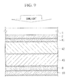
- FIG. 9 is a schematic partial sectional view showing a photovoltaic device according to the third embodiment.
- This photovoltaic device comprises a substrate 1, a first transparent electrode 2, a first photovoltaic layer (a top cell) 41, a second photovoltaic layer (a middle cell) 42, a third photovoltaic layer (a bottom cell) 43, a second transparent electrode 9, and a back electrode 10.
- the substrate 1, the first transparent electrode 2, the second transparent electrode 9 and the back electrode 10 are the same as those described for the first embodiment, and therefore their descriptions are omitted here.
- the third photovoltaic layer (the bottom cell) 43 has the same configuration as the photovoltaic layer 3 of the first embodiment, and therefore its description is also omitted.
- Amorphous silicon is employed for the first photovoltaic layer (the top cell) 41, and microcrystalline silicon is employed for the second photovoltaic layer.
- Examples of other configurations that may be employed for the combination of the first photovoltaic layer / second photovoltaic layer/ third photovoltaic layer include, besides the combination described above, amorphous silicon / amorphous silicon / microcrystalline silicon-germanium, amorphous silicon / amorphous silicon-germanium /microcrystalline silicon-germanium, and microcrystalline silicon carbide / amorphous silicon / microcrystalline silicon-germanium.
- the third photovoltaic layer 43 has the same configuration as the photovoltaic layer 3 of the first embodiment, microcrystalline silicon with a high degree of crystallinity is used as the first buffer layer within the third photovoltaic layer 43, thereby improving the film quality of the microcrystalline silicon-germanium of the i-layer. As a result, the cell efficiency of the photovoltaic device also improves.
- the cell efficiency of the photovoltaic layer comprising microcrystalline silicon-germanium as the i-layer was improved by improving the crystallinity of the first buffer layer 51, but in this embodiment, the crystallinity of the p-layer 4 is improved without providing a first buffer layer 51.
- the p-layer 4 comprises mainly microcrystalline silicon or microcrystalline silicon-germanium, and has a Raman peak ratio Ic(2)/Ia(2), which represents the ratio within a Raman spectroscopic measurement spectrum of the peak intensity Ic(2) of the crystalline phase relative to the peak intensity Ia(2) of the amorphous phase, that is specified as being not less than 2, and preferably not less than 4.
- the method used for measuring the Raman peak ratio for the p-layer 4 is the same as that used for measuring the first buffer layer 51 in the first embodiment, and a description of the method is therefore omitted here.
- the crystallinity and film quality of the i-layer 5 composed of microcrystalline silicon-germanium also improves, yielding improved cell properties.
- providing a buffer layer between the p-layer 4 of improved crystallinity and the i-layer 5 composed of microcrystalline silicon-germanium is preferred, as it enables the degree of improvement in the cell properties to be further enhanced.
- Microcrystalline silicon or microcrystalline silicon-germanium can be used as this buffer layer.
- the germanium concentration within the first buffer layer is preferably lower than the germanium concentration within the i-layer 5.
Landscapes
- Photovoltaic Devices (AREA)
Applications Claiming Priority (2)
| Application Number | Priority Date | Filing Date | Title |
|---|---|---|---|
| JP2006102162A JP2007281018A (ja) | 2006-04-03 | 2006-04-03 | 光電変換装置及びその製造方法 |
| PCT/JP2007/057426 WO2007114432A1 (fr) | 2006-04-03 | 2007-04-03 | Dispositif de conversion photoelectrique et son procede de production |
Publications (2)
| Publication Number | Publication Date |
|---|---|
| EP2003700A2 true EP2003700A2 (fr) | 2008-12-17 |
| EP2003700A9 EP2003700A9 (fr) | 2009-05-06 |
Family
ID=38563696
Family Applications (1)
| Application Number | Title | Priority Date | Filing Date |
|---|---|---|---|
| EP07740862A Withdrawn EP2003700A2 (fr) | 2006-04-03 | 2007-04-03 | Dispositif de conversion photoelectrique et son procede de production |
Country Status (6)
| Country | Link |
|---|---|
| US (1) | US20100163100A1 (fr) |
| EP (1) | EP2003700A2 (fr) |
| JP (1) | JP2007281018A (fr) |
| CN (2) | CN101395721B (fr) |
| AU (1) | AU2007232806A1 (fr) |
| WO (1) | WO2007114432A1 (fr) |
Cited By (3)
| Publication number | Priority date | Publication date | Assignee | Title |
|---|---|---|---|---|
| EP2273564A3 (fr) * | 2009-07-03 | 2012-12-19 | Kisco | Dispositif photovoltaïque et son procédé de fabrication |
| EP2262005A3 (fr) * | 2009-06-12 | 2013-01-23 | Kisco | Dispositif photovoltaïque et son procédé de fabrication |
| US10998459B2 (en) | 2016-07-29 | 2021-05-04 | Exeger Operations Ab | Light absorbing layer and a photovoltaic device including a light absorbing layer |
Families Citing this family (9)
| Publication number | Priority date | Publication date | Assignee | Title |
|---|---|---|---|---|
| JP2010034411A (ja) * | 2008-07-30 | 2010-02-12 | Mitsubishi Electric Corp | 薄膜太陽電池およびその製造方法 |
| TW201027779A (en) * | 2008-11-19 | 2010-07-16 | First Solar Inc | Photovoltaic devices including heterojunctions |
| TWI379430B (en) * | 2009-04-16 | 2012-12-11 | Atomic Energy Council | A method of fabricating a thin interface for internal light reflection and impurities isolation |
| JP5406617B2 (ja) * | 2009-07-22 | 2014-02-05 | 株式会社カネカ | 薄膜光電変換装置およびその製造方法 |
| JP2013008866A (ja) * | 2011-06-24 | 2013-01-10 | Kaneka Corp | 薄膜光電変換装置 |
| US9214577B2 (en) * | 2012-02-28 | 2015-12-15 | International Business Machines Corporation | Reduced light degradation due to low power deposition of buffer layer |
| US20130224899A1 (en) * | 2012-02-28 | 2013-08-29 | International Business Machines Corporation | Enhancing efficiency in solar cells by adjusting deposition power |
| US20140217408A1 (en) | 2013-02-06 | 2014-08-07 | International Business Machines Corporaton | Buffer layer for high performing and low light degraded solar cells |
| US11415518B2 (en) * | 2019-06-21 | 2022-08-16 | The Government Of The United States Of America, As Represented By The Secretary Of The Navy | Mapping and evaluating GaN wafers for vertical device applications |
Family Cites Families (14)
| Publication number | Priority date | Publication date | Assignee | Title |
|---|---|---|---|---|
| US5419783A (en) * | 1992-03-26 | 1995-05-30 | Sanyo Electric Co., Ltd. | Photovoltaic device and manufacturing method therefor |
| JPH05275725A (ja) * | 1992-03-26 | 1993-10-22 | Sanyo Electric Co Ltd | 光起電力装置及びその製造方法 |
| JP3250575B2 (ja) * | 1992-12-28 | 2002-01-28 | キヤノン株式会社 | 光起電力素子及びその製造方法、並びに発電システム |
| JP3684041B2 (ja) | 1996-08-28 | 2005-08-17 | キヤノン株式会社 | 光起電力素子 |
| JPH11135818A (ja) * | 1997-10-30 | 1999-05-21 | Sharp Corp | 太陽電池 |
| JP3768672B2 (ja) * | 1998-02-26 | 2006-04-19 | キヤノン株式会社 | 積層型光起電力素子 |
| JPH11261087A (ja) * | 1998-03-13 | 1999-09-24 | Canon Inc | 光起電力素子 |
| JP2000068533A (ja) * | 1998-08-25 | 2000-03-03 | Sharp Corp | 微結晶シリコン薄膜太陽電池及びその製造方法 |
| JP2001284619A (ja) * | 2000-03-29 | 2001-10-12 | Sanyo Electric Co Ltd | 光起電力装置 |
| JP4289768B2 (ja) * | 2000-07-18 | 2009-07-01 | 三洋電機株式会社 | 光起電力装置 |
| US6521883B2 (en) * | 2000-07-18 | 2003-02-18 | Sanyo Electric Co., Ltd. | Photovoltaic device |
| JP2004335823A (ja) * | 2003-05-09 | 2004-11-25 | Canon Inc | 光起電力素子及び光起電力素子の形成方法 |
| JP2005123466A (ja) * | 2003-10-17 | 2005-05-12 | Sharp Corp | シリコン系薄膜光電変換装置の製造方法およびその方法により製造されたシリコン系薄膜光電変換装置 |
| JP2005197608A (ja) * | 2004-01-09 | 2005-07-21 | Mitsubishi Heavy Ind Ltd | 光電変換装置 |
-
2006
- 2006-04-03 JP JP2006102162A patent/JP2007281018A/ja active Pending
-
2007
- 2007-04-03 CN CN2007800072629A patent/CN101395721B/zh not_active Expired - Fee Related
- 2007-04-03 AU AU2007232806A patent/AU2007232806A1/en not_active Abandoned
- 2007-04-03 US US12/223,795 patent/US20100163100A1/en not_active Abandoned
- 2007-04-03 WO PCT/JP2007/057426 patent/WO2007114432A1/fr not_active Ceased
- 2007-04-03 CN CN201010126706A patent/CN101807617A/zh active Pending
- 2007-04-03 EP EP07740862A patent/EP2003700A2/fr not_active Withdrawn
Non-Patent Citations (1)
| Title |
|---|
| See references of WO2007114432A1 * |
Cited By (4)
| Publication number | Priority date | Publication date | Assignee | Title |
|---|---|---|---|---|
| EP2262005A3 (fr) * | 2009-06-12 | 2013-01-23 | Kisco | Dispositif photovoltaïque et son procédé de fabrication |
| EP2273564A3 (fr) * | 2009-07-03 | 2012-12-19 | Kisco | Dispositif photovoltaïque et son procédé de fabrication |
| US10998459B2 (en) | 2016-07-29 | 2021-05-04 | Exeger Operations Ab | Light absorbing layer and a photovoltaic device including a light absorbing layer |
| US11264520B2 (en) | 2016-07-29 | 2022-03-01 | Exeger Operations Ab | Method for for producing a photovoltaic device |
Also Published As
| Publication number | Publication date |
|---|---|
| CN101395721B (zh) | 2010-12-08 |
| CN101807617A (zh) | 2010-08-18 |
| JP2007281018A (ja) | 2007-10-25 |
| WO2007114432A1 (fr) | 2007-10-11 |
| US20100163100A1 (en) | 2010-07-01 |
| CN101395721A (zh) | 2009-03-25 |
| EP2003700A9 (fr) | 2009-05-06 |
| AU2007232806A1 (en) | 2007-10-11 |
Similar Documents
| Publication | Publication Date | Title |
|---|---|---|
| EP2003700A2 (fr) | Dispositif de conversion photoelectrique et son procede de production | |
| US7906723B2 (en) | Compositionally-graded and structurally-graded photovoltaic devices and methods of fabricating such devices | |
| AU2005200023B2 (en) | Photovoltaic device | |
| JP2009503848A (ja) | 組成傾斜光起電力デバイス及び製造方法並びに関連製品 | |
| CN102138221B (zh) | 薄膜光电转换装置及其制造方法 | |
| AU2008200051A1 (en) | Method and apparatus for a semiconductor structure forming at least one via | |
| WO2013167282A1 (fr) | Cellules solaires au silicium avec résistance améliorée à la détérioration induite par la lumière | |
| US20120145239A1 (en) | Photoelectric converter and method for producing same | |
| JP2010283161A (ja) | 太陽電池及びその製造方法 | |
| Van den Donker et al. | Deposition of highly efficient microcrystalline silicon solar cells under conditions of low H2 dilution: the role of the transient depletion induced incubation layer | |
| JPWO2011114551A1 (ja) | 太陽電池及びその製造方法 | |
| JP4761322B2 (ja) | 半導体膜の成膜方法および光電変換装置の製造方法 | |
| JP5770294B2 (ja) | 光電変換装置およびその製造方法 | |
| Zhang et al. | Micromorph tandem solar cells: optimization of the microcrystalline silicon bottom cell in a single chamber system | |
| US8394709B2 (en) | Process for producing photovoltaic device and deposition apparatus | |
| JP2006216624A (ja) | 太陽電池及び太陽電池の製造方法 | |
| JP4642126B2 (ja) | 積層型光起電力素子および積層型光起電力素子の製造方法 | |
| JP3547716B2 (ja) | 半導体薄膜の製造方法及び光起電力装置の製造方法 | |
| JP2007184505A (ja) | シリコン系薄膜光電変換装置の製造方法 | |
| US20120073644A1 (en) | Photovoltaic Device | |
| JP2013125841A (ja) | 光電変換装置の製造方法 | |
| JP2010283159A (ja) | 太陽電池及びその製造方法 | |
| JP2010283160A (ja) | 太陽電池及びその製造方法 |
Legal Events
| Date | Code | Title | Description |
|---|---|---|---|
| PUAI | Public reference made under article 153(3) epc to a published international application that has entered the european phase |
Free format text: ORIGINAL CODE: 0009012 |
|
| 17P | Request for examination filed |
Effective date: 20080819 |
|
| AK | Designated contracting states |
Kind code of ref document: A2 Designated state(s): DE ES FR IT NL |
|
| PUAB | Information related to the publication of an a document modified or deleted |
Free format text: ORIGINAL CODE: 0009199EPPU |
|
| RBV | Designated contracting states (corrected) |
Designated state(s): DE ES FR IT NL |
|
| STAA | Information on the status of an ep patent application or granted ep patent |
Free format text: STATUS: THE APPLICATION HAS BEEN WITHDRAWN |
|
| 18W | Application withdrawn |
Effective date: 20120327 |