EP2003779A2 - Phasenregelkreiselement - Google Patents
Phasenregelkreiselement Download PDFInfo
- Publication number
- EP2003779A2 EP2003779A2 EP07741122A EP07741122A EP2003779A2 EP 2003779 A2 EP2003779 A2 EP 2003779A2 EP 07741122 A EP07741122 A EP 07741122A EP 07741122 A EP07741122 A EP 07741122A EP 2003779 A2 EP2003779 A2 EP 2003779A2
- Authority
- EP
- European Patent Office
- Prior art keywords
- unit
- angular velocity
- signal
- vector
- voltage
- Prior art date
- Legal status (The legal status is an assumption and is not a legal conclusion. Google has not performed a legal analysis and makes no representation as to the accuracy of the status listed.)
- Granted
Links
Images


Classifications
-
- H—ELECTRICITY
- H03—ELECTRONIC CIRCUITRY
- H03L—AUTOMATIC CONTROL, STARTING, SYNCHRONISATION OR STABILISATION OF GENERATORS OF ELECTRONIC OSCILLATIONS OR PULSES
- H03L7/00—Automatic control of frequency or phase; Synchronisation
- H03L7/06—Automatic control of frequency or phase; Synchronisation using a reference signal applied to a frequency- or phase-locked loop
- H03L7/08—Details of the phase-locked loop
- H03L7/085—Details of the phase-locked loop concerning mainly the frequency- or phase-detection arrangement including the filtering or amplification of its output signal
- H03L7/087—Details of the phase-locked loop concerning mainly the frequency- or phase-detection arrangement including the filtering or amplification of its output signal using at least two phase detectors or a frequency and phase detector in the loop
-
- H—ELECTRICITY
- H03—ELECTRONIC CIRCUITRY
- H03L—AUTOMATIC CONTROL, STARTING, SYNCHRONISATION OR STABILISATION OF GENERATORS OF ELECTRONIC OSCILLATIONS OR PULSES
- H03L7/00—Automatic control of frequency or phase; Synchronisation
- H03L7/06—Automatic control of frequency or phase; Synchronisation using a reference signal applied to a frequency- or phase-locked loop
- H03L7/08—Details of the phase-locked loop
- H03L7/085—Details of the phase-locked loop concerning mainly the frequency- or phase-detection arrangement including the filtering or amplification of its output signal
- H03L7/091—Details of the phase-locked loop concerning mainly the frequency- or phase-detection arrangement including the filtering or amplification of its output signal the phase or frequency detector using a sampling device
-
- H—ELECTRICITY
- H03—ELECTRONIC CIRCUITRY
- H03L—AUTOMATIC CONTROL, STARTING, SYNCHRONISATION OR STABILISATION OF GENERATORS OF ELECTRONIC OSCILLATIONS OR PULSES
- H03L7/00—Automatic control of frequency or phase; Synchronisation
- H03L7/06—Automatic control of frequency or phase; Synchronisation using a reference signal applied to a frequency- or phase-locked loop
- H03L7/08—Details of the phase-locked loop
- H03L7/085—Details of the phase-locked loop concerning mainly the frequency- or phase-detection arrangement including the filtering or amplification of its output signal
- H03L7/093—Details of the phase-locked loop concerning mainly the frequency- or phase-detection arrangement including the filtering or amplification of its output signal using special filtering or amplification characteristics in the loop
Definitions
- the present invention relates to a PLL (Phase Locked Loop) apparatus.
- PLL Phase Locked Loop
- a frequency reference signal is required to have high frequency stability.
- a standard signal is obtained from a cesium frequency standard oscillator, a rubidium standard oscillator, and the like, but since the standard signal thereof generally costs high, each of the base stations distributes the standard signal when using it.
- the distributed standard signal is used, for example, as a reference signal for phase comparison of a PLL circuit, and from this PLL circuit, a reference signal such as, for example, a reference clock signal with a required frequency can be obtained.
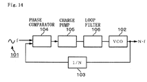
- a phase comparator 104 compares a standard signal 101 and a signal that a frequency divider circuit 103 obtains by frequency-dividing an output signal of a voltage-controlled oscillator 102, and a charge pump 105 gives a signal according to a phase difference between these signals and supplies its output to the voltage-controlled oscillator 102 via a loop filter 106, whereby the PLL circuit performs PLL control to generate a high-accuracy signal (patent document 1).
- Patent document 1 Japanese Patent Application Laid-open No. 2001-326573
- the present invention was made under such circumstances and has its object to provide a PLL apparatus realizing extremely high frequency stability.
- a PLL apparatus of the present invention includes:
- the voltage-controlled oscillation unit is, for example, an oven-controlled crystal oscillator.
- the means for supplying the voltage-controlled oscillation unit with the direct-current voltage may include: a pulse width modulation unit outputting a pulse train with a duty ratio according to the angular velocity of the vector; and a means for smoothing the pulse train output from the pulse width modulation unit.
- a preferable example of the angular velocity calculation means is one which executes an arithmetic operation of ⁇ Q(n) - Q(n - 1) ⁇ •I(n)- ⁇ I(n) - I(n - 1) ⁇ •Q(n), where I(n) and Q(n) are respectively the real part and the imaginary part corresponding to the sampling value at a given timing, and I(n - 1) and Q(n - 1) are respectively the real part and the imaginary part corresponding to the sampling value at a timing preceding the given timing.
- the external standard signal is sampled based on the frequency signal (oscillation output) from the voltage-controlled oscillation unit, the phase difference therebetween is expressed by the vector, and the oscillation output is controlled according to the angular velocity of the vector. That is, the vector is in a stopped state under the constant phase difference, but if the phase difference changes, the vector rotates, so that the loop operates so as to stop the vector.
- the present invention since the phase difference between the frequency signal from the voltage-controlled oscillation unit and the external standard signal is expressed by a digital value, by adjusting the bit numbers thereof, it is possible to make the phase difference constant with high accuracy, and providing that the standard signal has high frequency stability, it is possible to obtain a frequency signal with a desired frequency having extremely high frequency stability (on the condition that the frequency is twice the frequency of the standard signal since the standard signal is sampled). Therefore, the present invention is effective as a reference clock signal generation apparatus such as a frequency synthesizer capable of setting the frequency in a unit of 1 Hz.
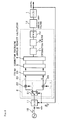
- a PLL circuit of the present invention operates based on a novel principle, and therefore, firstly, an overview of the principle of the operation of the present invention will be briefly described with reference to Fig. 1 .
- a 40 MHz frequency signal which is, for example, a rectangular wave is obtained based on an external standard signal, for example, a 10 MHz sinusoidal signal which is a standard signal obtained from, for example, a cesium frequency standard oscillator, a rubidium standard oscillator, or the like.
- This frequency signal may be a sinusoidal signal.
- the principle of the operation of the present invention is as follows.
- an A/D (analog/digital) conversion unit 11 samples the standard signal to obtain a digital signal.
- an orthogonal transformation unit 2 applies orthogonal transformation to the digital signal to extract a real part (real axis component (I)) and an imaginary part (imaginary axis component (Q)) representing a phase difference between the standard signal and the frequency signal (hereinafter, also referred to as a clock signal) from the oven-controlled crystal oscillator 1, that is, a real part (I) and an imaginary part (Q) which are complex expression of a phase vector equivalent to the phase difference.
- an angular velocity detection unit 3 detects an angular velocity of the vector
- a voltage output unit 4 generates a direct-current voltage according to the angular velocity
- the crystal oscillator 1 outputs a frequency signal according to the direct-current voltage.
- the circuit in Fig. 1 forms a PLL, and when the aforesaid phase difference is locked, the frequency signal of the crystal oscillator 1 is also stably kept at 40 MHz, providing that the standard signal is stably kept at 10 MHz.
- a portion 20 surrounded by the dotted line is provided in a computer, and units up to a unit generating a later-described PWM signal are executed by software.
- a standard signal 10 and a frequency signal from the crystal oscillator 1 are 10 MHz and 40 MHz respectively and thus are in a 1 : 4 relation, and therefore, the orthogonal transformation unit (carrier remove) 2 sequentially multiplies the digital signals from the A/D conversion unit 11 by +1, +1, thereby extracting sets of the real part (I) and the imaginary part (Q), and then it sequentially multiplies the digital signals by -1, -1, thereby extracting sets of the real part (I) and the imaginary part (Q), and by repeating this calculation, the phase difference between the standard signal 10 and the frequency signal from the crystal oscillator 1 can be monitored.
- the orthogonal transformation unit (carrier remove) 2 sequentially multiplies the digital signals from the A/D conversion unit 11 by +1, +1, thereby extracting sets of the real part (I) and the imaginary part (Q), and then it sequentially multiplies the digital signals by -1, -1, thereby extracting sets of the real part (I) and the imaginary part (Q
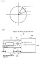
- FIG. 3 A state of this calculation is shown in Figs. 3 .
- the sampling timing of the standard signal 10 is delayed by ⁇
- the sampling is performed at timings marked by the circles shown in Fig. 3(a) . Therefore, when each of the first two sampling values is multiplied by +1, a real part and an imaginary part of a vector deviated in phase from the I axis (real axis) by - ⁇ as shown in Fig. 3(b) are obtained as a set of values.
- a switch 21 is sequentially changed based on the frequency signal from the crystal oscillator 1 and a multiplying unit 22 in a selected line multiplies the output of the A/D conversion unit 11 by +1 and -1 alternately to obtain the real parts, and a multiplying unit 23 in the selected other line multiplies the output of the A/D conversion unit 11 by +1 and -1 alternately to obtain the imaginary parts.
- a filter 24 On a subsequent stage of the orthogonal transformation unit 2, a filter 24 is provided. This filter 24 has a function of reducing attenuation distortion of a band of the external standard signal to reduce unnecessary band.
- a correction processing unit 5 applying correction processing to an I value as the real part of the vector and a Q value as the imaginary part of the vector is provided. This correction processing unit 5 divides the I value and the Q value by a scalar quantity of the vector to find the I value and the Q value per unit length of the vector. That is, as shown in Fig.
- the correction processing unit 5 squares the I value and the Q value to add the squared values and calculates a square root of the addition value to find the scalar quantity
- the reason for thus correcting the I value and the Q value is as follows.
- this is estimated based on a factor including a vector ⁇ V connecting a vector V(n) obtained in the n-th sampling and a vector V(n - 1) obtained in the (n - 1)-th sampling, as shown in Fig. 5 . Therefore, if the vector ⁇ V is, what is called, elongated to ⁇ V' due to, for example, fluctuation of a waveform of the standard signal, the correspondence relation between ⁇ V and a rotation amount ⁇ is broken, which may possibly deteriorate reliability of a detection value of the angular velocity of the vector. Therefore, by the aforesaid correction processing, the I values and the Q values at respective timings can all be uniformly changed to values corresponding to the unit length of the vector, which can eliminate the influence of the elongation of the vector.
- an angular velocity calculation unit 6 for calculating the angular velocity of the vector is provided on a subsequent stage of the correction processing unit 5.
- the angular velocity calculation unit 6 has a function of finding the angular velocity of the vector, which means that it has a function of detecting a change amount of the phase difference.
- the angular velocity calculation unit 6 will be described with reference to Fig. 6 and Fig. 7 . As shown in Fig.
- ⁇ is a difference between a phase ⁇ of V(n) and a phase ⁇ (n - 1) of V(n - 1), imag is the imaginary part, and conj ⁇ V(n) ⁇ is a conjugate vector of V(n).
- ⁇ K • imag ⁇ V • conj V n
- ⁇ V and conj ⁇ V(n) ⁇ are complex-expressed by the expression (2) and the expression (3), where I(n) and Q(n) are the I value and the Q value, respectively, corresponding to the n-th sampling.
- the angular velocity calculation unit 6 finds an approximate value of ⁇ by calculating the expression (7), and is structured as shown in Fig. 7 . If the I value input to the angular velocity calculation unit 6 is I(n) which is a value corresponding to the n-th sampling, a register 61 is holding I(n - 1) corresponding to the (n - 1)-th sampling which is an immediately preceding timing, and a comparator circuit unit 62 compares these values to extract the difference ⁇ I between I(n) and I(n - 1) and inputs I(n) and ⁇ I to a calculation unit 65.
- the Q value is similarly processed by a register 63 and a comparator circuit unit 64, and Q(n) and ⁇ Q are input to the calculation unit 65. Then, the calculation unit 65 finds ⁇ by calculating the expression (4). To be in more detail, the calculation result of the calculation unit 65 is estimated ⁇ .
- an integration circuit unit 71 integrating the angular velocities calculated by the angular velocity calculation unit, a lag-lead filter 72 smoothing an integration value from the integration circuit unit 71, and a PWM control unit 73 outputting a pulse train PWM-controlled based on the output value from the lag-lead filter 72 are provided in this order.
- the PWM control unit 73 has a function of outputting the pulse train whose duty ratio is controlled based on the output value from the lag-lead filter 72 and outputs the pulse train with the duty ratio according to the output value every 100 ms, for instance.
- an analog loop filter 12 On a subsequent stage of the PWM control unit 73, an analog loop filter 12 is provided, and this analog loop filter 12 has a function of integrating the pulse train from the PWM control unit 73 to smooth it into a direct-current voltage and supplying the direct-current voltage to a control terminal of the crystal oscillator 1.
- the PWM control unit 73 and the analog loop filter 12 correspond to the voltage output unit 4 in Fig. 1 .
- the PWM control unit 73 and the analog loop filter 12 will be more concretely described.
- the PWM control unit 73 when the angular velocity of the vector is zero (if there is no change in the phase difference), the PWM control unit 73 outputs a pulse train with a 50% duty ratio based on the output value from the lag-lead filter 72 only for 100 ms, for instance. If the level of this pulse train is 4 V, the output voltage of the analog loop filter 12, that is, an input voltage of the crystal oscillator 1 is +2 V corresponding to 50%. Then, when the vector rotates, a pulse train with a duty ratio according to the angle velocity is output from the PWM control unit 73.
- a relation between the input value of the PWM control unit 73 and the output value of the analog loop filter 12 can be that shown in Fig. 9 , for instance.
- the horizontal axis represents a value corresponding to the rotation angle of the vector.
- the operation of the above-described embodiment will be described.
- the 40 MHz frequency signal which is, for example, a rectangular wave
- the crystal oscillator 1 the external 10 MHz standard signal is sampled, and the sampling values are given to the orthogonal transformation unit 2.
- the switch 21 is switched alternately to the I value side and the Q value side based on the 40 MHz clock as previously described, and therefore, a set of the I value and the Q value is extracted in response to a 20 MHz clock.
- the I value and the Q value correspond to the real axis component and the imaginary axis component of the vector V when the vector having the phase difference ⁇ between the 40 MHz frequency signal from the crystal oscillator 1 and the 10 MHz standard signal is expressed in a complex plane.
- these I value and Q value are subjected to high-band component removal processing in the filter 24, and subsequently, the correction processing unit 5 performs the correction processing (see Fig. 4 and Fig. 5 ) of the vector V determined by the I value and the Q value as previously described.
- the angular velocity calculation unit 6 finds the angular velocity ⁇ of the vector V as shown in Fig. 7 .
- the angular velocity ⁇ is estimated based on the length of the vector ⁇ V connecting the vector V(n - 1) at a given timing and the vector V(n) at the next timing (this timing is a timing of the 20 MHz clock).
- the values of the angular velocity thus obtained are integrated and smoothed, so that the pulse train with a duty ratio corresponding to the resulting value is generated. Next, this pulse train is smoothed and as a result the direct-current voltage is generated, so that the output frequency of the crystal oscillator 1 is controlled by the direct-current voltage.
- the external standard signal is stably kept at 10 MHz
- the four sampling points in one cycle of the standard signal are at positions deviated in phase by ⁇ from 0 degree, 90 degrees, 180 degrees, and 270 degrees respectively as shown in Fig. 3(a) . Therefore, in this case, the phase difference between the standard signal and the frequency signal of the crystal oscillator 1 is constantly ⁇ , and the vector V is in a stopped state, as shown in Fig. 3(b) .
- ⁇ is zero for simplifying the illustration of the drawing.
- the PWM control unit 73 outputs a pulse train with a 50% duty ratio, the crystal oscillator 1 is supplied with a 2 V voltage, and its output frequency is 40 MHz.
- the sampling timings which have been 0 degree, 90 degrees, 180 degrees, and 270 degrees as shown in Fig. 11(a) change to 0 degree, ⁇ , 90 degrees + 2 ⁇ , 180 degrees + 3 ⁇ , and 270 degrees + 4 ⁇ and the vector V starts rotating right at the angular velocity ⁇ as shown in Fig. 11(b) .
- the angular velocity is ⁇ /25 ns, but is written as ⁇ for convenience sake.
- the duty ratio increases, so that the input voltage of the crystal oscillator 1 increases, its output frequency increases by the angular velocity ⁇ , that is, by an amount corresponding to the change amount ⁇ of the phase difference, and as a result, the output frequency of the crystal oscillator 1 is locked to 40 MHz.
- the A/D conversion unit 11 samples the external standard signal based on the frequency signal from the voltage-controlled oscillator 1, the vector is obtained as a result of the orthogonal transformation of the sampling value, and the vector is monitored. Therefore, since the phase difference between the frequency signal from the crystal oscillator 1 and the standard signal is handled as a digital value, it is possible to fix the phase difference highly accurately by adjusting the bit numbers of the digital value, and when the standard signal has high frequency stability, it is possible to obtain the frequency signal with a desired frequency with extremely high frequency stability. Further, the digital filter unit 72 and the analog loop filter 12 can adjust the frequency lead-in time by the time constant, and by adjusting the lead-in time to, for example, about 10 seconds by such adjustment, it is possible to prevent frequency jump.
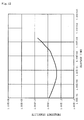
- Fig. 12 shows a frequency stability characteristic of the OCXO.
- the OCXO has good short-term stability but the stability tends to worsen with time.
- Fig. 13 by incorporating the OCXO into the above-described embodiment, good long-term stability similar to the short-term stability can be realized.
- the relation between the frequency of the standard signal and the output frequency of the voltage-controlled oscillation unit is not limited to 1 : 4.
- This ratio may be any, but the output frequency of the voltage-controlled oscillation unit needs to be twice as high as the frequency of the standard signal or more. Even when the ratio of the both frequencies is not 1 : 4, it is possible to find the I value and the Q value by selecting the frequencies based on the sampling theorem.
- an orthogonal transformation unit generally uses a sinusoidal signal with a ⁇ 0t/2 ⁇ frequency ( ⁇ 0 angular velocity) when performing quadrature detection of a sinusoidal signal which is specified by the digital signal from the A/D conversion unit 11, and can extract a vector which rotates at a frequency equal to a difference between the frequency of the frequency signal specified by the digital signal of the A/D conversion unit 11 and the frequency of the sinusoidal signal used in the detection.
- the real part and the imaginary part which are complex expression of this vector can be extracted.
- the carrier remove can have the output line of the A/D conversion unit 11 branch off, and can include a multiplying unit multiplying the sinusoidal signal by cos( ⁇ 0t), a multiplying unit multiplying the sinusoidal signal by -sin( ⁇ 0t), and low-pass filters provided on subsequent stages of these multiplying units.
Landscapes
- Stabilization Of Oscillater, Synchronisation, Frequency Synthesizers (AREA)
Applications Claiming Priority (2)
| Application Number | Priority Date | Filing Date | Title |
|---|---|---|---|
| JP2006100652A JP4356947B2 (ja) | 2006-03-31 | 2006-03-31 | Pll装置 |
| PCT/JP2007/057686 WO2007114498A1 (ja) | 2006-03-31 | 2007-03-30 | Pll装置 |
Publications (4)
| Publication Number | Publication Date |
|---|---|
| EP2003779A2 true EP2003779A2 (de) | 2008-12-17 |
| EP2003779A9 EP2003779A9 (de) | 2009-05-20 |
| EP2003779A4 EP2003779A4 (de) | 2010-04-14 |
| EP2003779B1 EP2003779B1 (de) | 2010-12-22 |
Family
ID=38563757
Family Applications (1)
| Application Number | Title | Priority Date | Filing Date |
|---|---|---|---|
| EP07741122A Ceased EP2003779B1 (de) | 2006-03-31 | 2007-03-30 | Phasenregelkreiselement |
Country Status (6)
| Country | Link |
|---|---|
| US (1) | US7812651B2 (de) |
| EP (1) | EP2003779B1 (de) |
| JP (1) | JP4356947B2 (de) |
| CN (1) | CN101416392B (de) |
| DE (1) | DE602007011413D1 (de) |
| WO (1) | WO2007114498A1 (de) |
Families Citing this family (3)
| Publication number | Priority date | Publication date | Assignee | Title |
|---|---|---|---|---|
| JP4356946B2 (ja) * | 2006-03-31 | 2009-11-04 | 日本電波工業株式会社 | Pll装置 |
| US8330509B2 (en) * | 2010-04-12 | 2012-12-11 | Intel Mobile Communications GmbH | Suppression of low-frequency noise from phase detector in phase control loop |
| CN101841329A (zh) * | 2010-06-12 | 2010-09-22 | 中兴通讯股份有限公司 | 锁相环、压控装置及方法 |
Family Cites Families (11)
| Publication number | Priority date | Publication date | Assignee | Title |
|---|---|---|---|---|
| GB9122711D0 (en) * | 1991-10-25 | 1991-12-11 | Alpha Image Ltd | Digitally phase locking analogue signals |
| US6304620B1 (en) * | 1998-03-20 | 2001-10-16 | Philips Electronics North America Corproation | Sign-cross product automatic frequency control loop |
| US6198353B1 (en) * | 1999-08-05 | 2001-03-06 | Lucent Technologies, Inc. | Phase locked loop having direct digital synthesizer dividers and improved phase detector |
| JP2001326573A (ja) | 2000-05-18 | 2001-11-22 | Nec Eng Ltd | クロック切替装置及びクロック切替方法 |
| US7099642B2 (en) * | 2001-11-09 | 2006-08-29 | Qualcomm, Incorporated | Method and apparatus for matching receiver carrier frequency |
| JP2003289248A (ja) | 2002-03-27 | 2003-10-10 | Sharp Corp | Pll回路 |
| DE60208964T2 (de) * | 2002-11-21 | 2006-10-26 | Sony Ericsson Mobile Communications Ab | Oszillatorfrequenzsteuerung |
| JP4168329B2 (ja) * | 2003-01-29 | 2008-10-22 | ソニー株式会社 | 位相波形ゲイン制御装置 |
| JP2005109551A (ja) * | 2003-09-26 | 2005-04-21 | Matsushita Electric Ind Co Ltd | Pll回路 |
| US7242224B1 (en) * | 2004-02-20 | 2007-07-10 | Marvell International Ltd. | Continuous, wide-range frequency synthesis and phase tracking methods and apparatus |
| JP4356946B2 (ja) * | 2006-03-31 | 2009-11-04 | 日本電波工業株式会社 | Pll装置 |
-
2006
- 2006-03-31 JP JP2006100652A patent/JP4356947B2/ja not_active Expired - Lifetime
-
2007
- 2007-03-30 EP EP07741122A patent/EP2003779B1/de not_active Ceased
- 2007-03-30 DE DE602007011413T patent/DE602007011413D1/de active Active
- 2007-03-30 CN CN2007800115963A patent/CN101416392B/zh active Active
- 2007-03-30 US US12/225,573 patent/US7812651B2/en active Active
- 2007-03-30 WO PCT/JP2007/057686 patent/WO2007114498A1/ja not_active Ceased
Also Published As
| Publication number | Publication date |
|---|---|
| US20090167382A1 (en) | 2009-07-02 |
| EP2003779A4 (de) | 2010-04-14 |
| DE602007011413D1 (de) | 2011-02-03 |
| WO2007114498A1 (ja) | 2007-10-11 |
| JP2007274615A (ja) | 2007-10-18 |
| EP2003779A9 (de) | 2009-05-20 |
| EP2003779B1 (de) | 2010-12-22 |
| CN101416392B (zh) | 2011-08-24 |
| JP4356947B2 (ja) | 2009-11-04 |
| CN101416392A (zh) | 2009-04-22 |
| US7812651B2 (en) | 2010-10-12 |
Similar Documents
| Publication | Publication Date | Title |
|---|---|---|
| EP2003780B1 (de) | Phasenregelkreiselement | |
| US7061276B2 (en) | Digital phase detector | |
| EP3203260B1 (de) | Signalerzeugungsschaltung | |
| JP4924630B2 (ja) | クロック生成回路 | |
| CN101873135A (zh) | 频率合成器 | |
| EP2003779B1 (de) | Phasenregelkreiselement | |
| US20140072084A1 (en) | Digital system and method of estimating quasi-harmonic signal non-energy parameters using a digital Phase Locked Loop | |
| EP2663017B1 (de) | Verfahren zur Synchronisierungsabtastung an sinusförmigen Eingängen | |
| US7764207B2 (en) | Digital processor | |
| US7215273B2 (en) | Method and device for reconstructing and controlling the phase position of a sampling clock relative to an analog signal to be sampled | |
| JP4935166B2 (ja) | 電力変換装置の位相同期制御装置 | |
| US8466724B2 (en) | Frequency synthesizer | |
| US9729157B2 (en) | Variable clock phase generation method and system | |
| JP5560781B2 (ja) | 周波数シンセサイザ及び周波数シンセサイザの調整方法 | |
| KR101250571B1 (ko) | 주파수 신시사이저 | |
| JP2008147788A (ja) | 位相同期回路、同期検波回路および放送受信装置 |
Legal Events
| Date | Code | Title | Description |
|---|---|---|---|
| PUAI | Public reference made under article 153(3) epc to a published international application that has entered the european phase |
Free format text: ORIGINAL CODE: 0009012 |
|
| 17P | Request for examination filed |
Effective date: 20080924 |
|
| AK | Designated contracting states |
Kind code of ref document: A2 Designated state(s): DE FR GB IT |
|
| PUAB | Information related to the publication of an a document modified or deleted |
Free format text: ORIGINAL CODE: 0009199EPPU |
|
| RBV | Designated contracting states (corrected) |
Designated state(s): DE FR GB IT |
|
| A4 | Supplementary search report drawn up and despatched |
Effective date: 20100312 |
|
| RIC1 | Information provided on ipc code assigned before grant |
Ipc: H03L 7/091 20060101AFI20100308BHEP Ipc: H03L 7/093 20060101ALI20100308BHEP |
|
| GRAP | Despatch of communication of intention to grant a patent |
Free format text: ORIGINAL CODE: EPIDOSNIGR1 |
|
| RIC1 | Information provided on ipc code assigned before grant |
Ipc: H03L 7/091 20060101AFI20100618BHEP Ipc: H03L 7/093 20060101ALI20100618BHEP |
|
| GRAS | Grant fee paid |
Free format text: ORIGINAL CODE: EPIDOSNIGR3 |
|
| GRAA | (expected) grant |
Free format text: ORIGINAL CODE: 0009210 |
|
| AK | Designated contracting states |
Kind code of ref document: B1 Designated state(s): DE FR GB IT |
|
| REG | Reference to a national code |
Ref country code: GB Ref legal event code: FG4D |
|
| REF | Corresponds to: |
Ref document number: 602007011413 Country of ref document: DE Date of ref document: 20110203 Kind code of ref document: P |
|
| REG | Reference to a national code |
Ref country code: DE Ref legal event code: R096 Ref document number: 602007011413 Country of ref document: DE Effective date: 20110203 |
|
| PLBE | No opposition filed within time limit |
Free format text: ORIGINAL CODE: 0009261 |
|
| STAA | Information on the status of an ep patent application or granted ep patent |
Free format text: STATUS: NO OPPOSITION FILED WITHIN TIME LIMIT |
|
| 26N | No opposition filed |
Effective date: 20110923 |
|
| REG | Reference to a national code |
Ref country code: DE Ref legal event code: R097 Ref document number: 602007011413 Country of ref document: DE Effective date: 20110923 |
|
| REG | Reference to a national code |
Ref country code: FR Ref legal event code: PLFP Year of fee payment: 10 |
|
| REG | Reference to a national code |
Ref country code: FR Ref legal event code: PLFP Year of fee payment: 11 |
|
| REG | Reference to a national code |
Ref country code: FR Ref legal event code: PLFP Year of fee payment: 12 |
|
| PGFP | Annual fee paid to national office [announced via postgrant information from national office to epo] |
Ref country code: GB Payment date: 20190327 Year of fee payment: 13 |
|
| PGFP | Annual fee paid to national office [announced via postgrant information from national office to epo] |
Ref country code: DE Payment date: 20200317 Year of fee payment: 14 Ref country code: IT Payment date: 20200221 Year of fee payment: 14 |
|
| PGFP | Annual fee paid to national office [announced via postgrant information from national office to epo] |
Ref country code: FR Payment date: 20200214 Year of fee payment: 14 |
|
| GBPC | Gb: european patent ceased through non-payment of renewal fee |
Effective date: 20200330 |
|
| PG25 | Lapsed in a contracting state [announced via postgrant information from national office to epo] |
Ref country code: GB Free format text: LAPSE BECAUSE OF NON-PAYMENT OF DUE FEES Effective date: 20200330 |
|
| REG | Reference to a national code |
Ref country code: DE Ref legal event code: R119 Ref document number: 602007011413 Country of ref document: DE |
|
| PG25 | Lapsed in a contracting state [announced via postgrant information from national office to epo] |
Ref country code: DE Free format text: LAPSE BECAUSE OF NON-PAYMENT OF DUE FEES Effective date: 20211001 Ref country code: FR Free format text: LAPSE BECAUSE OF NON-PAYMENT OF DUE FEES Effective date: 20210331 |
|
| PG25 | Lapsed in a contracting state [announced via postgrant information from national office to epo] |
Ref country code: IT Free format text: LAPSE BECAUSE OF NON-PAYMENT OF DUE FEES Effective date: 20210330 |