EP2003873A2 - Capteur d'images et procédé de lecture - Google Patents
Capteur d'images et procédé de lecture Download PDFInfo
- Publication number
- EP2003873A2 EP2003873A2 EP08010620A EP08010620A EP2003873A2 EP 2003873 A2 EP2003873 A2 EP 2003873A2 EP 08010620 A EP08010620 A EP 08010620A EP 08010620 A EP08010620 A EP 08010620A EP 2003873 A2 EP2003873 A2 EP 2003873A2
- Authority
- EP
- European Patent Office
- Prior art keywords
- image sensor
- column
- output
- columns
- line
- Prior art date
- Legal status (The legal status is an assumption and is not a legal conclusion. Google has not performed a legal analysis and makes no representation as to the accuracy of the status listed.)
- Granted
Links
Images


Classifications
-
- H—ELECTRICITY
- H04—ELECTRIC COMMUNICATION TECHNIQUE
- H04N—PICTORIAL COMMUNICATION, e.g. TELEVISION
- H04N25/00—Circuitry of solid-state image sensors [SSIS]; Control thereof
-
- H—ELECTRICITY
- H04—ELECTRIC COMMUNICATION TECHNIQUE
- H04N—PICTORIAL COMMUNICATION, e.g. TELEVISION
- H04N25/00—Circuitry of solid-state image sensors [SSIS]; Control thereof
- H04N25/60—Noise processing, e.g. detecting, correcting, reducing or removing noise
- H04N25/62—Detection or reduction of noise due to excess charges produced by the exposure, e.g. smear, blooming, ghost image, crosstalk or leakage between pixels
- H04N25/626—Reduction of noise due to residual charges remaining after image readout, e.g. to remove ghost images or afterimages
-
- H—ELECTRICITY
- H04—ELECTRIC COMMUNICATION TECHNIQUE
- H04N—PICTORIAL COMMUNICATION, e.g. TELEVISION
- H04N25/00—Circuitry of solid-state image sensors [SSIS]; Control thereof
- H04N25/60—Noise processing, e.g. detecting, correcting, reducing or removing noise
- H04N25/67—Noise processing, e.g. detecting, correcting, reducing or removing noise applied to fixed-pattern noise, e.g. non-uniformity of response
- H04N25/671—Noise processing, e.g. detecting, correcting, reducing or removing noise applied to fixed-pattern noise, e.g. non-uniformity of response for non-uniformity detection or correction
- H04N25/677—Noise processing, e.g. detecting, correcting, reducing or removing noise applied to fixed-pattern noise, e.g. non-uniformity of response for non-uniformity detection or correction for reducing the column or line fixed pattern noise
-
- H—ELECTRICITY
- H04—ELECTRIC COMMUNICATION TECHNIQUE
- H04N—PICTORIAL COMMUNICATION, e.g. TELEVISION
- H04N25/00—Circuitry of solid-state image sensors [SSIS]; Control thereof
- H04N25/70—SSIS architectures; Circuits associated therewith
- H04N25/76—Addressed sensors, e.g. MOS or CMOS sensors
-
- H—ELECTRICITY
- H04—ELECTRIC COMMUNICATION TECHNIQUE
- H04N—PICTORIAL COMMUNICATION, e.g. TELEVISION
- H04N25/00—Circuitry of solid-state image sensors [SSIS]; Control thereof
- H04N25/70—SSIS architectures; Circuits associated therewith
- H04N25/76—Addressed sensors, e.g. MOS or CMOS sensors
- H04N25/766—Addressed sensors, e.g. MOS or CMOS sensors comprising control or output lines used for a plurality of functions, e.g. for pixel output, driving, reset or power
-
- H—ELECTRICITY
- H04—ELECTRIC COMMUNICATION TECHNIQUE
- H04N—PICTORIAL COMMUNICATION, e.g. TELEVISION
- H04N25/00—Circuitry of solid-state image sensors [SSIS]; Control thereof
- H04N25/70—SSIS architectures; Circuits associated therewith
- H04N25/76—Addressed sensors, e.g. MOS or CMOS sensors
- H04N25/767—Horizontal readout lines, multiplexers or registers
-
- H—ELECTRICITY
- H04—ELECTRIC COMMUNICATION TECHNIQUE
- H04N—PICTORIAL COMMUNICATION, e.g. TELEVISION
- H04N25/00—Circuitry of solid-state image sensors [SSIS]; Control thereof
- H04N25/70—SSIS architectures; Circuits associated therewith
- H04N25/76—Addressed sensors, e.g. MOS or CMOS sensors
- H04N25/78—Readout circuits for addressed sensors, e.g. output amplifiers or A/D converters
Definitions
- the present invention relates to an image sensor, in particular CMOS image sensor, for electronic cameras, comprising a plurality of light-sensitive pixels arranged in rows and columns, further comprising a number of output amplifiers, further comprising a switching device for selectively connecting the pixels of one of the lines to the output amplifiers to switch, and with a control device for controlling the switching device.
- CMOS image sensor for electronic cameras, comprising a plurality of light-sensitive pixels arranged in rows and columns, further comprising a number of output amplifiers, further comprising a switching device for selectively connecting the pixels of one of the lines to the output amplifiers to switch, and with a control device for controlling the switching device.
- Known electronic cameras include an image sensor comprising a plurality of light-sensitive elements or pixels arranged in rows and columns, which convert light falling through a lens of the camera into electrical signals. For reading an image, each of the pixels is addressed, and a signal proportional to a charge of the pixel collected by an exposure is sent to an output of the image sensor.
- image sensors In cameras, which simultaneously have a high number of photosensitive elements and a high frame rate, image sensors are used which have a plurality of outputs a, which can be read in parallel in a respective read cycle - and thus faster.
- the columns may be divided into column groups each having a plurality of columns, the number of columns in each of the column groups corresponding to the number of outputs.
- the columns are assigned to the outputs of the image sensor in the manner of adjacent unit matrices, so that the columns with the numbers n, n + a, n + 2a, etc. are each assigned to the output with the number n, the columns and the outputs each numbered consecutively.
- the first column of the image sensor corresponding to the first column of the first column group is assigned to the first output.
- the 2nd column of the image sensor, which corresponds to the 2nd column of the 1st column group, is assigned to the 2nd output, etc., up to the 32nd column of the image sensor, which corresponds to the 32nd column of the 1st column group corresponding to the 32nd column Output is assigned.
- the 33rd column of the image sensor which corresponds to the 1st column of the 2nd column group, is again assigned to the 1st output
- the 34th column of the image sensor which corresponds to the 2nd column of the 2nd column group, again to the 1st column 2nd output assigned etc ..
- Each of the outputs of the image sensor has its own output amplifier, whereby the output amplifiers amplify the signals of the pixels for subsequent digitization.
- the signals are applied to the output amplifiers as analog electrical voltages corresponding to the collected charges.
- the readout of such an image sensor is usually done line by line, ie line by line.
- the signals of the assigned pixels are switched to the outputs of the image sensor by means of corresponding control signals, column by column, ie, column by column, or possibly column group-wise, ie, column group by column group.
- the reading starts at a first column group located at an edge of the image sensor and continues in ascending order with the immediately adjacent column group, that is, according to the arrangement order of the columns or column groups. It follows that at the 1st output or 1st output amplifier, the signals of the pixels of the 1st, 33rd, 65th, etc. column of the image sensor are successively output, at the 2nd output or 2nd output amplifier, the signals of Pixels of the 2nd, 34th, 66th, etc. columns of the image sensor are output, etc.
- the image sensor has only a single output and thus only one output amplifier, the signals of all pixels are amplified by the same output amplifier, the signals immediately adjacent pixels are amplified immediately after one another, so that the proportion of the signal of the respective previous pixel in the signal of the respective Predecessor pixels immediately adjacent arranged pixels takes effect. Although this produces a kind of blurring in the image with large differences between two directly successively amplified signals. However, this is not perceptible with the eye.
- the proportion of the signal of the respective predecessor pixel-that is to say the proportion of the directly previously amplified signal-becomes noticeable in the amplification of the signal of the pixel which is the number of outputs from the predecessor pixel is arranged remotely.
- the signals of the pixels located between the predecessor pixel and the pixel removed by the number of outputs from the predecessor pixel are amplified by the output amplifiers of the remaining outputs.
- a visual echo of the candle flame is generated laterally offset from the original candle flame.
- Such a picture disturbance is called ghosting.
- the ghost image is particularly visible because the echo occurs in a dark area.
- the echo is 32 pixels from the original.
- the invention has for its object to provide an image sensor of the type mentioned, which makes it possible to suppress the formation of ghost images.
- an image sensor having the features of claim 1, and in particular by the order in which the pixels are switched to the output amplifiers being varied in relation to the order in which the pixels are arranged along one row of the image sensor.
- the signals of the pixels of a line can also be read out by column groups, i. the signals of the pixels of a column group of the respective row can be read together in a respective read cycle, or the signals of the pixels of a row are read out column by column.
- the signals of the pixels according to such a spatial or temporal order from column to column or possibly within a respective column group (ie within a read cycle) or column group to column group (ie from read cycle to read cycle) on the switched individual output amplifier, which is different in the order in which the pixels are arranged along the respective line of the image sensor.
- This change in the switching order or the pixel spacing is at least for a plurality of output amplifiers, preferably for all output amplifiers.
- the columns are divided into a plurality of column groups, and the number of output amplifiers corresponds to the number of columns of a column group, the columns of each column group are assigned to the output amplifiers according to a mapping order, and a plurality of mutually different assignment orders are provided for the plurality of column groups ,
- the orders in which the columns are (and thus the pixels) of a respective column group are assigned to the output amplifiers of the image sensor, different for the plurality of column groups.
- the assignment of the individual columns of a respective column group to the output amplifiers of the image sensor is thus not or not exclusively according to the above-described type of a unit matrix.
- a respective assignment order is predetermined, for example, by the distribution of allocation points at which a column of the image sensor is linked or connectable to a respective horizontal output line of a signal bus, which in turn can be switched to a specific one of the plurality of output amplifiers of the image sensor.
- These allocation points are either fixed (by permanent electrical connection between the relevant column line and the relevant output line). Or, variably assignable allocation points are provided, wherein a respective switch is arranged at the relevant allocation points.
- the column groups have mutually different assignment orders.
- the assignment order of the columns of a column group to the output amplifiers is thus different from the assignment order of the columns of another column group to the output amplifiers.
- the assignment orders of all column groups may be different.
- the odd-numbered column groups of the image sensor may have a first allocation order and the even-numbered column groups may have a second allocation order, wherein the first and second allocation order are different from each other.
- the arrangement order of the column groups corresponds to the read order of the column groups, sufficient scramble of ghost images can be achieved.
- a plurality of signal buses are provided, each comprising a number of output lines, which corresponds to the number of output amplifiers, wherein the signal buses are selectively switched to the output amplifier, in particular by means of a switching device designed as a multiplexer device.
- the output lines of the signal buses are designed to connect the output amplifiers to the columns of the column groups.
- the control device may be designed to control the switching device in such a way that two column groups connected in succession to the output amplifiers are switched to the output amplifiers via different ones of the signal buses.
- some or all of the column groups are associated with multiple or all of the signal buses, with the allocation orders within each such column group being different for the respective signal buses.
- this makes it possible for the allocation order within a column group to be varied from line to line.
- the columns of the relevant column group can be switched from line to line to different signal buses. As a result, a further scrambling can be achieved.
- control device is designed to control the switching device in such a way, that the signal busses are switched from row to row in different order to the output amplifiers.
- the image sensor According to a development of the image sensor using a read-out sequence is completely readable, the image sensor, however, has more signal buses, as are actually required for reading according to a regular read-out sequence. Consequently, a redundant signal bus is provided with regard to a complete readout. For example, if the image sensor has 5 signal busses but only 4 signal busses are required for readout, if one of the signal busses is defective, a bus allocation order may be used in which the defective signal bus is not used.
- the image sensor is controlled such that the time reading order according to which the column groups are successively connected to the output amplifiers is different from the arrangement order according to which the column groups are in the direction a row are arranged side by side, wherein the columns are divided into a plurality of column groups and the number of output amplifiers corresponds to the number of columns of a column group.
- the different column groups are not switched in the same order to the output amplifiers in which the column groups are arranged side by side.
- a ghost image whose original extends across several column groups is divided along the boundaries of the column groups, whereby the individual portions of the ghost image may appear scrambled at different positions within the image, such that the ghost image is no longer perceptible to the eye is. It is particularly effective if the varying of the chronological order of the read-out of the column groups is combined with the explained variation of the spatial assignment order of the columns to the output amplifiers.
- the columns may also be arranged relative to each other according to an arrangement order and the control means may be configured to control the switching means such that the columns for each row are sequentially switched to the output amplifiers according to a respective readout order The reading order of the columns is different from the arrangement order of the columns.
- this scrambling can be further improved by also varying the reading order from line to line.
- the image sensor has at least one signal bus, which in each case comprises a number of output lines which corresponds to the number of output amplifiers, wherein the columns can be connected at predetermined assignment points to a plurality or all of the output lines of the at least one signal bus. This allows any assignment of the columns to the output amplifiers. As a result, a defective output can be bypassed.
- the invention also relates to a corresponding method for reading out an image sensor, in particular a CMOS image sensor, for electronic cameras.
- a non-limiting embodiment of the invention which illustrates a combination of several measures for scrambling a ghost, is shown in the drawing and will be described below.
- the in Fig. 1 The image sensor shown has a plurality of photosensitive pixels P arranged in lines (shown horizontally here) and columns (shown vertically here). For the sake of clarity, only one of the pixels P is provided with a reference numeral.
- Each row has a row selection line..., Z m-1 , Z m for the pixels P associated with the respective row, and each column comprises a column line S 1-1 ,..., S 1-4 , S 2-1 , ..., S 2-4 , ... for the pixel P associated with each column.
- the column lines S 1-1 , ..., S 1-4 , S 2-1 , ..., S 2-4 , ... are subdivided into column groups S 1 , S 2 ,..., each having four column lines S 1-1 ,..., S 1-4 , S 2-1 ,..., S 2-4 , ... include.
- the image sensor further comprises a line selection circuit 11, through which in each case one of the lines..., Z m-1 , Z m for reading out the signals of the pixels P this line ..., Z m-1 , Z m can be selected.
- a column selection circuit 13 is provided, by means of which one of the plurality of column groups S 1 , S 2 ,... Can be selected for reading the signals of the pixels P of this column group S 1 , S 2 ,.
- a separate column selection switch 19 is provided (of which only one with a reference numeral the column selection switches 19 of each column group S 1 , S 2 ,...
- the row selection circuit 11, the column selection circuit 13, the column selection switches 19, the column selection control lines 21, and optionally a bus selection circuit, bus selection switch, and a bus selection control line, which will be described later, are part of a switching device of the image sensor which is controlled by a control means such as a microcontroller. Controller 17, is controlled.
- the image sensor has a signal bus, which in the example shown here comprises four output lines A 1 , A 2 , A 3 , A 4 , to which the signals of the pixels of a line ..., Z m-1 , Z m a Column group S 1 , S 2 , ... can be switched, each of the output lines A 1 , A 2 , A 3 , A 4 is connected to its own output amplifier V 1 , V 2 , V 3 , V 4 .
- each column line S 1-1 , ..., S 1-4 , S 2-1 , ..., S 2-4 , ... of each column group S 1 , S 2 , ... a respective output line A 1 , A 2 , A 3 , A 4 and thus a single output amplifier V 1 , V 2 , V 3 , V 4 according to an assignment order assigned uniquely, wherein the column groups S 1 , S 2 , ... from each other have different assignment sequences.
- the assignments are fixed electrical connections between the column lines S 1-1 , ..., S 1-4 , S 2-1 , ..., S 2-4 , ... and the output lines A 1 , A 2 , A 3 , A 4 .
- the first column line S 1-1 of the first column group S 1 is the first output line A 1
- the second column line S 1-2 of the first column group S 1 is the third output line A 3
- Column line S 1-3 of the first column group S 1 is the second output line A 2
- the fourth column line S 1-4 of the first column group S 1 is assigned to the fourth output line A 4 , as determined using assignment points Z is recognizable.
- the reading is done line by line by applying corresponding address signals to the line selection circuit 11, wherein the line selection lines ..., Z m-1 , Z m are successively addressed starting in a first, located at one edge of the image sensor line selection line in ascending order.
- the read out is done column by column for each row, that is, the pixels P associated with each selected row are read out by corresponding control of the column selection switches 19 by the column selection circuit 13 column group by column group. Since the assignment orders of the column groups S 1 , S 2 ,... To the signal bus are different from each other, scramble of a ghost can be achieved.
- the controller 17 of the image sensor may be configured to control the column selection switches 19 by the column selecting circuit 13 so as to vary the readout order of the column groups S 1 , S 2 ,... From line to line.
- the image sensor is set up such that the read order of the column groups for at least some of the lines..., Z m-1 , Z m does not match the arrangement order of the column groups S 1 , S 2 ,.
- the column groups S 1 , S 2 , ... are therefore not read out in ascending order, that is not first the first column group S 1 , then the second column group S 2 , then the third column group S 3 , etc .. Rather the column groups S 1 , S 2 , ... quasi-random read, ie, for example, first the 37th column group S 37 , then the seventh column group S 7 , then the 22nd column group, etc ..
- a variant of the embodiment according to Fig. 1 is for the different column groups S 1 , S 2 , ... different from the illustration according to Fig. 1 always the same allocation order provided, for example, according to the known type of a unitary matrix. Scrambling of a ghost image is achieved in this case solely by varying the read order of the column groups S 1 , S 2 , ... for at least some of the lines as described in the preceding paragraph.
- two signal buses B 1 , B 2 are provided, each having four output lines A 1 , A 2 , A 3 , A 4 , wherein the odd-numbered column groups S 1 , S 3 , ... the first Signal bus B 1 and the even-numbered column groups S 2 , S 4 , ... are assigned to the second signal bus B 2 .
- any other assignment of the column groups S 1 , S 2 , S 3 , ... to the signal buses B 1 , B 2 is possible.
- the assignment sequences of the individual column groups S 1 , S 2 , S 3 , Fig. 1 shown assignment sequences, so that the in Fig. 2 shown column groups S 1 , S 2 , ... have mutually different assignment sequences.
- a controllable by the micro-controller 17 bus selection circuit 15 is provided, which makes it possible to connect via two bus selection control lines 27 optionally one of the two signal buses B 1 , B 2 to the output amplifier V 1 , V 2 , V 3 V 4 , wherein the 1st output line A 1 of the respective signal bus B 1 , B 2 to the 1st output amplifier V 1 , the 2nd output line A 2 of the respective signal bus B 1 , B 2 to the second output amplifier, the third output line A 3 of the respective Signal bus B 1 , B 2 on the 3rd output amplifier, and the 4th output line A 4 of the respective signal bus B 1 , B 2 can be switched to the 4th output amplifier.
- a separate bus selector switch 25 is provided for each of the output lines A 1 , A 2 , A 3 , A 4 (of which only two are provided with a reference numeral), wherein the bus selector switch 25 of each signal bus B 1 , B 2 via a respective common Bus selection control line 27 are controllable by the bus selection circuit 15, so that the bus selection switch 25 of each bus B 1 , B 2 are each jointly switchable.
- control device 17 of the image sensor according to Fig. 2 be designed to control the column selection switch 19 by the column selection circuit 13 such that the read order of the column groups S 1 , S 2 , ... is varied from line to line.
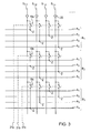
- the image sensor according to Fig. 3 has three signal buses B 1 , B 2 , B 3 and is only shown in the region of the assignment of the column group S 1 to the signal buses B 1 , B 2 , B 3 , wherein the column group S 1 is selected only by way of example.
- the column group S 1 as well as the other column groups S 2 , S 3 ,..., Not shown, is assigned to each of the three signal buses B 1 , B 2 , B 3 , the assignment sequences within each column group S 1 , S 2 , ... are different.
- first column selection switches 19a associated with the allocation points Z are B 1 for the 1st signal bus, second column selection switches 19b for the 2nd signal bus B 2 , and third column selection switches 19c for the 3rd signal bus B 3 provided (of which only one column selection switch 19 a, 19 b, 19 c is provided with a reference numeral).
- These column selection switches 19a, 19b, 19c allow the column groups S 1 , S 2 , ...
- the first column selection switches 19 a being connected via a common column selection control line 21 a
- the second column selection switches 19b via a common column selection control line 21b
- the third column selection switches 19c via a common column selection control line 21c from that in FIG Fig. 3 not shown column selection circuit are controllable, so that the column selection switches 19a, 19b or 19c are each jointly switchable.
- the first column selection switches 19a are closed, and the second and third column selection switches 19b, 19c opened.
- the second column selection switches 19b are closed and the first and third column selection switches 19a, 19c opened.
- the third column selection switch 19c are closed and the first and second column select switches 19a, 19b open.
- the structure of the image sensor according to Fig. 3 the structure of the image sensor according to Fig. 2
- analogous to the first two signal buses B 1 , B 2 in the image sensor according to Fig. 3 are also provided for the third signal bus B 3 bus selector switch, which via a common Busausuß Wenntechnisch of the in Fig. 3 Bus selector circuit, not shown, are controllable, so that either one of the three signal buses B 1 , B 2 , B 3 on the in Fig. 3 not shown output amplifier is switchable.
- the image sensor according to Fig. 3 is designed for a read-only sequence which only requires two signal busses for a complete readout, for example the two signal busses B 1 and B 2 .
- the third signal bus B 3 is a redundant signal bus which can be used as a replacement for one of the two signal buses B 1 , B 2 if one of the two signal buses B 1 , B 2 is defective.
- the signal busses are always switched in the same sequence to the output amplifiers when reading out per line, ie the sequence is cyclically repeated within the line, the sequence being varied from line to line.
- the amplified signals can be easily assigned to the respective pixels P in order to correctly assemble the amplified signals into a recording image.
- the output amplifiers V 1 , V 2 , V 3 , V 4 are switched for the readout of the column groups S 1 , S 2 ,... of the second row Z 2 in the order B 1 , B 4 , B 2 , B 3 , ..., etc.
- predetermined quasi-random sequences can be used.
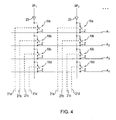
- the image sensor according to Fig. 4 is, unlike the image sensors according to the Fig. 1 to 3 , not divided into column groups and includes, besides a plurality of column lines SP 1 , SP 2 , ... a single signal bus with four output lines A 1 , A 2 , A 3 , A 4 .
- the image sensor according to Fig. 4 is shown only in the region of the assignments of the first two column lines SP 1 and SP 2 to the output lines A 1 , A 2 , A 3 , A 4 , wherein the two column lines SP 1 and SP 2 are selected only by way of example.
- the column lines SP 1 and SP 2 as well as the other column lines SP 3 , SP 4 ,..., Not shown, are assigned to each of the four output lines A 1 , A 2 , A 3 , A 4 .
- the column lines SP 1 , SP 2 , ... are respectively associated first column selection switch 19a for the 1st output line A 1 , second column selection switch 19b for the 2nd output line A 2 , third column selection switch 19c for the 3rd output line A 3 , and fourth Column selection switch 19d provided for the 4th output line A 4 .
- These column selection switches 19a, 19b, 19c, 19d allow the in Fig. 4 not shown column selection circuit, the column lines SP 1 , SP 2 , ... via respective column selection control lines 21a, 21b, 21c, 21d each optionally to a single one of the output lines A 1 , A 2 , A 3 , A 4 to switch.
- the first column selection switch 19a is closed, and the second, third, and fourth column selection switches 19b, 19c, 19d will be opened.
- the second column selection switch 19b is closed, and the first, third, and fourth column selection switches 19a, 19c, 19d are opened.
- the third column selection switch 19c is closed, and the first, the second and the fourth column selection switches 19a, 19b, 19d are open.
- the fourth column selection switch 19d is closed, and the first, the second and the third column selection switches 19a, 19b, 19c are opened.
- the structure of the image sensor according to Fig. 4 the structure of the image sensor according to Fig. 1
- the column lines SP 1 , SP 2 , ... opposite Fig. 1 are not divided into column groups.
- the image sensor according to Fig. 4 to modify such that a plurality of signal buses are provided (not shown), wherein each column line to each of the signal buses via corresponding column selection switch as above Fig. 3 is explained.
- each column line is assigned to each of the signal buses, but the respective column line is not assigned to all of the output lines of the respective signal bus.
- Fig. 1 to 4 are the signals of the pixels P of the respective row of the respective column group S 1 , S 2 , ... in the form of voltage signals to the output amplifiers V 1 , V 2 , V 3 , V 4 , then by means of an A / D converter means (not shown) each to be converted into a digital value.
- the pixels P of the image sensor are preferably active pixels in which the charge signals are already converted in the pixels P into voltage signals. In principle, however, the pixels P can also be designed as passive pixels in which the conversion of the charge signals into voltage signals takes place on the signal path from the pixels P to the output amplifiers A 1 , A 2 , A 3 , A 4 .
- the column selection switches 19 and the bus selection switches 25 may be, for example, CMOS transistors.
Landscapes
- Engineering & Computer Science (AREA)
- Multimedia (AREA)
- Signal Processing (AREA)
- Transforming Light Signals Into Electric Signals (AREA)
- Solid State Image Pick-Up Elements (AREA)
- Facsimile Heads (AREA)
Applications Claiming Priority (1)
| Application Number | Priority Date | Filing Date | Title |
|---|---|---|---|
| DE102007027463.9A DE102007027463B4 (de) | 2007-06-14 | 2007-06-14 | Bildsensor |
Publications (3)
| Publication Number | Publication Date |
|---|---|
| EP2003873A2 true EP2003873A2 (fr) | 2008-12-17 |
| EP2003873A3 EP2003873A3 (fr) | 2013-04-17 |
| EP2003873B1 EP2003873B1 (fr) | 2018-06-06 |
Family
ID=39811511
Family Applications (1)
| Application Number | Title | Priority Date | Filing Date |
|---|---|---|---|
| EP08010620.6A Active EP2003873B1 (fr) | 2007-06-14 | 2008-06-11 | Capteur d'images et procédé de lecture |
Country Status (3)
| Country | Link |
|---|---|
| US (1) | US8045031B2 (fr) |
| EP (1) | EP2003873B1 (fr) |
| DE (1) | DE102007027463B4 (fr) |
Families Citing this family (16)
| Publication number | Priority date | Publication date | Assignee | Title |
|---|---|---|---|---|
| JP4054839B1 (ja) * | 2007-03-02 | 2008-03-05 | キヤノン株式会社 | 光電変換装置およびそれを用いた撮像システム |
| US7893977B2 (en) * | 2007-10-23 | 2011-02-22 | Xerox Corporation | Multiplexing and offset correction system for an image sensor array |
| DE102009004187A1 (de) * | 2009-01-09 | 2010-07-15 | Arnold & Richter Cine Technik Gmbh & Co. Betriebs Kg | Bildsensor |
| JP4803261B2 (ja) * | 2009-01-16 | 2011-10-26 | ソニー株式会社 | 固体撮像素子、およびカメラシステム |
| JP5225145B2 (ja) * | 2009-02-23 | 2013-07-03 | キヤノン株式会社 | 固体撮像装置 |
| KR101697341B1 (ko) | 2010-06-08 | 2017-02-01 | 삼성전자 주식회사 | 영상데이터처리방법, 상기 영상데이터처리방법을 이용하는 이미지센서 및 영상데이터처리시스템 |
| DE102010035811B4 (de) * | 2010-08-30 | 2024-01-25 | Arnold & Richter Cine Technik Gmbh & Co. Betriebs Kg | Bildsensor und Verfahren zum Auslesen eines Bildsensors |
| JP5275312B2 (ja) * | 2010-09-22 | 2013-08-28 | 株式会社東芝 | イメージセンサモジュール及びイメージセンサ |
| DE102010051440A1 (de) * | 2010-11-15 | 2012-05-16 | Arnold & Richter Cine Technik Gmbh & Co. Betriebs Kg | Bildsensor |
| DE102010051438B4 (de) * | 2010-11-15 | 2024-03-14 | Arnold & Richter Cine Technik Gmbh & Co. Betriebs Kg | Bildsensor |
| JP5721518B2 (ja) * | 2011-04-21 | 2015-05-20 | キヤノン株式会社 | 撮像素子及び撮像装置 |
| US9167182B2 (en) | 2011-09-26 | 2015-10-20 | Semiconductor Components Industries, Llc | Charge sensing in image sensors with output channel having multiple-gain output paths |
| DE102011120099B4 (de) | 2011-12-02 | 2024-05-29 | Arnold & Richter Cine Technik Gmbh & Co. Betriebs Kg | Bildsensor und Verfahren zum Auslesen eines Bildsensors |
| KR102656526B1 (ko) * | 2019-02-08 | 2024-04-12 | 삼성전자주식회사 | 이미지 센서 |
| CN112492161B (zh) * | 2020-11-30 | 2021-10-26 | 维沃移动通信有限公司 | 图像传感器、摄像模组和电子设备 |
| DE102023117296A1 (de) | 2023-06-30 | 2025-01-02 | Arnold & Richter Cine Technik Gmbh & Co. Betriebs Kg | Verfahren zum Erzeugen und Aufbereiten von Bilddaten |
Citations (1)
| Publication number | Priority date | Publication date | Assignee | Title |
|---|---|---|---|---|
| US20060268137A1 (en) | 2005-05-31 | 2006-11-30 | Charles Grant Myers | System and method for reducing read-out noise in a pixel array |
Family Cites Families (17)
| Publication number | Priority date | Publication date | Assignee | Title |
|---|---|---|---|---|
| US5790191A (en) * | 1996-03-07 | 1998-08-04 | Omnivision Technologies, Inc. | Method and apparatus for preamplification in a MOS imaging array |
| US6377304B1 (en) * | 1998-02-05 | 2002-04-23 | Nikon Corporation | Solid-state image-pickup devices exhibiting faster video-frame processing rates, and associated methods |
| US6590198B1 (en) * | 1998-03-16 | 2003-07-08 | Photon Vision Systems, Inc. | Video bus for high speed multi-resolution imagers |
| US6466265B1 (en) * | 1998-06-22 | 2002-10-15 | Eastman Kodak Company | Parallel output architectures for CMOS active pixel sensors |
| US7068312B2 (en) * | 2000-02-10 | 2006-06-27 | Minolta Co., Ltd. | Solid-state image-sensing device |
| EP1152471A3 (fr) * | 2000-04-28 | 2004-04-07 | Eastman Kodak Company | Pixel de capteurs d'image pour une sortie configurable |
| JP2002320235A (ja) * | 2001-04-19 | 2002-10-31 | Fujitsu Ltd | 空間解像度の低下を抑えて縮小画像信号を生成するcmosイメージセンサ |
| US6787752B2 (en) * | 2001-07-19 | 2004-09-07 | Micron Technology, Inc. | Pseudorandom assignment between elements of the image processor and the A/D converter cells |
| US7084912B2 (en) * | 2001-09-20 | 2006-08-01 | Yuen-Shung Chieh | Method for reducing coherent row-wise and column-wise fixed pattern noise in CMOS image sensors |
| US7408683B2 (en) * | 2002-07-15 | 2008-08-05 | Brother Kogyo Kabushiki Kaisha | Image sensor for reading image and image reading apparatus including the image sensor |
| US7471324B2 (en) * | 2002-08-28 | 2008-12-30 | Aptina Imaging Corporation | Amplifier shared between two columns in CMOS sensor |
| US6953923B2 (en) * | 2003-02-18 | 2005-10-11 | Omnivision Technologies, Inc. | CMOS image sensor having reduced numbers of column readout circuits |
| JP4380439B2 (ja) * | 2004-07-16 | 2009-12-09 | ソニー株式会社 | データ処理方法およびデータ処理装置並びに物理量分布検知の半導体装置および電子機器 |
| US7554066B2 (en) * | 2005-04-13 | 2009-06-30 | Aptina Imaging Corporation | Method and apparatus employing dynamic element matching for reduction of column-wise fixed pattern noise in a solid state imaging sensor |
| JP4968662B2 (ja) * | 2005-12-26 | 2012-07-04 | 株式会社メガチップス | 画像処理装置 |
| JP4416753B2 (ja) * | 2006-03-31 | 2010-02-17 | キヤノン株式会社 | 固体撮像装置 |
| JP4404074B2 (ja) * | 2006-06-30 | 2010-01-27 | ソニー株式会社 | 固体撮像装置及びデータ伝送方法並びに撮像装置 |
-
2007
- 2007-06-14 DE DE102007027463.9A patent/DE102007027463B4/de active Active
-
2008
- 2008-06-11 EP EP08010620.6A patent/EP2003873B1/fr active Active
- 2008-06-12 US US12/138,008 patent/US8045031B2/en active Active
Patent Citations (1)
| Publication number | Priority date | Publication date | Assignee | Title |
|---|---|---|---|---|
| US20060268137A1 (en) | 2005-05-31 | 2006-11-30 | Charles Grant Myers | System and method for reducing read-out noise in a pixel array |
Also Published As
| Publication number | Publication date |
|---|---|
| US8045031B2 (en) | 2011-10-25 |
| DE102007027463A1 (de) | 2008-12-18 |
| EP2003873A3 (fr) | 2013-04-17 |
| EP2003873B1 (fr) | 2018-06-06 |
| US20080309809A1 (en) | 2008-12-18 |
| DE102007027463B4 (de) | 2021-03-25 |
Similar Documents
| Publication | Publication Date | Title |
|---|---|---|
| EP2003873B1 (fr) | Capteur d'images et procédé de lecture | |
| DE69522013T2 (de) | Ausleseschaltung für eine bildmatrix mit aktiver matrix | |
| DE102006015394B4 (de) | Bildsensor und Steuerverfahren für den Bildsensor | |
| DE102010051438B4 (de) | Bildsensor | |
| DE3220958A1 (de) | Fluessigkeitskristall-matrixanzeigeanordnung | |
| EP2600609A2 (fr) | Capteur d'image et procédé de lecture d'un capteur d'image | |
| DE3513436C2 (de) | Festkörper-Bildsensor | |
| DE102009053281B4 (de) | Bildsensor | |
| DE69931214T2 (de) | D/A-Wandler und Bildanzeigesteuerungsschaltung mit geschalteten Kapazitäten | |
| DE102010035811B4 (de) | Bildsensor und Verfahren zum Auslesen eines Bildsensors | |
| DE10231083A1 (de) | Verfahren und Vorrichtungen zum Auslesen eines Bildsensors mit reduzierter Verzögerungszeit zwischen Zeilen | |
| EP2071826B1 (fr) | Capteur d'images | |
| EP2453648B1 (fr) | Capteur d'images | |
| DE102010051986B4 (de) | Bildsensor | |
| DE3883577T2 (de) | Bildaufnahmegerät. | |
| DE69902663T2 (de) | Reduzierung von streifenförmigen störungen in cmos bildsensoren | |
| EP0075690A2 (fr) | Capteur d'image bidimensionnel à semi-conducteur avec commande ou réglage du temps d'intégration | |
| EP1919197A2 (fr) | Commande pour caméra linéaire électronique | |
| DE2929311C2 (fr) | ||
| EP3985965A1 (fr) | Convertisseur d'image | |
| DE102010001918A1 (de) | Bildwandler | |
| DE102021108693A1 (de) | Vorrichtung und Verfahren zur Ermittlung von mindestens zwei referenzwertbezogenen Pixel-Signalwerten eines oder mehrerer LOFIC Pixel per korrelierter Doppelabtastung | |
| DE102012112118B4 (de) | Verwendung eines Bildsensors zur Aufzeichnung schnell aufeinander folgender Bilder | |
| DE102004016585B4 (de) | Verfahren zur Rauschkorrektur bei einem Flachbilddetektor | |
| DE69725834T2 (de) | Focalebenenmatrix und Ansteuerungsverfahren davon |
Legal Events
| Date | Code | Title | Description |
|---|---|---|---|
| PUAI | Public reference made under article 153(3) epc to a published international application that has entered the european phase |
Free format text: ORIGINAL CODE: 0009012 |
|
| AK | Designated contracting states |
Kind code of ref document: A2 Designated state(s): AT BE BG CH CY CZ DE DK EE ES FI FR GB GR HR HU IE IS IT LI LT LU LV MC MT NL NO PL PT RO SE SI SK TR |
|
| AX | Request for extension of the european patent |
Extension state: AL BA MK RS |
|
| PUAL | Search report despatched |
Free format text: ORIGINAL CODE: 0009013 |
|
| REG | Reference to a national code |
Ref country code: DE Ref legal event code: R079 Ref document number: 502008016114 Country of ref document: DE Free format text: PREVIOUS MAIN CLASS: H04N0003150000 Ipc: H04N0005365000 |
|
| AK | Designated contracting states |
Kind code of ref document: A3 Designated state(s): AT BE BG CH CY CZ DE DK EE ES FI FR GB GR HR HU IE IS IT LI LT LU LV MC MT NL NO PL PT RO SE SI SK TR |
|
| AX | Request for extension of the european patent |
Extension state: AL BA MK RS |
|
| RIC1 | Information provided on ipc code assigned before grant |
Ipc: H04N 5/365 20110101AFI20130321BHEP Ipc: H04N 5/335 20110101ALI20130321BHEP |
|
| 17P | Request for examination filed |
Effective date: 20131017 |
|
| RBV | Designated contracting states (corrected) |
Designated state(s): AT BE BG CH CY CZ DE DK EE ES FI FR GB GR HR HU IE IS IT LI LT LU LV MC MT NL NO PL PT RO SE SI SK TR |
|
| AKX | Designation fees paid |
Designated state(s): BE DE GB NL |
|
| 17Q | First examination report despatched |
Effective date: 20140402 |
|
| GRAP | Despatch of communication of intention to grant a patent |
Free format text: ORIGINAL CODE: EPIDOSNIGR1 |
|
| INTG | Intention to grant announced |
Effective date: 20171222 |
|
| GRAS | Grant fee paid |
Free format text: ORIGINAL CODE: EPIDOSNIGR3 |
|
| GRAA | (expected) grant |
Free format text: ORIGINAL CODE: 0009210 |
|
| AK | Designated contracting states |
Kind code of ref document: B1 Designated state(s): BE DE GB NL |
|
| REG | Reference to a national code |
Ref country code: GB Ref legal event code: FG4D Free format text: NOT ENGLISH |
|
| REG | Reference to a national code |
Ref country code: DE Ref legal event code: R096 Ref document number: 502008016114 Country of ref document: DE |
|
| REG | Reference to a national code |
Ref country code: NL Ref legal event code: FP |
|
| RIC2 | Information provided on ipc code assigned after grant |
Ipc: H04N 5/335 20110101ALI20130321BHEP Ipc: H04N 5/365 20110101AFI20130321BHEP |
|
| RIC2 | Information provided on ipc code assigned after grant |
Ipc: H04N 5/335 20110101ALI20130321BHEP Ipc: H04N 5/365 20110101AFI20130321BHEP |
|
| REG | Reference to a national code |
Ref country code: DE Ref legal event code: R097 Ref document number: 502008016114 Country of ref document: DE |
|
| PLBE | No opposition filed within time limit |
Free format text: ORIGINAL CODE: 0009261 |
|
| STAA | Information on the status of an ep patent application or granted ep patent |
Free format text: STATUS: NO OPPOSITION FILED WITHIN TIME LIMIT |
|
| 26N | No opposition filed |
Effective date: 20190307 |
|
| REG | Reference to a national code |
Ref country code: DE Ref legal event code: R079 Ref document number: 502008016114 Country of ref document: DE Free format text: PREVIOUS MAIN CLASS: H04N0005365000 Ipc: H04N0025670000 |
|
| PGFP | Annual fee paid to national office [announced via postgrant information from national office to epo] |
Ref country code: DE Payment date: 20250618 Year of fee payment: 18 |
|
| PGFP | Annual fee paid to national office [announced via postgrant information from national office to epo] |
Ref country code: GB Payment date: 20250620 Year of fee payment: 18 |
|
| PGFP | Annual fee paid to national office [announced via postgrant information from national office to epo] |
Ref country code: BE Payment date: 20250617 Year of fee payment: 18 Ref country code: NL Payment date: 20250618 Year of fee payment: 18 |