EP2006248B1 - Isolateur de contrainte monté sur une puce - Google Patents
Isolateur de contrainte monté sur une puce Download PDFInfo
- Publication number
- EP2006248B1 EP2006248B1 EP08158292.6A EP08158292A EP2006248B1 EP 2006248 B1 EP2006248 B1 EP 2006248B1 EP 08158292 A EP08158292 A EP 08158292A EP 2006248 B1 EP2006248 B1 EP 2006248B1
- Authority
- EP
- European Patent Office
- Prior art keywords
- die
- cover plate
- package
- cte
- electrically conductive
- Prior art date
- Legal status (The legal status is an assumption and is not a legal conclusion. Google has not performed a legal analysis and makes no representation as to the accuracy of the status listed.)
- Not-in-force
Links
Images


Classifications
-
- B—PERFORMING OPERATIONS; TRANSPORTING
- B81—MICROSTRUCTURAL TECHNOLOGY
- B81B—MICROSTRUCTURAL DEVICES OR SYSTEMS, e.g. MICROMECHANICAL DEVICES
- B81B7/00—Microstructural systems ; Auxiliary parts of microstructural devices or systems
- B81B7/0032—Packages or encapsulation
- B81B7/0045—Packages or encapsulation for reducing stress inside of the package structure
- B81B7/0048—Packages or encapsulation for reducing stress inside of the package structure between the MEMS die and the substrate
-
- B—PERFORMING OPERATIONS; TRANSPORTING
- B81—MICROSTRUCTURAL TECHNOLOGY
- B81B—MICROSTRUCTURAL DEVICES OR SYSTEMS, e.g. MICROMECHANICAL DEVICES
- B81B2201/00—Specific applications of microelectromechanical systems
- B81B2201/02—Sensors
- B81B2201/0228—Inertial sensors
- B81B2201/0235—Accelerometers
-
- B—PERFORMING OPERATIONS; TRANSPORTING
- B81—MICROSTRUCTURAL TECHNOLOGY
- B81B—MICROSTRUCTURAL DEVICES OR SYSTEMS, e.g. MICROMECHANICAL DEVICES
- B81B2201/00—Specific applications of microelectromechanical systems
- B81B2201/02—Sensors
- B81B2201/0228—Inertial sensors
- B81B2201/0242—Gyroscopes
-
- H—ELECTRICITY
- H10—SEMICONDUCTOR DEVICES; ELECTRIC SOLID-STATE DEVICES NOT OTHERWISE PROVIDED FOR
- H10W—GENERIC PACKAGES, INTERCONNECTIONS, CONNECTORS OR OTHER CONSTRUCTIONAL DETAILS OF DEVICES COVERED BY CLASS H10
- H10W70/00—Package substrates; Interposers; Redistribution layers [RDL]
- H10W70/60—Insulating or insulated package substrates; Interposers; Redistribution layers
- H10W70/62—Insulating or insulated package substrates; Interposers; Redistribution layers characterised by their interconnections
- H10W70/65—Shapes or dispositions of interconnections
- H10W70/654—Top-view layouts
- H10W70/655—Fan-out layouts
-
- H—ELECTRICITY
- H10—SEMICONDUCTOR DEVICES; ELECTRIC SOLID-STATE DEVICES NOT OTHERWISE PROVIDED FOR
- H10W—GENERIC PACKAGES, INTERCONNECTIONS, CONNECTORS OR OTHER CONSTRUCTIONAL DETAILS OF DEVICES COVERED BY CLASS H10
- H10W72/00—Interconnections or connectors in packages
- H10W72/071—Connecting or disconnecting
- H10W72/072—Connecting or disconnecting of bump connectors
- H10W72/07251—Connecting or disconnecting of bump connectors characterised by changes in properties of the bump connectors during connecting
-
- H—ELECTRICITY
- H10—SEMICONDUCTOR DEVICES; ELECTRIC SOLID-STATE DEVICES NOT OTHERWISE PROVIDED FOR
- H10W—GENERIC PACKAGES, INTERCONNECTIONS, CONNECTORS OR OTHER CONSTRUCTIONAL DETAILS OF DEVICES COVERED BY CLASS H10
- H10W72/00—Interconnections or connectors in packages
- H10W72/20—Bump connectors, e.g. solder bumps or copper pillars; Dummy bumps; Thermal bumps
-
- H—ELECTRICITY
- H10—SEMICONDUCTOR DEVICES; ELECTRIC SOLID-STATE DEVICES NOT OTHERWISE PROVIDED FOR
- H10W—GENERIC PACKAGES, INTERCONNECTIONS, CONNECTORS OR OTHER CONSTRUCTIONAL DETAILS OF DEVICES COVERED BY CLASS H10
- H10W72/00—Interconnections or connectors in packages
- H10W72/90—Bond pads, in general
-
- H—ELECTRICITY
- H10—SEMICONDUCTOR DEVICES; ELECTRIC SOLID-STATE DEVICES NOT OTHERWISE PROVIDED FOR
- H10W—GENERIC PACKAGES, INTERCONNECTIONS, CONNECTORS OR OTHER CONSTRUCTIONAL DETAILS OF DEVICES COVERED BY CLASS H10
- H10W72/00—Interconnections or connectors in packages
- H10W72/90—Bond pads, in general
- H10W72/921—Structures or relative sizes of bond pads
- H10W72/922—Bond pads being integral with underlying chip-level interconnections
-
- H—ELECTRICITY
- H10—SEMICONDUCTOR DEVICES; ELECTRIC SOLID-STATE DEVICES NOT OTHERWISE PROVIDED FOR
- H10W—GENERIC PACKAGES, INTERCONNECTIONS, CONNECTORS OR OTHER CONSTRUCTIONAL DETAILS OF DEVICES COVERED BY CLASS H10
- H10W72/00—Interconnections or connectors in packages
- H10W72/90—Bond pads, in general
- H10W72/921—Structures or relative sizes of bond pads
- H10W72/923—Bond pads having multiple stacked layers
Definitions
- MEMS devices or computer chips are often mounted on dies. Stresses due to die mounting can affect the performance of MEMS devices. The stresses change with temperature because of the differing coefficients of thermal expansion (CTE) of the package and the die; dies made of silicon or borosilicate glass typically have a lower CTE than that of the package, so as temperature changes, the package stresses the die. Thus, as shown in FIGURES 1A and 1B , a die 10 with a lower CTE than a package 12 are heated when attaching the die 10 to the package 12. When the assembly 14 cools, the package experiences more shrinkage than the die, and creates stress at attachment points 16. The stress affects the performance of the MEMS device 9.
- CTE coefficients of thermal expansion
- US patent, publication number US2006097331(A1 ) discloses a sensor device includes a sensor chip having a movable portion on one surface, a circuit chip laminated with the sensor chip to be opposite to the movable portion of the sensor chip, and a bump located between the sensor chip and the circuit chip.
- the sensor chip and the circuit chip are electrically connected through the bump, and the movable portion of the sensor chip is separated from the circuit chip by a space using the bump.
- FIGURE 1A is a cross-section of a package-mounted die according to the prior art at a temperature sufficient to attach the die to the package;
- FIGURE 1B is a cross-section of the package-mounted die of FIGURE 1A after it has cooled;
- FIGURE 2A is a perspective view of a package-mounted die according to the present invention.
- FIGURE 2B is an exploded perspective view of the package-mounted die of FIGURE 2A ;
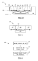
- FIGURE 2C is a cross-sectional view of the package-mounted die of FIGURE 2A through the plane AA';
- FIGURE 3 is an alternate embodiment of a cover plate according to the present invention.
- FIGURE 4 is a flow diagram of a method according to the present invention.
- a MEMS device 22 which may be an accelerometer, a gyroscope, or any other suitable MEMS device, is mounted to a rectangular block die 24 during the MEMS build.
- the die 24 is mounted to a rectangular block cover plate 26 via gold bumps 30 (which can be approximately .001" to .005" in diameter, and the die 24 can be flip-chip mounted to the cover plate 26.
- the gold bumps 30 provide all of the structural strength necessary to prevent dislodging the die 24 during use.
- the MEMS device 22 can be protected from contact during flip-chip mounting using etched features or process controls.
- the cover plate 26 is mounted to a package 28, a rectangular block including a recess 23 (or wirebond shelf) with a step 25, sized and shaped to receive the MEMS device 22, the die 24, and the cover plate 26.
- the cover plate 26 is mounted to the step 25 of the package 28 via gold bumps 32, and the cover plate 26 can be flip-chip mounted to the package 28.
- the package 28 can be a Leadless Ceramic Chip Carrier (LCCC).
- Electrically conductive traces 34 from the MEMS device 22 to the gold bumps 30, and conductive traces 36 from the gold bumps 30 to the gold bumps 32 provide a connection between the MEMS device 22 and the package 28 so that the MEMS device 22 can be in electrical contact with devices or systems (not shown) outside the package as necessary depending on the intended use of the device 22.
- the die 24 has a preselected CTE
- the package 28 has a preselected CTE that is higher than the CTE of the die 24.
- the cover plate 26 is made of the same material as the die 24 with the same CTE as the die 24.
- FIGURE 3 shows a portion of an alternate example not forming part of the present invention.
- the cover plate 26 includes a composite of first and second materials 27,29.
- the die has a first CTE.
- the second material 29 has a CTE greater than the CTE of the die 24 and less than the CTE of the first material 29.
- the first material 27 has a CTE less than the CTE of the package 24.
- the package 24 is attached to the first material 27, and the die is attached to the second material 29.
- FIGURE 4 shows a process flow diagram of a method 40 for creating an example not forming part of the present invention.
- a MEMS device is mounted to a die having a CTE equal or greater than the CTE of the MEMS device.
- the die is mounted to a cover plate having a CTE greater than the CTE of the die and less than the CTE of a package.
- the die is mounted to the package.
- electrically conductive traces 34, 36 electrically connect the MEMS device to the package.
- the traces are mechanically more stable under shock than wirebonds, because they are printed on the package and cover plate.
Landscapes
- Engineering & Computer Science (AREA)
- Microelectronics & Electronic Packaging (AREA)
- Computer Hardware Design (AREA)
- Micromachines (AREA)
- Wire Bonding (AREA)
Claims (4)
- Dispositif (20) comprenant :un dispositif de microsystème électromécanique (MEMS) (22) ;une puce (24) configurée de façon à supporter le dispositif MEMS (22), cette puce ayant un premier côté et un premier coefficient de dilatation thermique ;une plaque-couvercle (26) attachée à la puce (24) cette plaque-couvercle ayant un premier côté et un deuxième coefficient de dilatation thermique ;un boîtier (28) attaché à la plaque-couvercle (26), ce boîtier ayant un troisième coefficient de dilatation thermique ; etun dispositif de fixation électriquement conducteur (30, 32) configuré de façon à attacher la puce à la plaque-couvercle (26) et à attacher la plaque-couvercle (26) au boîtier (28),dans lequel la puce est configurée de façon à supporter le dispositif MEMS (22) sur le premier côté de la puce (24), et le premier côté de la plaque-couvercle (26) est attaché au premier côté de la puce (24) au moyen du dispositif de fixation électriquement conducteur (30, 32), et le premier côté de la plaque-couvercle (26) est aussi monté sur le boîtier (28) au moyen du dispositif de fixation électriquement conducteur (30, 32),dans lequel le dispositif de fixation électriquement conducteur (30, 32) comprend au moins soit des bosses en or, soit des billes de soudure, soit des polymères conducteurs, soit des conducteurs directionnels, etdans lequel la plaque-couvercle (26) est faite du même matériau que la puce (24), ne fournissant ainsi aucune disparité entre les coefficients de dilatation thermique de la plaque-couvercle (26) et de la puce (24).
- Dispositif selon la revendication 1, le boîtier comprenant en outre un évidement dimensionné et formé de façon à recevoir le dispositif MEMS (22), la puce (24) et la plaque-couvercle (26), cet évidement comprenant un gradin.
- Dispositif selon la revendication 2, dans lequel le premier côté de la plaque-couvercle (26) est attaché au gradin du boîtier.
- Dispositif selon la revendication 1, dans lequel le boîtier est soit un porte-puce céramique à souder, soit un porte-puce céramique enfichable, soit un porte-puce plastique enfichable, soit un porte-puce plastique à souder.
Applications Claiming Priority (1)
| Application Number | Priority Date | Filing Date | Title |
|---|---|---|---|
| US11/765,322 US8742557B2 (en) | 2007-06-19 | 2007-06-19 | Die mounting stress isolator |
Publications (3)
| Publication Number | Publication Date |
|---|---|
| EP2006248A2 EP2006248A2 (fr) | 2008-12-24 |
| EP2006248A3 EP2006248A3 (fr) | 2012-06-06 |
| EP2006248B1 true EP2006248B1 (fr) | 2013-09-04 |
Family
ID=39824289
Family Applications (1)
| Application Number | Title | Priority Date | Filing Date |
|---|---|---|---|
| EP08158292.6A Not-in-force EP2006248B1 (fr) | 2007-06-19 | 2008-06-13 | Isolateur de contrainte monté sur une puce |
Country Status (3)
| Country | Link |
|---|---|
| US (1) | US8742557B2 (fr) |
| EP (1) | EP2006248B1 (fr) |
| JP (1) | JP5143640B2 (fr) |
Cited By (1)
| Publication number | Priority date | Publication date | Assignee | Title |
|---|---|---|---|---|
| WO2024008976A1 (fr) | 2022-07-08 | 2024-01-11 | Autorient Technologies AS | Dispositifs micromécaniques ayant une structure de découplage des contraintes et leurs procédés de fabrication |
Families Citing this family (7)
| Publication number | Priority date | Publication date | Assignee | Title |
|---|---|---|---|---|
| US7830003B2 (en) | 2007-12-27 | 2010-11-09 | Honeywell International, Inc. | Mechanical isolation for MEMS devices |
| US11181688B2 (en) | 2009-10-13 | 2021-11-23 | Skorpios Technologies, Inc. | Integration of an unprocessed, direct-bandgap chip into a silicon photonic device |
| US9496431B2 (en) * | 2013-10-09 | 2016-11-15 | Skorpios Technologies, Inc. | Coplanar integration of a direct-bandgap chip into a silicon photonic device |
| DE102015100757B3 (de) * | 2015-01-20 | 2016-06-16 | Epcos Ag | Modul mit spannungsfrei befestigtem MEMS-Bauelement |
| CN112158792B (zh) * | 2020-09-22 | 2024-07-02 | 浙江大学 | 一种适用于mems加速度传感器芯片的低应力封装结构 |
| CN112938888B (zh) * | 2021-02-01 | 2023-06-16 | 南京理工大学 | 具有应力调节的mems传感器芯片封装结构与方法 |
| EP4467512A1 (fr) * | 2023-05-23 | 2024-11-27 | Murata Manufacturing Co., Ltd. | Composant mems avec puce inversée |
Family Cites Families (15)
| Publication number | Priority date | Publication date | Assignee | Title |
|---|---|---|---|---|
| JP3005177B2 (ja) * | 1995-06-27 | 2000-01-31 | 松下電工株式会社 | 半導体パッケージの実装構造 |
| US6573609B2 (en) * | 1997-11-25 | 2003-06-03 | Tessera, Inc. | Microelectronic component with rigid interposer |
| US6281573B1 (en) * | 1998-03-31 | 2001-08-28 | International Business Machines Corporation | Thermal enhancement approach using solder compositions in the liquid state |
| US6384473B1 (en) * | 2000-05-16 | 2002-05-07 | Sandia Corporation | Microelectronic device package with an integral window |
| US6828663B2 (en) * | 2001-03-07 | 2004-12-07 | Teledyne Technologies Incorporated | Method of packaging a device with a lead frame, and an apparatus formed therefrom |
| JP2004087700A (ja) * | 2002-08-26 | 2004-03-18 | Nec Semiconductors Kyushu Ltd | 半導体装置およびその製造方法 |
| US20040046248A1 (en) | 2002-09-05 | 2004-03-11 | Corning Intellisense Corporation | Microsystem packaging and associated methods |
| US7060601B2 (en) * | 2003-12-17 | 2006-06-13 | Tru-Si Technologies, Inc. | Packaging substrates for integrated circuits and soldering methods |
| US20050205951A1 (en) * | 2004-03-18 | 2005-09-22 | Honeywell Internatioanl, Inc. | Flip chip bonded micro-electromechanical system (MEMS) device |
| EP1738411A4 (fr) * | 2004-04-22 | 2012-06-27 | Panasonic Corp | Dispositif de capteur, système de capteur et procédés de fabrication de ceux-ci |
| JP4969822B2 (ja) * | 2004-12-06 | 2012-07-04 | 株式会社デンソー | センサ装置 |
| US7202560B2 (en) * | 2004-12-15 | 2007-04-10 | Avago Technologies Wireless Ip (Singapore) Pte. Ltd. | Wafer bonding of micro-electro mechanical systems to active circuitry |
| US7491567B2 (en) * | 2005-11-22 | 2009-02-17 | Honeywell International Inc. | MEMS device packaging methods |
| JP5107539B2 (ja) * | 2006-08-03 | 2012-12-26 | 新光電気工業株式会社 | 半導体装置および半導体装置の製造方法 |
| JP2008244244A (ja) * | 2007-03-28 | 2008-10-09 | Sony Corp | 電気機械装置および電気・電子機器 |
-
2007
- 2007-06-19 US US11/765,322 patent/US8742557B2/en active Active
-
2008
- 2008-06-13 EP EP08158292.6A patent/EP2006248B1/fr not_active Not-in-force
- 2008-06-18 JP JP2008159047A patent/JP5143640B2/ja not_active Expired - Fee Related
Cited By (1)
| Publication number | Priority date | Publication date | Assignee | Title |
|---|---|---|---|---|
| WO2024008976A1 (fr) | 2022-07-08 | 2024-01-11 | Autorient Technologies AS | Dispositifs micromécaniques ayant une structure de découplage des contraintes et leurs procédés de fabrication |
Also Published As
| Publication number | Publication date |
|---|---|
| EP2006248A3 (fr) | 2012-06-06 |
| EP2006248A2 (fr) | 2008-12-24 |
| US20080315397A1 (en) | 2008-12-25 |
| JP2009021583A (ja) | 2009-01-29 |
| US8742557B2 (en) | 2014-06-03 |
| JP5143640B2 (ja) | 2013-02-13 |
Similar Documents
| Publication | Publication Date | Title |
|---|---|---|
| US7419853B2 (en) | Method of fabrication for chip scale package for a micro component | |
| EP1886969B1 (fr) | Procédés pour la fabrication d'encapsulations sous vide de dispositifs sur wafer | |
| US6982491B1 (en) | Sensor semiconductor package and method of manufacturing the same | |
| US7571647B2 (en) | Package structure for an acceleration sensor | |
| EP1192419B1 (fr) | Ensemble et encapsulation de detecteur integre et a axe multiple | |
| EP2006248A2 (fr) | Isolateur de contrainte monté sur une puce | |
| EP2388816A1 (fr) | Dispositif de capteur semi-conducteur, procédé de fabrication du dispositif de capteur semi-conducteur, boîtier, procédé de fabrication du boîtier, module, procédé de fabrication du module, et dispositif électronique | |
| US20100258950A1 (en) | Package with semiconductor device and integrated circuit mounted therein and method for manufacturing such package | |
| CN101958256B (zh) | 垂直传感器组装方法 | |
| US6750521B1 (en) | Surface mount package for a micromachined device | |
| US20050279166A1 (en) | Semiconductor acceleration sensor device and method for manufacturing the same | |
| EP2112489A2 (fr) | Capteur de pression, son procédé de fabrication et composant électronique correspondant | |
| WO2014117119A1 (fr) | Boîtier de semi-conducteur basé sur une grille de connexion ayant des bornes sur des surfaces supérieure et inférieure | |
| JP5978170B2 (ja) | トランスファーモールド型センサ装置 | |
| EP2048109A2 (fr) | Dispositif électronique, module électronique, et leurs procédés de fabrication | |
| EP2840375A1 (fr) | Dispositif avec structure micro ou nanométrique | |
| KR20050095586A (ko) | 전자 장치, 그 제조 방법 및 이용법 | |
| JP2009241164A (ja) | 半導体センサー装置およびその製造方法 | |
| KR20070036668A (ko) | 반도체 장치 | |
| JP5052459B2 (ja) | 半導体センサー装置 | |
| US8097950B2 (en) | Semiconductor device and electronic component module using the same | |
| EP3680211A1 (fr) | Unité de capteur et procédé d'interconnexion d'un substrat et d'un support | |
| US7037805B2 (en) | Methods and apparatus for attaching a die to a substrate | |
| US20100255622A1 (en) | Systems and methods for affixing a silicon device to a support structure | |
| EP1837303A1 (fr) | Socle intégré pour monter une structure MEMS |
Legal Events
| Date | Code | Title | Description |
|---|---|---|---|
| PUAI | Public reference made under article 153(3) epc to a published international application that has entered the european phase |
Free format text: ORIGINAL CODE: 0009012 |
|
| 17P | Request for examination filed |
Effective date: 20080613 |
|
| AK | Designated contracting states |
Kind code of ref document: A2 Designated state(s): AT BE BG CH CY CZ DE DK EE ES FI FR GB GR HR HU IE IS IT LI LT LU LV MC MT NL NO PL PT RO SE SI SK TR |
|
| AX | Request for extension of the european patent |
Extension state: AL BA MK RS |
|
| PUAL | Search report despatched |
Free format text: ORIGINAL CODE: 0009013 |
|
| AK | Designated contracting states |
Kind code of ref document: A3 Designated state(s): AT BE BG CH CY CZ DE DK EE ES FI FR GB GR HR HU IE IS IT LI LT LU LV MC MT NL NO PL PT RO SE SI SK TR |
|
| AX | Request for extension of the european patent |
Extension state: AL BA MK RS |
|
| RIC1 | Information provided on ipc code assigned before grant |
Ipc: B81B 7/00 20060101AFI20120503BHEP |
|
| 17Q | First examination report despatched |
Effective date: 20120504 |
|
| AKX | Designation fees paid |
Designated state(s): CH DE FR LI |
|
| GRAP | Despatch of communication of intention to grant a patent |
Free format text: ORIGINAL CODE: EPIDOSNIGR1 |
|
| INTG | Intention to grant announced |
Effective date: 20130423 |
|
| GRAS | Grant fee paid |
Free format text: ORIGINAL CODE: EPIDOSNIGR3 |
|
| GRAA | (expected) grant |
Free format text: ORIGINAL CODE: 0009210 |
|
| AK | Designated contracting states |
Kind code of ref document: B1 Designated state(s): CH DE FR LI |
|
| REG | Reference to a national code |
Ref country code: CH Ref legal event code: EP |
|
| REG | Reference to a national code |
Ref country code: DE Ref legal event code: R096 Ref document number: 602008027254 Country of ref document: DE Effective date: 20131031 |
|
| REG | Reference to a national code |
Ref country code: DE Ref legal event code: R097 Ref document number: 602008027254 Country of ref document: DE |
|
| PLBE | No opposition filed within time limit |
Free format text: ORIGINAL CODE: 0009261 |
|
| STAA | Information on the status of an ep patent application or granted ep patent |
Free format text: STATUS: NO OPPOSITION FILED WITHIN TIME LIMIT |
|
| 26N | No opposition filed |
Effective date: 20140605 |
|
| REG | Reference to a national code |
Ref country code: DE Ref legal event code: R097 Ref document number: 602008027254 Country of ref document: DE Effective date: 20140605 |
|
| REG | Reference to a national code |
Ref country code: FR Ref legal event code: PLFP Year of fee payment: 8 |
|
| PGFP | Annual fee paid to national office [announced via postgrant information from national office to epo] |
Ref country code: FR Payment date: 20150528 Year of fee payment: 8 |
|
| REG | Reference to a national code |
Ref country code: FR Ref legal event code: ST Effective date: 20170228 |
|
| PG25 | Lapsed in a contracting state [announced via postgrant information from national office to epo] |
Ref country code: FR Free format text: LAPSE BECAUSE OF NON-PAYMENT OF DUE FEES Effective date: 20160630 |
|
| PGFP | Annual fee paid to national office [announced via postgrant information from national office to epo] |
Ref country code: DE Payment date: 20180831 Year of fee payment: 11 |
|
| PGFP | Annual fee paid to national office [announced via postgrant information from national office to epo] |
Ref country code: CH Payment date: 20180705 Year of fee payment: 11 |
|
| REG | Reference to a national code |
Ref country code: DE Ref legal event code: R119 Ref document number: 602008027254 Country of ref document: DE |
|
| REG | Reference to a national code |
Ref country code: CH Ref legal event code: PL |
|
| PG25 | Lapsed in a contracting state [announced via postgrant information from national office to epo] |
Ref country code: DE Free format text: LAPSE BECAUSE OF NON-PAYMENT OF DUE FEES Effective date: 20200101 |
|
| PG25 | Lapsed in a contracting state [announced via postgrant information from national office to epo] |
Ref country code: LI Free format text: LAPSE BECAUSE OF NON-PAYMENT OF DUE FEES Effective date: 20190630 Ref country code: CH Free format text: LAPSE BECAUSE OF NON-PAYMENT OF DUE FEES Effective date: 20190630 |
|
| P01 | Opt-out of the competence of the unified patent court (upc) registered |
Effective date: 20230525 |