EP2006249A2 - Gravure plasma haute résolution - Google Patents
Gravure plasma haute résolution Download PDFInfo
- Publication number
- EP2006249A2 EP2006249A2 EP08158646A EP08158646A EP2006249A2 EP 2006249 A2 EP2006249 A2 EP 2006249A2 EP 08158646 A EP08158646 A EP 08158646A EP 08158646 A EP08158646 A EP 08158646A EP 2006249 A2 EP2006249 A2 EP 2006249A2
- Authority
- EP
- European Patent Office
- Prior art keywords
- substrate
- directing
- ion
- plasma
- portions
- Prior art date
- Legal status (The legal status is an assumption and is not a legal conclusion. Google has not performed a legal analysis and makes no representation as to the accuracy of the status listed.)
- Ceased
Links
- 238000000034 method Methods 0.000 claims abstract description 77
- 239000000758 substrate Substances 0.000 claims abstract description 56
- 230000008569 process Effects 0.000 claims abstract description 41
- 238000005530 etching Methods 0.000 claims abstract description 30
- 230000001681 protective effect Effects 0.000 claims abstract description 25
- 239000002243 precursor Substances 0.000 claims abstract description 19
- 238000010894 electron beam technology Methods 0.000 claims abstract description 17
- 238000010884 ion-beam technique Methods 0.000 claims abstract description 16
- 239000000463 material Substances 0.000 claims description 47
- 150000002500 ions Chemical class 0.000 claims description 44
- 239000002245 particle Substances 0.000 claims description 29
- 238000000151 deposition Methods 0.000 claims description 23
- 230000000873 masking effect Effects 0.000 claims description 11
- 230000007935 neutral effect Effects 0.000 claims description 10
- 230000003287 optical effect Effects 0.000 claims description 8
- 239000011241 protective layer Substances 0.000 claims description 8
- 238000009616 inductively coupled plasma Methods 0.000 claims description 6
- 239000010410 layer Substances 0.000 claims description 6
- 238000003486 chemical etching Methods 0.000 claims description 5
- 238000006243 chemical reaction Methods 0.000 claims description 5
- 238000004544 sputter deposition Methods 0.000 claims description 5
- 238000010494 dissociation reaction Methods 0.000 claims description 3
- 230000005593 dissociations Effects 0.000 claims description 3
- 230000004907 flux Effects 0.000 claims description 3
- 230000001939 inductive effect Effects 0.000 claims description 2
- 238000002347 injection Methods 0.000 claims description 2
- 239000007924 injection Substances 0.000 claims description 2
- 230000003116 impacting effect Effects 0.000 claims 1
- 238000000059 patterning Methods 0.000 claims 1
- 238000004519 manufacturing process Methods 0.000 abstract description 7
- 238000000354 decomposition reaction Methods 0.000 abstract 1
- 239000007789 gas Substances 0.000 description 27
- 230000008021 deposition Effects 0.000 description 18
- WFKWXMTUELFFGS-UHFFFAOYSA-N tungsten Chemical compound [W] WFKWXMTUELFFGS-UHFFFAOYSA-N 0.000 description 8
- 229910052721 tungsten Inorganic materials 0.000 description 8
- 239000010937 tungsten Substances 0.000 description 8
- 235000012431 wafers Nutrition 0.000 description 7
- IGELFKKMDLGCJO-UHFFFAOYSA-N xenon difluoride Chemical compound F[Xe]F IGELFKKMDLGCJO-UHFFFAOYSA-N 0.000 description 7
- XKRFYHLGVUSROY-UHFFFAOYSA-N Argon Chemical compound [Ar] XKRFYHLGVUSROY-UHFFFAOYSA-N 0.000 description 6
- 229920002120 photoresistant polymer Polymers 0.000 description 6
- VYPSYNLAJGMNEJ-UHFFFAOYSA-N Silicium dioxide Chemical compound O=[Si]=O VYPSYNLAJGMNEJ-UHFFFAOYSA-N 0.000 description 5
- 239000001301 oxygen Substances 0.000 description 5
- 229910052760 oxygen Inorganic materials 0.000 description 5
- XUIMIQQOPSSXEZ-UHFFFAOYSA-N Silicon Chemical compound [Si] XUIMIQQOPSSXEZ-UHFFFAOYSA-N 0.000 description 4
- QVGXLLKOCUKJST-UHFFFAOYSA-N atomic oxygen Chemical compound [O] QVGXLLKOCUKJST-UHFFFAOYSA-N 0.000 description 4
- -1 for example Chemical class 0.000 description 4
- 229910052710 silicon Inorganic materials 0.000 description 4
- 239000010703 silicon Substances 0.000 description 4
- 229910052786 argon Inorganic materials 0.000 description 3
- 238000005137 deposition process Methods 0.000 description 3
- 230000008439 repair process Effects 0.000 description 3
- 239000000126 substance Substances 0.000 description 3
- OKTJSMMVPCPJKN-UHFFFAOYSA-N Carbon Chemical compound [C] OKTJSMMVPCPJKN-UHFFFAOYSA-N 0.000 description 2
- PPBRXRYQALVLMV-UHFFFAOYSA-N Styrene Chemical compound C=CC1=CC=CC=C1 PPBRXRYQALVLMV-UHFFFAOYSA-N 0.000 description 2
- BOTDANWDWHJENH-UHFFFAOYSA-N Tetraethyl orthosilicate Chemical compound CCO[Si](OCC)(OCC)OCC BOTDANWDWHJENH-UHFFFAOYSA-N 0.000 description 2
- 239000006227 byproduct Substances 0.000 description 2
- 229910052799 carbon Inorganic materials 0.000 description 2
- 229910052681 coesite Inorganic materials 0.000 description 2
- 229910052906 cristobalite Inorganic materials 0.000 description 2
- 238000000313 electron-beam-induced deposition Methods 0.000 description 2
- 229910001338 liquidmetal Inorganic materials 0.000 description 2
- 238000001459 lithography Methods 0.000 description 2
- 238000003754 machining Methods 0.000 description 2
- 229910052751 metal Inorganic materials 0.000 description 2
- 239000002184 metal Substances 0.000 description 2
- 239000000203 mixture Substances 0.000 description 2
- 238000012986 modification Methods 0.000 description 2
- 230000004048 modification Effects 0.000 description 2
- 238000000206 photolithography Methods 0.000 description 2
- BASFCYQUMIYNBI-UHFFFAOYSA-N platinum Substances [Pt] BASFCYQUMIYNBI-UHFFFAOYSA-N 0.000 description 2
- 230000005855 radiation Effects 0.000 description 2
- 239000004065 semiconductor Substances 0.000 description 2
- 239000000377 silicon dioxide Substances 0.000 description 2
- 229910052682 stishovite Inorganic materials 0.000 description 2
- 229910052905 tridymite Inorganic materials 0.000 description 2
- NXHILIPIEUBEPD-UHFFFAOYSA-H tungsten hexafluoride Chemical compound F[W](F)(F)(F)(F)F NXHILIPIEUBEPD-UHFFFAOYSA-H 0.000 description 2
- XMWRBQBLMFGWIX-UHFFFAOYSA-N C60 fullerene Chemical class C12=C3C(C4=C56)=C7C8=C5C5=C9C%10=C6C6=C4C1=C1C4=C6C6=C%10C%10=C9C9=C%11C5=C8C5=C8C7=C3C3=C7C2=C1C1=C2C4=C6C4=C%10C6=C9C9=C%11C5=C5C8=C3C3=C7C1=C1C2=C4C6=C2C9=C5C3=C12 XMWRBQBLMFGWIX-UHFFFAOYSA-N 0.000 description 1
- MYMOFIZGZYHOMD-UHFFFAOYSA-N Dioxygen Chemical compound O=O MYMOFIZGZYHOMD-UHFFFAOYSA-N 0.000 description 1
- 229910008940 W(CO)6 Inorganic materials 0.000 description 1
- 239000002156 adsorbate Substances 0.000 description 1
- 230000004075 alteration Effects 0.000 description 1
- 230000005540 biological transmission Effects 0.000 description 1
- FQNHWXHRAUXLFU-UHFFFAOYSA-N carbon monoxide;tungsten Chemical group [W].[O+]#[C-].[O+]#[C-].[O+]#[C-].[O+]#[C-].[O+]#[C-].[O+]#[C-] FQNHWXHRAUXLFU-UHFFFAOYSA-N 0.000 description 1
- 238000005266 casting Methods 0.000 description 1
- 238000005229 chemical vapour deposition Methods 0.000 description 1
- 239000011248 coating agent Substances 0.000 description 1
- 238000000576 coating method Methods 0.000 description 1
- 150000001875 compounds Chemical class 0.000 description 1
- 238000009792 diffusion process Methods 0.000 description 1
- 230000009977 dual effect Effects 0.000 description 1
- 230000000694 effects Effects 0.000 description 1
- 238000005516 engineering process Methods 0.000 description 1
- 229910003472 fullerene Inorganic materials 0.000 description 1
- 229910052733 gallium Inorganic materials 0.000 description 1
- CKHJYUSOUQDYEN-UHFFFAOYSA-N gallium(3+) Chemical compound [Ga+3] CKHJYUSOUQDYEN-UHFFFAOYSA-N 0.000 description 1
- 238000003384 imaging method Methods 0.000 description 1
- 238000007689 inspection Methods 0.000 description 1
- 238000003913 materials processing Methods 0.000 description 1
- 230000001404 mediated effect Effects 0.000 description 1
- 239000007769 metal material Substances 0.000 description 1
- 150000002739 metals Chemical class 0.000 description 1
- 238000005459 micromachining Methods 0.000 description 1
- 238000003801 milling Methods 0.000 description 1
- 239000002086 nanomaterial Substances 0.000 description 1
- 238000005240 physical vapour deposition Methods 0.000 description 1
- 238000000623 plasma-assisted chemical vapour deposition Methods 0.000 description 1
- VJGYJQUTDBRHBS-UHFFFAOYSA-N platinum;trifluorophosphane Chemical compound [Pt].FP(F)F.FP(F)F.FP(F)F.FP(F)F VJGYJQUTDBRHBS-UHFFFAOYSA-N 0.000 description 1
- 238000005498 polishing Methods 0.000 description 1
- 230000002265 prevention Effects 0.000 description 1
- 239000000047 product Substances 0.000 description 1
- 239000011253 protective coating Substances 0.000 description 1
- 238000005086 pumping Methods 0.000 description 1
- 238000000926 separation method Methods 0.000 description 1
- 229910052814 silicon oxide Inorganic materials 0.000 description 1
- 238000006467 substitution reaction Methods 0.000 description 1
Images
Classifications
-
- B—PERFORMING OPERATIONS; TRANSPORTING
- B05—SPRAYING OR ATOMISING IN GENERAL; APPLYING FLUENT MATERIALS TO SURFACES, IN GENERAL
- B05C—APPARATUS FOR APPLYING FLUENT MATERIALS TO SURFACES, IN GENERAL
- B05C21/00—Accessories or implements for use in connection with applying liquids or other fluent materials to surfaces, not provided for in groups B05C1/00 - B05C19/00
- B05C21/005—Masking devices
-
- B—PERFORMING OPERATIONS; TRANSPORTING
- B81—MICROSTRUCTURAL TECHNOLOGY
- B81C—PROCESSES OR APPARATUS SPECIALLY ADAPTED FOR THE MANUFACTURE OR TREATMENT OF MICROSTRUCTURAL DEVICES OR SYSTEMS
- B81C1/00—Manufacture or treatment of devices or systems in or on a substrate
- B81C1/00436—Shaping materials, i.e. techniques for structuring the substrate or the layers on the substrate
- B81C1/00523—Etching material
- B81C1/00531—Dry etching
-
- H—ELECTRICITY
- H01—ELECTRIC ELEMENTS
- H01J—ELECTRIC DISCHARGE TUBES OR DISCHARGE LAMPS
- H01J37/00—Discharge tubes with provision for introducing objects or material to be exposed to the discharge, e.g. for the purpose of examination or processing thereof
- H01J37/30—Electron-beam or ion-beam tubes for localised treatment of objects
- H01J37/305—Electron-beam or ion-beam tubes for localised treatment of objects for casting, melting, evaporating, or etching
- H01J37/3053—Electron-beam or ion-beam tubes for localised treatment of objects for casting, melting, evaporating, or etching for evaporating or etching
-
- H—ELECTRICITY
- H01—ELECTRIC ELEMENTS
- H01J—ELECTRIC DISCHARGE TUBES OR DISCHARGE LAMPS
- H01J37/00—Discharge tubes with provision for introducing objects or material to be exposed to the discharge, e.g. for the purpose of examination or processing thereof
- H01J37/30—Electron-beam or ion-beam tubes for localised treatment of objects
- H01J37/317—Electron-beam or ion-beam tubes for localised treatment of objects for changing properties of the objects or for applying thin layers thereon, e.g. for ion implantation
-
- B—PERFORMING OPERATIONS; TRANSPORTING
- B81—MICROSTRUCTURAL TECHNOLOGY
- B81C—PROCESSES OR APPARATUS SPECIALLY ADAPTED FOR THE MANUFACTURE OR TREATMENT OF MICROSTRUCTURAL DEVICES OR SYSTEMS
- B81C2201/00—Manufacture or treatment of microstructural devices or systems
- B81C2201/01—Manufacture or treatment of microstructural devices or systems in or on a substrate
- B81C2201/0101—Shaping material; Structuring the bulk substrate or layers on the substrate; Film patterning
- B81C2201/0128—Processes for removing material
- B81C2201/013—Etching
- B81C2201/0132—Dry etching, i.e. plasma etching, barrel etching, reactive ion etching [RIE], sputter etching or ion milling
-
- B—PERFORMING OPERATIONS; TRANSPORTING
- B81—MICROSTRUCTURAL TECHNOLOGY
- B81C—PROCESSES OR APPARATUS SPECIALLY ADAPTED FOR THE MANUFACTURE OR TREATMENT OF MICROSTRUCTURAL DEVICES OR SYSTEMS
- B81C2201/00—Manufacture or treatment of microstructural devices or systems
- B81C2201/01—Manufacture or treatment of microstructural devices or systems in or on a substrate
- B81C2201/0101—Shaping material; Structuring the bulk substrate or layers on the substrate; Film patterning
- B81C2201/0128—Processes for removing material
- B81C2201/0143—Focussed beam, i.e. laser, ion or e-beam
-
- H—ELECTRICITY
- H01—ELECTRIC ELEMENTS
- H01J—ELECTRIC DISCHARGE TUBES OR DISCHARGE LAMPS
- H01J2237/00—Discharge tubes exposing object to beam, e.g. for analysis treatment, etching, imaging
- H01J2237/30—Electron or ion beam tubes for processing objects
- H01J2237/317—Processing objects on a microscale
- H01J2237/3174—Etching microareas
-
- H—ELECTRICITY
- H01—ELECTRIC ELEMENTS
- H01J—ELECTRIC DISCHARGE TUBES OR DISCHARGE LAMPS
- H01J2237/00—Discharge tubes exposing object to beam, e.g. for analysis treatment, etching, imaging
- H01J2237/30—Electron or ion beam tubes for processing objects
- H01J2237/317—Processing objects on a microscale
- H01J2237/3174—Etching microareas
- H01J2237/31742—Etching microareas for repairing masks
- H01J2237/31744—Etching microareas for repairing masks introducing gas in vicinity of workpiece
-
- H—ELECTRICITY
- H01—ELECTRIC ELEMENTS
- H01J—ELECTRIC DISCHARGE TUBES OR DISCHARGE LAMPS
- H01J2237/00—Discharge tubes exposing object to beam, e.g. for analysis treatment, etching, imaging
- H01J2237/30—Electron or ion beam tubes for processing objects
- H01J2237/317—Processing objects on a microscale
- H01J2237/31749—Focused ion beam
Definitions
- the present invention relates to materials processing on a microscopic scale.
- a typical photolithography technique involves depositing a thin layer of a photosensitive material called a "photoresist" onto the surface of a semiconductor substrate such as a silicon wafer, by a process called “casting.”
- Photolithographic imaging is then used to transfer a desired pattern, designed on a photolithographic mask, to the photoresist by selective exposure to a radiation source such as light.
- the photoresist is then chemically developed to remove the radiation exposed areas (in a positive resist) or the unexposed areas (in a negative resist), leaving behind a pattern of photoresist to protect specific parts of the substrate during subsequent processes such as etching (removing material), deposition (adding material to the substrate surface), or diffusion (diffusing atoms into the substrate).
- Etching can be performed, for example, using a reactive chemical, sometimes in the form of a plasma.
- a plasma can also be used to sputter material from a surface by causing charged particles from the plasma to impact the surface with sufficient momentum to displace surface molecules.
- Deposition can be performed, for example, by chemical or physical vapor deposition or plasma enhanced chemical vapor deposition. After processing, the patterned photoresist is removed. Lithography process are time consuming and, while efficient for processing a complete wafer, are less useful for localized processing.
- Focused beams such as focused ion beams (FIBs), electron beams, and laser beams, are also used for forming small structures. While being able to form extremely precise structures, processing by such beams is typically too slow to be used for mass production of fine structures.
- FIBs can be used to sputter a substrate surface because they employ a relatively large ion such as, for example, a gallium ion (Ga + ) that can be accelerated easily to achieve the momentum needed to displace molecules of the substrate.
- FIBs can also be used with a precursor gas to enhance etching chemically or to deposit a material onto the surface.
- Electron beams can also be used, together with an assisting precursor gas, to give rise to etching or deposition processes.
- Electron beam, FIB, reactive gasses and plasma processes can be used either alone or in combination with one another to manipulate substrate surfaces, for example, to create and repair photolithographic masks. Reactive gasses typically also exhibit material selectivity. These processes can provide varying degrees of fabrication tolerances, material characteristics, processing times and machining flexibility.
- An object of the invention is to provide a method and apparatus for fabricating structures on the micro and nano scales.
- the present invention includes creating a protective coating upon portions of a substrate preferably using a focused beam process and then etching unmasked substrate portions using a material selective plasma beam formed using an ion focusing column positioned between a plasma chamber and the substrate.
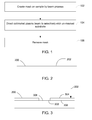
- FIG. 1 is a flowchart showing the preferred order of processing of the present invention.
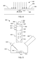
- FIG. 2 shows schematically an elevated side view of a substrate sample having an upper surface
- FIG. 3 shows schematically the substrate of FIG.2 further showing portions of a protective mask upon the surface
- FIG. 4 shows schematically a collimated plasma beam selectively etching an unprotected portion of the substrate of FIGS. 2 and 3 ;
- FIG. 5 shows schematically a dual beam system comprising an electron column, and the combination of a plasma chamber and a differentially pumped ion focusing column for the generation of a plasma beam
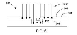
- FIG. 6 shows schematically the selective etching of the protective mask of FIGS. 2 and 3 .
- Preferred embodiments of the invention relate to a method for fabricating nanoscopic and microscopic structures, such as integrated circuits or micro-electromechanical systems, by a beam used to locally fabricate a protective mask, followed by use of a plasma beam etch process.
- beam processes as used in preferred embodiments of the present invention create precisely defined protective mask patterns on a substrate surface and, when followed by etching using a plasma beam, contribute to superior structural tolerances and machining flexibility.
- beam deposition can produce surface features such as line widths of less than about 10 nm.
- FIG. 1 is a flowchart that shows a preferred order of steps of a method of the present invention.
- FIGS. 2 through 4 and FIG. 6 illustrate the various stages of processing of a substrate in accordance with the method shown in FIG. 1.
- FIG. 2 shows a sample substrate 200 having a surface 202 before processing begins.
- a focused beam (e.g., with a beam diameter in the range of 1 nm to 100 ⁇ m, and more commonly in the range of 1 nm to 10 nm) is used to fabricate a protective layer to mask a portion of the substrate surface to protect the masked portion during a subsequent etching step.
- the beam can be used to deposit a masking material using beam-assisted deposition, or the beam can be used to etch a pattern in a layer of mask material previously deposited by other known methods.
- the beam is used to deposit a material that will coordinate with the subsequent etching step insofar the deposited material is etched less by the subsequent process than the exposed or un-masked surface of the substrate material.
- Beam processes such as those used in preferred step 102 typically produce higher definition protective layers than are available through photolithographic means. Furthermore, beam processes are able to process arbitrary regions of a substrate immediately after inspection using the focused beam, without the need to fabricate conventional photolithographic masks. This makes beam processes particularly useful for one-off modifications such as those encountered in photolithographic mask repair, circuit edit, and nanostructure prototyping. Beam processes are, in general, especially suited to localized deposition, by which is meant deposition on a portion of the substrate that is significantly smaller than the entire substrate.
- FIG. 3 shows using a beam 302 to deposit a protective layer or mask 304 upon one or more portions 306 of the surface 202, leaving behind an unmasked region 308 to be processed by a plasma beam as will be better understood further herein.
- beam 302 comprises a charged particle beam, such as an electron beam.
- a method for electron beam deposition is described, for example, in U.S. Pat. No. 6,753,538 to Musil, et al . entitled "Electron Beam Processing.” Musil describes using an electron beam to deposit material by inducing a chemical reaction in a precursor gas that decomposes in the presence of the electron beam to leave an appropriate material on a surface.
- Precursor gases that result in the deposition of an oxide layer include, for example, TEOS (tetraethylorthosilicate), which deposits a silicon oxide protective mask.
- TEOS tetraethylorthosilicate
- Other precursors for electron beam deposition are known and can be used as well. Examples include perdeuterated gallium azide (D 2 GaN 3 ) and Pt(PF 3 ) 4 (tetrakis (trifluorophosphane) platinum) for the deposition of masks rich in GaN and P
- deposition can be done across a range of electron beam energies and currents, depending on the deposition rate and resolution required.
- high beam current and low beam energy result in higher deposition rates, with an optimum beam energy of about 100 eV.
- energies below this value typically result in lower deposition rates.
- higher beam energies are typically required to give a smaller electron beam. Therefore, energies might reasonably range from about 1 keV to about 30 keV with conventional scanning electron microscopes (SEMs) such as, those available from FEI Company, the assignee of the present invention.
- SEMs scanning electron microscopes
- TEMs transmission electron microscopes
- Preferred beam currents range from picoamps to nanoamps. However, there could be applications, for example, in some MEMS fabrication, where much higher currents in the microamp range are preferred when very high deposition rates are required and low resolution is acceptable.
- Typical electron beam spot sizes can range from 1 nm to 100 nm, while spot sizes ranging from 0.1 nm to 10 ⁇ m may be useful in some applications, spanning TEM systems and very high electron current SEM columns.
- the beam 302 used to deposit material forming the protective mask 304 may be a FIB.
- a gas is directed toward a surface and a finely focused ion beam (typically comprising gallium ions), decomposes the gas molecules absorbed on the target surface and causes the metal products to become deposited.
- a finely focused ion beam typically comprising gallium ions
- a process for depositing metal material using a FIB is described in, for example, U.S. Pat. No. 4,609,809 to Yamaguchi, et al . for "Method And Apparatus For Correcting Delicate Wiring of IC Device," which describes the use of a tungsten precursor gas compound in the presence of the FIB to deposit tungsten upon a substrate surface.
- FIB FIB
- FIB FIB
- Other precursor gasses that decompose in the presence of a FIB to deposit a material and can be used with the invention are described, for example, in Handbook of Charged Particle Beam Optics, Ed. Jon Orloff, CRC Press (1997).
- the ion beam can be focused to a point or shaped, as described for example, in U.S. Pat. No. 6,977,386 for "Angular Aperture Shaped Beam System and Method" to Gerlach et al., which patent is assigned to the assignee of the present invention.
- the tern "focused beam" as used herein includes a shaped beam.
- Laser-beam-induced deposition can also be used.
- the beam can deposit material by providing energy to decompose a precursor as described above, or the beam can be comprised include particles, such as fullerenes, that are deposited onto the surface, as described in, for example, U.S.. Pat. App. No. 11/590,570 for "Charged-Particle Beam Processing Using a Cluster Source.”
- the methods of deposition, and the material deposited are preferably such that the resulting protective mask 304 can be selectively removed in a subsequent mask-removal step, as will be described below.
- the mask can also be created by coating the area of interest with a layer of masking material, and then using the beam to remove material from the masking layer to form a desired pattern.
- FIG. 1 shows that the second step 104 comprises directing a first collimated plasma beam toward the substrate surface, the beam selectively etching the substrate surface that is not covered by the mask at a significantly higher rate than it etches the protective mask.
- the first plasma beam 402 exhibits a selective characteristic so that the unmasked material is preferably etched at a rate that is at least two times greater than the etch rate of the protective mask 304 material, more preferably five times greater, even more preferably ten times greater, and most preferably one hundred times greater.
- a first collimated plasma beam 402 is directed toward the surface 202 of the substrate sample 200 to etch the un-masked (unprotected) region.
- the preferred degree of collimation depends on the desired properties of the etched feature and the desired size of the beam. A more highly collimated beam produced more vertical sidewalls in the etched feature. The degree of collimation also affects the beam spot size.
- the first plasma beam 402 is preferably collimated and substantially unfocused, such that the beam spot area is preferably greater than the unmasked area of the substrate surface, but smaller than the area of the mask, That is, the plasma beam is preferably sufficiently broad to etch the entire unmasked region 308, although the plasma beam or sample can be moved to scan and etch all required regions in some embodiments.
- the plasma beam preferably has a constant ion flux profile across the entire unmasked etch region 308 to etch the area evenly.
- the ion flux is preferably constant to within about 20% across the unmasked area of the substrate surface, more preferably to within about 1%, even more preferably to within about 0.1% and most even preferably to within about 0.001 %.
- Plasma beam 402 is local, that is, it covers an area that is significantly smaller that the entire sample. When used to etch high aspect ratio holes, plasma beam 402 is preferably highly collimated to avoid tapering the etching of the holes. In forming some features, such as low aspect ratio holes, collimation is less important.
- the first plasma beam 402 preferably has sufficiently high energy to cause ions in the plasma beam to dissociate upon contact with the surface 202, and sufficiently low energy to prevent significant sputtering of the surface 202. That is, rather than material being removed by momentum transfer from the ions of the plasma beam to the surface, material in unmasked region 308 is removed primarily by a chemical reaction between a reactive molecule formed by the dissociation of ions in the plasma beam upon contact with the sample surface, the chemical reaction forming a volatile byproduct that is evacuated from the vacuum chamber.
- the energy of the ionized particles is preferably such that the material removal rate caused by sputtering is at least five times lower than that caused by chemical etching, preferably 10 times lower, more preferably 100 times lower, and most preferably 1000 times lower.
- the selectivity is such that the mask is preferably not completely removed when the etching process is completed, or at least the mask is in place long enough that the masked area is subject to an acceptable amount of etching.
- the combination of ion dissociation and sputter prevention is achieved by fine-tuning the ion landing energy at the surface. Typical energies lie in the range of 1 eV and 10 keV, and more preferably in the range of 10 eV and 500 eV.
- the ions from the plasma disassociate on contact with the surface 202 and etch the protective mask 304 little or not at all, while etching primarily the un-masked region 308.
- Reactive plasma precursors that may be used include, for example, SF 6 and XeF 2 , which can be used to form plasma beams comprising, for example, SF 6 + and XeF 2 + , respectively.
- FIG. 4 shows plasma beam 402 in the process of forming a trench 410 having sidewalls 412. It will be appreciated by those of ordinary skill in the art that the plasma etch process described above will tend to etch high aspect ratio trenches with significantly parallel sidewalls. This is so because (i) the plasma beam is collimated, (ii) the volatile byproducts do not re-deposit onto the pit sidewalls, and (iii) neutral gas molecules are reduced or eliminated inside the chamber containing the sample 200 by having the sample 200 positioned outside the plasma chamber. The last point is significant because the plasma beam gives rise to secondary electron emission from the sample.
- Said electrons can impact sidewalls 412, where they can dissociate adsorbed etch precursor gas molecules, giving rise to (typically undesired) lateral etching of the sidewalls.
- Such lateral etching is absent when neutral etch precursor molecules are not present inside the specimen chamber.
- neutral gas molecules diffuse into the plasma beam focusing column and the specimen chamber.
- the neutral molecules can be prevented from entering the specimen chamber by the employment of a differentially pumped plasma focusing column.
- FIG. 5 shows schematically a dual-beam system 500 implementation of the present invention.
- System 500 includes an ion beam column 502 and an electron beam column 504. While ion beam column 502 is shown vertically oriented and electron beam column 504 is shown oriented at an angle to vertical, other embodiments may employ a vertical electron beam column 504 and a tilted ion beam column 502.
- Ion beam column 502 includes a plasma chamber 504 which is supplied with a gas or gasses through a gas inlet 506.
- Plasma chamber 504 can use, for example, an inductively coupled, magnetically enhanced plasma source to generate a plasma. Ionized gas molecules and some neutral gas molecules leave plasma chamber 504 through an aperture 508.
- Ions are accelerated toward a work piece 510 positioned on a positionable stage 512.
- a series of apertures 520 allow differential vacuum pumping along ion column 502, so that most of the neutral molecules that leave plasma chamber 504 can be removed from the ion column by various gas outlets 522 along column 502.
- Ion column 502 includes a beam blanker 530 for blanking the ion beam and beam deflectors 532 for positioning the beam on the work piece 510 and scanning the beam.
- a lens 534 collimates or focuses the beam of ionized gas molecules.
- embodiments of the present invention separate the plasma chamber 504 from the work piece 510. This separation provides an opportunity to collimate or focus the beam as it travels through ion optical elements in the ion column, remove most of the neutral molecules thereby preventing them from reaching the work piece, and control the ion beam impact energy at the work piece.
- the plasma etch process described above will be able to achieve very high material removal rates and very high lateral process resolution.
- the material removal rate is determined by the plasma beam current, and is not limited by adsorbate depletion in the surface region irradiated by the beam, a well known effect that often limits the process rates of gas-assisted charged particle beam etch and deposition processes.
- the first plasma beam 402 is a comparatively larger beam diameter than one of a typical liquid metal ion source FIB, but smaller compared to a typical inductively coupled plasma ("ICP") reactor. It is contemplated that the beam diameter will range in size from several tens of nanometers to several millimeters. That is, the plasma beam is typically at least an order of magnitude and more preferably two or more orders of magnitude, greater than the diameter of the beam used to produce the protective layer. Thus, the beam that patterns the protective layer can create a complex pattern of features, and the plasma beam can encompass the entire pattern to etch the pattern in one step.
- the plasma beam diameter is typically less than one half of the substrate diameter, and more preferably less than one tenth of the substrate diameters.
- the process is typically used as a localized etching process, and not an entire wafer process.
- the current of the first plasma beam 402 may range from a few picoamps to several milliamps, but typical beam currents are more likely to range from 1 nanoamp to a few microamps.
- a magnetically enhanced, inductively-coupled plasma source is preferred, as the high brightness of this source is particularly adept.
- ICP source is described in U.S. Pat. App. Pub. 2005/0183667 to Keller et al . for "Magnetically Enhanced, Inductively Coupled Plasma Source for a Focused Ion Beam System.”
- any other plasma ion source could also be used for this step such as, for example, a duoplasmatron, penning ion source or a capacitively coupled plasma source.
- Reactive plasma precursors that may be used include, for example, SF 6 and XeF 2 .
- XeF 2 is a preferred embodiment contemplates the use of XeF 2 in the second step when the protective layer was formed from tungsten due to the selectivity of XeF 2 for etching silicon over tungsten.
- a non-reactive plasma gas can also be used together with an etchant precursor gas that is introduced into the vacuum chamber by a gas injection system 540 having a nozzle 542 positioned near the work piece 510.
- an etchant precursor gas that is introduced into the vacuum chamber by a gas injection system 540 having a nozzle 542 positioned near the work piece 510.
- the plasma molecules and secondary electrons emitted as a result of ion impact at the sample provide the energy to induce a reaction between the sample and an etch precursor that is introduced into the vacuum chamber near the sample.
- argon can be used as in the plasma because it has a low ionization potential and, therefore, requires less energy to break down and sustain as a plasma beam.
- the argon can be used with a precursor gas, or the argon can be mixed with a reactive gas in the plasma chamber.
- the plasma beam and/or the combination of the plasma beam and an assisting gas be chosen to exhibit selectivity in this step to etch the exposed un-masked region 308 and not the protective mask 304.
- a third step 106 the masking material is removed.
- a second plasma beam 602 is directed toward the sample.
- the beam is sufficiently large that it can remove the mask without scanning.
- Plasma beam 602 is selective for etching material of the protective mask 304 while not etching, or etching at a significantly lesser rate, the substrate sample 200.
- the mask material is preferably etched at a rate that is at least two times greater than the etch rate of the substrate material, more preferably at least five times greater, even more preferably at least ten times greater, and most preferably at least one hundred times greater.
- an oxygen ion plasma beam can be used to volatilize a carbonaceous mask, and a XeF 2 plasma beam can be used to remove a tungsten mask.
- a number of gases can be mixed to produce a plasma beam with specific etch characteristics.
- oxygen can be mixed with SF 6 in the plasma to enhance the etch rate of some substrates.
- a mixture of SF 6 and 5% oxygen reduces the etch rate of silicon as compared to pure SF 6 , but still etches metals such as tungsten very quickly. This gas mixture gives good selective etching of tungsten when the exposed substrate is SiO 2 a or about, the ration of 10:1 for W:SiO 2 .
- a pure oxygen plasma beam can be used to initially oxidize the entire surface, followed by the above-mentioned use of SF 6 and 5% oxygen.
- the protective layer can also be removed by any convenient method, including focused ion beam milling, a selective chemical etching process or chemical mechanical polishing.
- the diameter of beam 602 in FIG. 6 is smaller than the mask area, so the beam 602 is scanned over the masked area.
- the mask may be removed by a standard focused ion beam sputter process (such as that employed in Ga liquid metal ion source FIB tools), or by a combination of chemical etching and physical sputtering.
- a standard focused ion beam sputter process such as that employed in Ga liquid metal ion source FIB tools
- chemical etching and physical sputtering we note that such processes will cause an "over-etch" the unmasked region, but the over-etch will be negligible if, after step 104, the mask thickness is small relative to the depth of the etch pits produced in step 104.
- the trench 410 can be filled by a gas-mediated charged particle beam-induced deposition process before or after the masking material 304 is removed in step 106.
- the foregoing detailed description should not be construed as a limitation of the scope of the present invention, which is limited only by the claims appended hereto.
Landscapes
- Engineering & Computer Science (AREA)
- Chemical & Material Sciences (AREA)
- Analytical Chemistry (AREA)
- Manufacturing & Machinery (AREA)
- Microelectronics & Electronic Packaging (AREA)
- Physics & Mathematics (AREA)
- Plasma & Fusion (AREA)
- Drying Of Semiconductors (AREA)
Applications Claiming Priority (1)
| Application Number | Priority Date | Filing Date | Title |
|---|---|---|---|
| US11/766,680 US8303833B2 (en) | 2007-06-21 | 2007-06-21 | High resolution plasma etch |
Publications (2)
| Publication Number | Publication Date |
|---|---|
| EP2006249A2 true EP2006249A2 (fr) | 2008-12-24 |
| EP2006249A3 EP2006249A3 (fr) | 2010-06-16 |
Family
ID=39828422
Family Applications (1)
| Application Number | Title | Priority Date | Filing Date |
|---|---|---|---|
| EP08158646A Ceased EP2006249A3 (fr) | 2007-06-21 | 2008-06-20 | Gravure plasma haute résolution |
Country Status (3)
| Country | Link |
|---|---|
| US (2) | US8303833B2 (fr) |
| EP (1) | EP2006249A3 (fr) |
| JP (1) | JP5112181B2 (fr) |
Cited By (1)
| Publication number | Priority date | Publication date | Assignee | Title |
|---|---|---|---|---|
| WO2024223248A1 (fr) * | 2023-04-27 | 2024-10-31 | Carl Zeiss Smt Gmbh | Réparation de masque induite par électrons à plasma à distance |
Families Citing this family (42)
| Publication number | Priority date | Publication date | Assignee | Title |
|---|---|---|---|---|
| EP1501115B1 (fr) | 2003-07-14 | 2009-07-01 | FEI Company | Système à deux faisceaux |
| WO2009089499A2 (fr) * | 2008-01-09 | 2009-07-16 | Fei Company | Système à faisceaux multiples |
| US8168961B2 (en) * | 2008-11-26 | 2012-05-01 | Fei Company | Charged particle beam masking for laser ablation micromachining |
| US8778804B2 (en) * | 2009-01-30 | 2014-07-15 | Fei Company | High selectivity, low damage electron-beam delineation etch |
| EP2226830B1 (fr) * | 2009-03-06 | 2014-01-08 | FEI Company | Traitement par faisceau de particules chargées |
| EP2233907A1 (fr) * | 2009-03-27 | 2010-09-29 | FEI Company | Formation d'une image pendant le fraisage d'une pièce de travail |
| JP5702552B2 (ja) | 2009-05-28 | 2015-04-15 | エフ イー アイ カンパニFei Company | デュアルビームシステムの制御方法 |
| JP5645335B2 (ja) * | 2009-08-28 | 2014-12-24 | エフ・イ−・アイ・カンパニー | Fibパターニングを改良するためのパターン変更方式 |
| US8617668B2 (en) * | 2009-09-23 | 2013-12-31 | Fei Company | Method of using nitrogen based compounds to reduce contamination in beam-induced thin film deposition |
| US8253118B2 (en) * | 2009-10-14 | 2012-08-28 | Fei Company | Charged particle beam system having multiple user-selectable operating modes |
| US8987678B2 (en) | 2009-12-30 | 2015-03-24 | Fei Company | Encapsulation of electrodes in solid media |
| EP2341525B1 (fr) | 2009-12-30 | 2013-10-23 | FEI Company | Source de plasma pour système de faisceau à particules chargées |
| US8642974B2 (en) | 2009-12-30 | 2014-02-04 | Fei Company | Encapsulation of electrodes in solid media for use in conjunction with fluid high voltage isolation |
| CN102812533B (zh) | 2010-04-07 | 2015-12-02 | Fei公司 | 组合激光器和带电粒子束系统 |
| EP2492950B1 (fr) | 2011-02-25 | 2018-04-11 | FEI Company | Procédé de commutation rapide entre un mode à courant élevé et un mode à faible courant dans un système à faisceau de particules chargées |
| US9721754B2 (en) | 2011-04-26 | 2017-08-01 | Carl Zeiss Smt Gmbh | Method and apparatus for processing a substrate with a focused particle beam |
| US20130098871A1 (en) | 2011-10-19 | 2013-04-25 | Fei Company | Internal Split Faraday Shield for an Inductively Coupled Plasma Source |
| US9443697B2 (en) * | 2012-01-31 | 2016-09-13 | Fei Company | Low energy ion beam etch |
| WO2014022429A1 (fr) * | 2012-07-30 | 2014-02-06 | Fei Company | Système d'injection de gaz par microscope électronique à balayage (sem) environnemental |
| US9655223B2 (en) * | 2012-09-14 | 2017-05-16 | Oregon Physics, Llc | RF system, magnetic filter, and high voltage isolation for an inductively coupled plasma ion source |
| TWI628702B (zh) * | 2012-10-05 | 2018-07-01 | Fei公司 | 高「高寬比」結構之分析 |
| US9653104B2 (en) * | 2012-11-16 | 2017-05-16 | University Of Houston | System and method for selectively removing atoms and uses thereof |
| US10103008B2 (en) | 2016-01-12 | 2018-10-16 | Fei Company | Charged particle beam-induced etching |
| DE102016203094B4 (de) | 2016-02-26 | 2022-02-10 | Carl Zeiss Smt Gmbh | Verfahren und Vorrichtung zum dauerhaften Reparieren von Defekten fehlenden Materials einer photolithographischen Maske |
| US10549386B2 (en) * | 2016-02-29 | 2020-02-04 | Xerox Corporation | Method for ablating openings in unsupported layers |
| EP3285278A1 (fr) * | 2016-08-16 | 2018-02-21 | FEI Company | Aimant utilisé avec un nettoyeur de plasma |
| US10684407B2 (en) * | 2017-10-30 | 2020-06-16 | Facebook Technologies, Llc | Reactivity enhancement in ion beam etcher |
| WO2019089639A1 (fr) * | 2017-10-30 | 2019-05-09 | Facebook Technologies, Llc | Gravure oblique assistée par h2 d'un matériau à haut indice de réfraction |
| US10914954B2 (en) | 2018-08-03 | 2021-02-09 | Facebook Technologies, Llc | Rainbow reduction for waveguide displays |
| US10845596B2 (en) | 2018-01-23 | 2020-11-24 | Facebook Technologies, Llc | Slanted surface relief grating for rainbow reduction in waveguide display |
| US10761330B2 (en) | 2018-01-23 | 2020-09-01 | Facebook Technologies, Llc | Rainbow reduction in waveguide displays |
| US10649119B2 (en) | 2018-07-16 | 2020-05-12 | Facebook Technologies, Llc | Duty cycle, depth, and surface energy control in nano fabrication |
| US11137536B2 (en) | 2018-07-26 | 2021-10-05 | Facebook Technologies, Llc | Bragg-like gratings on high refractive index material |
| US11150394B2 (en) | 2019-01-31 | 2021-10-19 | Facebook Technologies, Llc | Duty cycle range increase for waveguide combiners |
| US11391950B2 (en) | 2019-06-26 | 2022-07-19 | Meta Platforms Technologies, Llc | Techniques for controlling effective refractive index of gratings |
| CN110921613B (zh) * | 2019-11-21 | 2023-06-27 | 武汉大学 | 电磁场控制等离子体的激光掩膜刻蚀方法以及系统 |
| US11226446B2 (en) | 2020-05-06 | 2022-01-18 | Facebook Technologies, Llc | Hydrogen/nitrogen doping and chemically assisted etching of high refractive index gratings |
| DE102020120884B4 (de) * | 2020-08-07 | 2025-06-05 | Carl Zeiss Smt Gmbh | Verfahren und Vorrichtung zum Ätzen einer Lithographiemaske |
| CN112591707B (zh) * | 2020-12-15 | 2024-05-31 | 南方科技大学 | 一种纳米锥形阵列结构及其制备方法 |
| CN119631166A (zh) * | 2023-07-12 | 2025-03-14 | 株式会社日立高新技术 | 等离子体处理装置及等离子体处理方法 |
| US20250210361A1 (en) * | 2023-12-22 | 2025-06-26 | Applied Materials, Inc. | Electron-Stimulated Etching of Silicon |
| EP4567872A3 (fr) * | 2025-04-09 | 2025-11-12 | ASML Netherlands B.V. | Appareil d'élimination de matériau et procédés d'élimination de matériau d'un support d'objet |
Citations (6)
| Publication number | Priority date | Publication date | Assignee | Title |
|---|---|---|---|---|
| US4609809A (en) | 1983-03-16 | 1986-09-02 | Hitachi, Ltd. | Method and apparatus for correcting delicate wiring of IC device |
| US20020081507A1 (en) * | 2000-10-31 | 2002-06-27 | Takashi Kaito | Method for forming a vertical edge submicron through-hole and a thin film sample with this kind of through-hole |
| US6753538B2 (en) | 2001-07-27 | 2004-06-22 | Fei Company | Electron beam processing |
| US20050183667A1 (en) | 2004-02-20 | 2005-08-25 | John Keller | Magnetically enhanced, inductively coupled plasma source for a focused ion beam system |
| US6977386B2 (en) | 2001-01-19 | 2005-12-20 | Fei Company | Angular aperture shaped beam system and method |
| US20080142735A1 (en) | 2006-10-31 | 2008-06-19 | Fei Company | Charged-particle-beam processing using a cluster source |
Family Cites Families (42)
| Publication number | Priority date | Publication date | Assignee | Title |
|---|---|---|---|---|
| JPS59104287A (ja) | 1982-12-07 | 1984-06-16 | Sumitomo Electric Ind Ltd | レ−ザ加工法 |
| JPS59132132A (ja) | 1983-01-17 | 1984-07-30 | Mitsubishi Electric Corp | 微細パタ−ンの形成方法 |
| US4859908A (en) | 1986-09-24 | 1989-08-22 | Matsushita Electric Industrial Co., Ltd. | Plasma processing apparatus for large area ion irradiation |
| US4737637A (en) | 1986-10-15 | 1988-04-12 | Hughes Aircraft Company | Mass separator for ionized cluster beam |
| US4856457A (en) | 1987-02-20 | 1989-08-15 | Hughes Aircraft Company | Cluster source for nonvolatile species, having independent temperature control |
| US4740267A (en) | 1987-02-20 | 1988-04-26 | Hughes Aircraft Company | Energy intensive surface reactions using a cluster beam |
| US4833319A (en) | 1987-02-27 | 1989-05-23 | Hughes Aircraft Company | Carrier gas cluster source for thermally conditioned clusters |
| US5221422A (en) | 1988-06-06 | 1993-06-22 | Digital Equipment Corporation | Lithographic technique using laser scanning for fabrication of electronic components and the like |
| JPH0262039A (ja) | 1988-08-29 | 1990-03-01 | Hitachi Ltd | 多層素子の微細加工方法およびその装置 |
| US4874459A (en) | 1988-10-17 | 1989-10-17 | The Regents Of The University Of California | Low damage-producing, anisotropic, chemically enhanced etching method and apparatus |
| DE4018954A1 (de) | 1989-06-15 | 1991-01-03 | Mitsubishi Electric Corp | Trockenaetzgeraet |
| JPH04272640A (ja) | 1991-02-26 | 1992-09-29 | Shimadzu Corp | 集束イオンビームエッチング装置 |
| US5188705A (en) | 1991-04-15 | 1993-02-23 | Fei Company | Method of semiconductor device manufacture |
| JP2694625B2 (ja) | 1991-07-05 | 1997-12-24 | 光技術研究開発株式会社 | 化合物半導体基体のエッチング方法および製造方法 |
| DE4200235C1 (fr) | 1992-01-08 | 1993-05-06 | Hoffmeister, Helmut, Dr., 4400 Muenster, De | |
| JPH05315212A (ja) * | 1992-05-12 | 1993-11-26 | Jeol Ltd | 集束イオンビーム装置 |
| US5350480A (en) | 1993-07-23 | 1994-09-27 | Aspect International, Inc. | Surface cleaning and conditioning using hot neutral gas beam array |
| US5482802A (en) | 1993-11-24 | 1996-01-09 | At&T Corp. | Material removal with focused particle beams |
| AU2914095A (en) | 1994-06-28 | 1996-01-25 | Fei Company | Charged particle deposition of electrically insulating films |
| JP3464320B2 (ja) | 1995-08-02 | 2003-11-10 | 株式会社荏原製作所 | 高速原子線を用いた加工方法及び加工装置 |
| US5573595A (en) | 1995-09-29 | 1996-11-12 | Lam Research Corporation | Methods and apparatus for generating plasma |
| US6017221A (en) | 1995-12-04 | 2000-01-25 | Flamm; Daniel L. | Process depending on plasma discharges sustained by inductive coupling |
| US5686796A (en) | 1995-12-20 | 1997-11-11 | International Business Machines Corporation | Ion implantation helicon plasma source with magnetic dipoles |
| JP2788436B2 (ja) | 1996-01-16 | 1998-08-20 | 技術研究組合新情報処理開発機構 | イオンビームエッチング装置 |
| TW403959B (en) | 1996-11-27 | 2000-09-01 | Hitachi Ltd | Plasma treatment device |
| US6042738A (en) | 1997-04-16 | 2000-03-28 | Micrion Corporation | Pattern film repair using a focused particle beam system |
| GB9714142D0 (en) | 1997-07-05 | 1997-09-10 | Surface Tech Sys Ltd | An arrangement for the feeding of RF power to one or more antennae |
| JPH11154479A (ja) | 1997-11-20 | 1999-06-08 | Hitachi Ltd | 2次電子画像検出方法及びその装置並びに集束荷電粒子ビームによる処理方法及びその装置 |
| EP0989595A3 (fr) | 1998-09-18 | 2001-09-19 | Ims-Ionen Mikrofabrikations Systeme Gmbh | Dispositif pour le traitement d'une surface de substrat |
| US6268608B1 (en) | 1998-10-09 | 2001-07-31 | Fei Company | Method and apparatus for selective in-situ etching of inter dielectric layers |
| CA2400765A1 (fr) | 2000-02-28 | 2001-09-07 | Northwestern University | Gravure au plasma dense de matieres a base de phosphure d'indium a l'aide de chlore et d'azote |
| US6838380B2 (en) | 2001-01-26 | 2005-01-04 | Fei Company | Fabrication of high resistivity structures using focused ion beams |
| KR100444189B1 (ko) | 2001-03-19 | 2004-08-18 | 주성엔지니어링(주) | 유도결합 플라즈마 소스의 임피던스 정합 회로 |
| US6730237B2 (en) * | 2001-06-22 | 2004-05-04 | International Business Machines Corporation | Focused ion beam process for removal of copper |
| US6768120B2 (en) | 2001-08-31 | 2004-07-27 | The Regents Of The University Of California | Focused electron and ion beam systems |
| JP2005174591A (ja) | 2003-12-08 | 2005-06-30 | Horon:Kk | 荷電粒子線装置および荷電粒子線像生成方法 |
| JP2006005110A (ja) | 2004-06-17 | 2006-01-05 | National Institute For Materials Science | 微細構造の作製方法及び作製装置 |
| EP1630849B1 (fr) * | 2004-08-27 | 2011-11-02 | Fei Company | Traitement localisé par plasma |
| JP5033314B2 (ja) | 2004-09-29 | 2012-09-26 | 株式会社日立ハイテクノロジーズ | イオンビーム加工装置及び加工方法 |
| US7670956B2 (en) | 2005-04-08 | 2010-03-02 | Fei Company | Beam-induced etching |
| JP5020483B2 (ja) | 2005-07-08 | 2012-09-05 | 株式会社日立ハイテクノロジーズ | 荷電粒子線装置 |
| EP2041756B1 (fr) | 2006-07-14 | 2015-05-13 | FEI Company | Système de faisceau ionique focalisé à plasma multisource |
-
2007
- 2007-06-21 US US11/766,680 patent/US8303833B2/en active Active
-
2008
- 2008-06-12 JP JP2008153992A patent/JP5112181B2/ja active Active
- 2008-06-20 EP EP08158646A patent/EP2006249A3/fr not_active Ceased
-
2012
- 2012-11-05 US US13/669,195 patent/US20130192758A1/en not_active Abandoned
Patent Citations (7)
| Publication number | Priority date | Publication date | Assignee | Title |
|---|---|---|---|---|
| US4609809A (en) | 1983-03-16 | 1986-09-02 | Hitachi, Ltd. | Method and apparatus for correcting delicate wiring of IC device |
| US4609809B1 (fr) | 1983-03-16 | 1993-01-26 | Hitachi Ltd | |
| US20020081507A1 (en) * | 2000-10-31 | 2002-06-27 | Takashi Kaito | Method for forming a vertical edge submicron through-hole and a thin film sample with this kind of through-hole |
| US6977386B2 (en) | 2001-01-19 | 2005-12-20 | Fei Company | Angular aperture shaped beam system and method |
| US6753538B2 (en) | 2001-07-27 | 2004-06-22 | Fei Company | Electron beam processing |
| US20050183667A1 (en) | 2004-02-20 | 2005-08-25 | John Keller | Magnetically enhanced, inductively coupled plasma source for a focused ion beam system |
| US20080142735A1 (en) | 2006-10-31 | 2008-06-19 | Fei Company | Charged-particle-beam processing using a cluster source |
Non-Patent Citations (1)
| Title |
|---|
| "Handbook of Charged Particle Beam Optics", 1997, CRC PRESS |
Cited By (1)
| Publication number | Priority date | Publication date | Assignee | Title |
|---|---|---|---|---|
| WO2024223248A1 (fr) * | 2023-04-27 | 2024-10-31 | Carl Zeiss Smt Gmbh | Réparation de masque induite par électrons à plasma à distance |
Also Published As
| Publication number | Publication date |
|---|---|
| US20080314871A1 (en) | 2008-12-25 |
| US20130192758A1 (en) | 2013-08-01 |
| JP2009004778A (ja) | 2009-01-08 |
| EP2006249A3 (fr) | 2010-06-16 |
| JP5112181B2 (ja) | 2013-01-09 |
| US8303833B2 (en) | 2012-11-06 |
Similar Documents
| Publication | Publication Date | Title |
|---|---|---|
| US8303833B2 (en) | High resolution plasma etch | |
| JP5498655B2 (ja) | クラスタ源を使用する荷電粒子ビーム処理 | |
| EP1710327B1 (fr) | Méthode de décapage sélective d'un matériau sur un substrate en quartz par l'utilisation d'un faisceau -induit | |
| US6753538B2 (en) | Electron beam processing | |
| US6514866B2 (en) | Chemically enhanced focused ion beam micro-machining of copper | |
| JP5371142B2 (ja) | マルチソース型のプラズマ集束イオン・ビーム・システム | |
| EP2960924A1 (fr) | Procede et systeme de creation de depot symetrique de fibres | |
| JP2010192893A (ja) | 高選択性、低損傷の電子ビーム・デリニエーション・エッチング | |
| Ocola et al. | High-resolution direct-write patterning using focused ion beams | |
| TW202232558A (zh) | 以粒子束分析及/或處理樣品的裝置及方法 | |
| EP2787523B1 (fr) | Fraisage ou dépôt d'ions de faible énergie | |
| US10347463B2 (en) | Enhanced charged particle beam processes for carbon removal | |
| JPH08222175A (ja) | 荷電粒子を用いた微細加工方法及び装置 | |
| Alkemade et al. | Deposition, milling, and etching with a focused helium ion beam | |
| EP4513527A2 (fr) | Amélioration de génération et de collecte d'électrons secondaires à médiation par gaz pour détection améliorée de point final avec des ions nobles pour édition de circuit dans des plaquettes semi-conductrices | |
| Cui | Nanofabrication by Focused Ion Beam | |
| JPH0745595A (ja) | 半導体装置のパターニング方法 | |
| Chen | Nearly Monoenergetic Positive Ion Beam with Self-Neutralized Space Charge Extracted from a Pulsed Plasma and Its Application | |
| Radelaar | Technology and fabrication of quantum devices: Submicron lithography and etching techniques | |
| Tian | Sub 10-nm Nanopantography and Nanopattern Transfer Using Highly Selective Plasma Etching | |
| Cui | Nanofabrication by Ion Beam | |
| Melngailis | Material Shaping by Ion and Electron Nanobeams | |
| Brown | Applications of Ion Beams in Microlithography | |
| Harriott | Ion Beam Techniques and Applications |
Legal Events
| Date | Code | Title | Description |
|---|---|---|---|
| PUAI | Public reference made under article 153(3) epc to a published international application that has entered the european phase |
Free format text: ORIGINAL CODE: 0009012 |
|
| AK | Designated contracting states |
Kind code of ref document: A2 Designated state(s): AT BE BG CH CY CZ DE DK EE ES FI FR GB GR HR HU IE IS IT LI LT LU LV MC MT NL NO PL PT RO SE SI SK TR |
|
| AX | Request for extension of the european patent |
Extension state: AL BA MK RS |
|
| PUAL | Search report despatched |
Free format text: ORIGINAL CODE: 0009013 |
|
| AK | Designated contracting states |
Kind code of ref document: A3 Designated state(s): AT BE BG CH CY CZ DE DK EE ES FI FR GB GR HR HU IE IS IT LI LT LU LV MC MT NL NO PL PT RO SE SI SK TR |
|
| AX | Request for extension of the european patent |
Extension state: AL BA MK RS |
|
| 17P | Request for examination filed |
Effective date: 20101207 |
|
| AKX | Designation fees paid |
Designated state(s): AT BE BG CH CY CZ DE DK EE ES FI FR GB GR HR HU IE IS IT LI LT LU LV MC MT NL NO PL PT RO SE SI SK TR |
|
| 17Q | First examination report despatched |
Effective date: 20110303 |
|
| STAA | Information on the status of an ep patent application or granted ep patent |
Free format text: STATUS: THE APPLICATION HAS BEEN REFUSED |
|
| 18R | Application refused |
Effective date: 20160215 |