EP2006414A2 - Appareil de croissance de couche atomique - Google Patents
Appareil de croissance de couche atomique Download PDFInfo
- Publication number
- EP2006414A2 EP2006414A2 EP07740060A EP07740060A EP2006414A2 EP 2006414 A2 EP2006414 A2 EP 2006414A2 EP 07740060 A EP07740060 A EP 07740060A EP 07740060 A EP07740060 A EP 07740060A EP 2006414 A2 EP2006414 A2 EP 2006414A2
- Authority
- EP
- European Patent Office
- Prior art keywords
- source gas
- supply
- valve
- buffer tank
- film forming
- Prior art date
- Legal status (The legal status is an assumption and is not a legal conclusion. Google has not performed a legal analysis and makes no representation as to the accuracy of the status listed.)
- Withdrawn
Links
- 239000000463 material Substances 0.000 claims abstract description 56
- 238000002347 injection Methods 0.000 claims abstract description 41
- 239000007924 injection Substances 0.000 claims abstract description 41
- 230000008016 vaporization Effects 0.000 claims description 11
- 239000006200 vaporizer Substances 0.000 abstract description 16
- 239000000758 substrate Substances 0.000 abstract description 15
- 238000010438 heat treatment Methods 0.000 abstract description 6
- 238000001947 vapour-phase growth Methods 0.000 abstract description 3
- 239000007789 gas Substances 0.000 description 156
- 238000000034 method Methods 0.000 description 69
- 239000010408 film Substances 0.000 description 54
- 238000010926 purge Methods 0.000 description 31
- 238000000231 atomic layer deposition Methods 0.000 description 18
- 239000010409 thin film Substances 0.000 description 6
- 125000002524 organometallic group Chemical group 0.000 description 5
- 238000000151 deposition Methods 0.000 description 4
- 238000010586 diagram Methods 0.000 description 4
- XKRFYHLGVUSROY-UHFFFAOYSA-N Argon Chemical compound [Ar] XKRFYHLGVUSROY-UHFFFAOYSA-N 0.000 description 2
- IJGRMHOSHXDMSA-UHFFFAOYSA-N Atomic nitrogen Chemical compound N#N IJGRMHOSHXDMSA-UHFFFAOYSA-N 0.000 description 2
- 230000015572 biosynthetic process Effects 0.000 description 2
- 230000008021 deposition Effects 0.000 description 2
- 230000000694 effects Effects 0.000 description 2
- 239000007791 liquid phase Substances 0.000 description 2
- 229910044991 metal oxide Inorganic materials 0.000 description 2
- 150000004706 metal oxides Chemical class 0.000 description 2
- 230000001590 oxidative effect Effects 0.000 description 2
- 239000004065 semiconductor Substances 0.000 description 2
- CBENFWSGALASAD-UHFFFAOYSA-N Ozone Chemical compound [O-][O+]=O CBENFWSGALASAD-UHFFFAOYSA-N 0.000 description 1
- 229910052786 argon Inorganic materials 0.000 description 1
- QVGXLLKOCUKJST-UHFFFAOYSA-N atomic oxygen Chemical compound [O] QVGXLLKOCUKJST-UHFFFAOYSA-N 0.000 description 1
- 150000001875 compounds Chemical class 0.000 description 1
- 239000013078 crystal Substances 0.000 description 1
- 239000011521 glass Substances 0.000 description 1
- 239000011261 inert gas Substances 0.000 description 1
- 238000005259 measurement Methods 0.000 description 1
- 229910052757 nitrogen Inorganic materials 0.000 description 1
- 239000001301 oxygen Substances 0.000 description 1
- 229910052760 oxygen Inorganic materials 0.000 description 1
- 238000004904 shortening Methods 0.000 description 1
- FZHAPNGMFPVSLP-UHFFFAOYSA-N silanamine Chemical compound [SiH3]N FZHAPNGMFPVSLP-UHFFFAOYSA-N 0.000 description 1
- 239000000243 solution Substances 0.000 description 1
- 230000001629 suppression Effects 0.000 description 1
- 239000011364 vaporized material Substances 0.000 description 1
Images


Classifications
-
- C—CHEMISTRY; METALLURGY
- C23—COATING METALLIC MATERIAL; COATING MATERIAL WITH METALLIC MATERIAL; CHEMICAL SURFACE TREATMENT; DIFFUSION TREATMENT OF METALLIC MATERIAL; COATING BY VACUUM EVAPORATION, BY SPUTTERING, BY ION IMPLANTATION OR BY CHEMICAL VAPOUR DEPOSITION, IN GENERAL; INHIBITING CORROSION OF METALLIC MATERIAL OR INCRUSTATION IN GENERAL
- C23C—COATING METALLIC MATERIAL; COATING MATERIAL WITH METALLIC MATERIAL; SURFACE TREATMENT OF METALLIC MATERIAL BY DIFFUSION INTO THE SURFACE, BY CHEMICAL CONVERSION OR SUBSTITUTION; COATING BY VACUUM EVAPORATION, BY SPUTTERING, BY ION IMPLANTATION OR BY CHEMICAL VAPOUR DEPOSITION, IN GENERAL
- C23C16/00—Chemical coating by decomposition of gaseous compounds, without leaving reaction products of surface material in the coating, i.e. chemical vapour deposition [CVD] processes
- C23C16/44—Chemical coating by decomposition of gaseous compounds, without leaving reaction products of surface material in the coating, i.e. chemical vapour deposition [CVD] processes characterised by the method of coating
- C23C16/455—Chemical coating by decomposition of gaseous compounds, without leaving reaction products of surface material in the coating, i.e. chemical vapour deposition [CVD] processes characterised by the method of coating characterised by the method used for introducing gases into reaction chamber or for modifying gas flows in reaction chamber
-
- C—CHEMISTRY; METALLURGY
- C23—COATING METALLIC MATERIAL; COATING MATERIAL WITH METALLIC MATERIAL; CHEMICAL SURFACE TREATMENT; DIFFUSION TREATMENT OF METALLIC MATERIAL; COATING BY VACUUM EVAPORATION, BY SPUTTERING, BY ION IMPLANTATION OR BY CHEMICAL VAPOUR DEPOSITION, IN GENERAL; INHIBITING CORROSION OF METALLIC MATERIAL OR INCRUSTATION IN GENERAL
- C23C—COATING METALLIC MATERIAL; COATING MATERIAL WITH METALLIC MATERIAL; SURFACE TREATMENT OF METALLIC MATERIAL BY DIFFUSION INTO THE SURFACE, BY CHEMICAL CONVERSION OR SUBSTITUTION; COATING BY VACUUM EVAPORATION, BY SPUTTERING, BY ION IMPLANTATION OR BY CHEMICAL VAPOUR DEPOSITION, IN GENERAL
- C23C16/00—Chemical coating by decomposition of gaseous compounds, without leaving reaction products of surface material in the coating, i.e. chemical vapour deposition [CVD] processes
- C23C16/44—Chemical coating by decomposition of gaseous compounds, without leaving reaction products of surface material in the coating, i.e. chemical vapour deposition [CVD] processes characterised by the method of coating
- C23C16/455—Chemical coating by decomposition of gaseous compounds, without leaving reaction products of surface material in the coating, i.e. chemical vapour deposition [CVD] processes characterised by the method of coating characterised by the method used for introducing gases into reaction chamber or for modifying gas flows in reaction chamber
- C23C16/45523—Pulsed gas flow or change of composition over time
- C23C16/45525—Atomic layer deposition [ALD]
- C23C16/45544—Atomic layer deposition [ALD] characterized by the apparatus
-
- C—CHEMISTRY; METALLURGY
- C23—COATING METALLIC MATERIAL; COATING MATERIAL WITH METALLIC MATERIAL; CHEMICAL SURFACE TREATMENT; DIFFUSION TREATMENT OF METALLIC MATERIAL; COATING BY VACUUM EVAPORATION, BY SPUTTERING, BY ION IMPLANTATION OR BY CHEMICAL VAPOUR DEPOSITION, IN GENERAL; INHIBITING CORROSION OF METALLIC MATERIAL OR INCRUSTATION IN GENERAL
- C23C—COATING METALLIC MATERIAL; COATING MATERIAL WITH METALLIC MATERIAL; SURFACE TREATMENT OF METALLIC MATERIAL BY DIFFUSION INTO THE SURFACE, BY CHEMICAL CONVERSION OR SUBSTITUTION; COATING BY VACUUM EVAPORATION, BY SPUTTERING, BY ION IMPLANTATION OR BY CHEMICAL VAPOUR DEPOSITION, IN GENERAL
- C23C16/00—Chemical coating by decomposition of gaseous compounds, without leaving reaction products of surface material in the coating, i.e. chemical vapour deposition [CVD] processes
-
- C—CHEMISTRY; METALLURGY
- C23—COATING METALLIC MATERIAL; COATING MATERIAL WITH METALLIC MATERIAL; CHEMICAL SURFACE TREATMENT; DIFFUSION TREATMENT OF METALLIC MATERIAL; COATING BY VACUUM EVAPORATION, BY SPUTTERING, BY ION IMPLANTATION OR BY CHEMICAL VAPOUR DEPOSITION, IN GENERAL; INHIBITING CORROSION OF METALLIC MATERIAL OR INCRUSTATION IN GENERAL
- C23C—COATING METALLIC MATERIAL; COATING MATERIAL WITH METALLIC MATERIAL; SURFACE TREATMENT OF METALLIC MATERIAL BY DIFFUSION INTO THE SURFACE, BY CHEMICAL CONVERSION OR SUBSTITUTION; COATING BY VACUUM EVAPORATION, BY SPUTTERING, BY ION IMPLANTATION OR BY CHEMICAL VAPOUR DEPOSITION, IN GENERAL
- C23C16/00—Chemical coating by decomposition of gaseous compounds, without leaving reaction products of surface material in the coating, i.e. chemical vapour deposition [CVD] processes
- C23C16/44—Chemical coating by decomposition of gaseous compounds, without leaving reaction products of surface material in the coating, i.e. chemical vapour deposition [CVD] processes characterised by the method of coating
- C23C16/448—Chemical coating by decomposition of gaseous compounds, without leaving reaction products of surface material in the coating, i.e. chemical vapour deposition [CVD] processes characterised by the method of coating characterised by the method used for generating reactive gas streams, e.g. by evaporation or sublimation of precursor materials
-
- C—CHEMISTRY; METALLURGY
- C23—COATING METALLIC MATERIAL; COATING MATERIAL WITH METALLIC MATERIAL; CHEMICAL SURFACE TREATMENT; DIFFUSION TREATMENT OF METALLIC MATERIAL; COATING BY VACUUM EVAPORATION, BY SPUTTERING, BY ION IMPLANTATION OR BY CHEMICAL VAPOUR DEPOSITION, IN GENERAL; INHIBITING CORROSION OF METALLIC MATERIAL OR INCRUSTATION IN GENERAL
- C23C—COATING METALLIC MATERIAL; COATING MATERIAL WITH METALLIC MATERIAL; SURFACE TREATMENT OF METALLIC MATERIAL BY DIFFUSION INTO THE SURFACE, BY CHEMICAL CONVERSION OR SUBSTITUTION; COATING BY VACUUM EVAPORATION, BY SPUTTERING, BY ION IMPLANTATION OR BY CHEMICAL VAPOUR DEPOSITION, IN GENERAL
- C23C16/00—Chemical coating by decomposition of gaseous compounds, without leaving reaction products of surface material in the coating, i.e. chemical vapour deposition [CVD] processes
- C23C16/44—Chemical coating by decomposition of gaseous compounds, without leaving reaction products of surface material in the coating, i.e. chemical vapour deposition [CVD] processes characterised by the method of coating
- C23C16/448—Chemical coating by decomposition of gaseous compounds, without leaving reaction products of surface material in the coating, i.e. chemical vapour deposition [CVD] processes characterised by the method of coating characterised by the method used for generating reactive gas streams, e.g. by evaporation or sublimation of precursor materials
- C23C16/4485—Chemical coating by decomposition of gaseous compounds, without leaving reaction products of surface material in the coating, i.e. chemical vapour deposition [CVD] processes characterised by the method of coating characterised by the method used for generating reactive gas streams, e.g. by evaporation or sublimation of precursor materials by evaporation without using carrier gas in contact with the source material
Definitions
- the present invention relates to an atomic layer growing apparatus which can form a thin film by depositing atomic layers and molecular layers one after another and, more particularly, to an atomic layer growing apparatus which can supply a source gas while the pressure, for example, is stable.
- atomic layer deposition is used as a technique of forming a uniform thin film on a substrate having a large area with a good reproducibility
- pattern reference 1 Japanese Patent Laid-Open No. 05-186295 .
- the atomic layer deposition is a technique of forming a thin film by depositing atomic layers one after another by alternately supplying materials of respective elements composing a film to be formed.
- one or n layers alone are adsorbed onto the substrate surface while supplying the materials of the respective elements so that no surplus materials contribute to the deposition. This is called the self-limiting deposition. Since the atomic layer deposition uses no plasma, it can form a high-quality film.
- the processing temperature need only be set as low as, e.g., about 300°C in the atomic layer deposition, an insulating film can be formed even on a glass substrate.
- the atomic layer deposition has a feature that it can be applied widely.
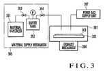
- An atomic layer growing apparatus to practice the atomic layer deposition having the above-described feature includes a film forming chamber 301 in which the vapor phase growth of a film is performed, a substrate table 302 having a heating mechanism accommodated in the film forming chamber 301, and an exhaust mechanism 304, as shown in Fig. 3 .
- the atomic layer growing apparatus also includes a material supply mechanism 305 including a source gas vaporizer 351 and buffer tank 352, and a purge gas supply unit 307.
- a substrate 303 to be processed is loaded onto the substrate table 302, and the film forming chamber 301 is sealed.
- the supply of a predetermined gas by the material supply mechanism 305, the evacuation of the chamber 301 by the exhaust mechanism 304, the purge of the surplus gas by supplying a purge gas by the purge gas supply unit 307, and the evacuation of the chamber 301 by the exhaust mechanism 304 are repeated, thereby forming a desired thin film.
- a material (organometallic material) used in the formation of an insulating film by the atomic layer growing apparatus is in the liquid phase at an atmospheric pressure of about 20°C.
- the material supply mechanism 305 vaporizes the material in the liquid phase by the source gas vaporizer 351, and supplies the vaporized material into the film forming chamber 301.
- the material supply mechanism 305 supplies a source gas into the film forming chamber 301 while a variation in pressure, for example, is suppressed by using the buffer tank 352.
- a supply valve 354 of the film forming chamber 301 is opened while a fill valve 353 of the buffer tank 352 is closed. This control can suppress a variation in pressure caused when the source gas from the source gas vaporizer 351 flows directly.
- the buffer tank 352 is filled with a source gas generated by the source gas vaporizer 351 while the supply valve 354 is closed and the fill valve 353 is open.
- the fill valve 353 is closed and the supply valve 354 is opened to supply the source gas by the buffer tank 352. Therefore, the source gas cannot be supplied into the film forming chamber 301 while the buffer tank 352 is filled with the source gas. Note that when the buffer tank 352 is filled with the source gas while the supply of the source gas is stopped in each cycle of the atomic layer deposition, it is possible to stably supply the source gas into the film forming chamber 301 at a given stage as needed.
- the conventional apparatus shown in Fig. 3 often cannot stably supply the source gas when each cycle of the atomic layer deposition is shortened.
- the present invention has been made to solve the above-described problem, and has as its object to make it possible to stably supply the source gas even when the source gas supply process in the atomic layer deposition is shortened.
- An atomic layer growing apparatus comprises at least a film forming chamber having an internal space which can be sealed, material vaporizing means for generating a source gas by vaporizing a material, a plurality of buffer tanks filled with a source gas generated by the material vaporizing means, fill valves which are respectively attached to the buffer tanks and control the filling of the source gas generated by the material vaporizing means, supply valves which respectively control the supply of a source gas from the buffer tanks, and control means for controlling opening/closing of the fill valves and the supply valves, wherein the control means performs control so that while the source gas is supplied into the film forming chamber by opening the supply valve of at least one of the buffer tanks, other buffer tanks the supply valves of which are not open are filled with a source gas by opening the fill valves of the other tanks.
- This apparatus can always supply the source gas into the film forming chamber while the source vaporizing means and the film forming chamber never communicate with each other.
- control means may control to supply the source gas into the film forming chamber by closing a supply valve of the buffer tank filled with a source gas by opening a fill valve of the buffer tank, and by opening a supply valve of a buffer tank filled with the source gas in excess of a prescribed lower limit.
- the above-described atomic layer growing apparatus may further comprise an injection control valve which controls injection of a source gas supplied from the buffer tanks into the film forming chamber, wherein the control means performs control so that while the source gas is supplied into the film forming chamber by opening the injection control valve and the supply valve of at least one of the buffer tanks, other buffer tanks the supply valves of which are not open are filled with a source gas by opening the fill valves of the other buffer tanks.
- the control means preferably controls to open the injection control valve while a supply valve of a buffer tank filled with a source gas by opening a fill valve of the buffer tank is closed, and a supply valve of a buffer tank filled with a source gas in excess of a prescribed lower limit is open.
- the pressure of the source gas which fills the buffer tank which supplies the source gas into the film forming chamber always exceeds the prescribed lower limit of its internal pressure while the source vaporizing means and the film forming chamber never communicate with each other.
- a plurality of buffer tanks are used so that, for example, the injection control valve is opened while the supply valve of a buffer tank filled with the source gas by opening its fill valve is closed, and the supply valve of a buffer tank filled with the source gas in excess of the prescribed lower limit of its internal pressure is open. That is, a plurality of buffer tanks are used so that while the source gas is supplied into the film forming chamber by opening the supply valve of at least one buffer tank, other buffer tanks the supply valves of which are not open are filled with the source gas by opening the fill valves of the other buffer tanks. This produces an excellent effect of more stably supplying the source gas into the film forming chamber even when the time for the source gas supply process in the atomic layer growth is shortened.
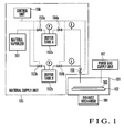
- Fig. 1 is a block diagram showing an example of the arrangement of an atomic layer growing apparatus according to the embodiment of the present invention.
- the atomic layer growing apparatus according to this embodiment shown in Fig. 1 includes a film forming chamber 101 in which the vapor phase growth of a film is performed, a substrate table 102 having a heating mechanism accommodated in the film forming chamber 101, and an exhaust mechanism 104.
- the film forming chamber 101 has an internal space which can be sealed, and accommodates the substrate table 102 in it.
- the atomic layer growing apparatus also includes a material supply unit 105 including a material vaporizer 151, two buffer banks, i.e., a buffer bank A 152a and buffer bank B 152b, a fill valve A 153a and supply valve A 154a of the buffer tank A 152a, a fill valve B 153b and supply valve B 154b of the buffer tank B 152b, an injection control valve 155, and a control unit 156 which controls the opening/closing of each valve.
- the atomic layer growing apparatus according to this embodiment also includes a purge gas supply unit 107 which supplies a purge gas formed from an inert gas such as argon or nitrogen into the film forming chamber 101.
- the material vaporizer 151 accommodates an organometallic material such as aminosilane, and vaporizes the accommodated organometallic material by heating to generate a source gas.
- the source gas generated in this way fills the buffer tank A 152a and buffer tank B 152b first. After that, the source gas which fills the buffer tank A 152a and that which fills the buffer tank B 152b are alternately supplied into the film forming chamber 101.
- the filling of the source gas into the buffer tanks, and the supply of the source gas from the buffer tanks are controlled by controlling the opening/closing of the fill valve A 153a, supply valve A 154a, fill valve B 153b, supply valve B 154b, and injection control valve 155 by the control unit 156.
- the control unit 156 keeps all of the fill valve A 153a, supply valve A 154a, fill valve B 153b, supply valve B 154b, and injection control valve 155 closed.
- the control unit 156 opens the supply valve A 154a and injection control valve 155 to supply the source gas from the buffer tank A 152a into the film forming chamber 101.
- the control unit 156 opens the fill valve B 153b to fill the buffer tank B 152b with the source gas.
- the control unit 156 closes the injection control valve 155.
- the control unit 156 opens the injection control valve 155.
- the control unit 156 closes the fill valve B 153b.
- the control unit 156 closes the supply valve A 154a and opens the fill valve A 153a and supply valve B 154b. With this operation, the source gas is supplied from the buffer tank B 152b into the film forming chamber 101.
- the control unit 156 closes the injection control valve 155.
- the control unit 156 opens the injection control valve 155.
- the control unit 156 closes the fill valve A 153a.
- the control unit 156 closes the injection control valve 155.
- the pressure of the source gas in the buffer tank B 152b becomes lower than its prescribed lower limit, so the control unit 156 closes the supply valve B 154b and opens the fill valve B 153b and supply valve A 154a.
- the control unit 156 opens the injection control valve 155. With this operation, the source gas is supplied from the buffer tank A 152a into the film forming chamber 101. When time t7 at which the source gas supply process ends and the purge process starts comes, the control unit 156 closes the injection control valve 155.
- the control unit 156 opens the injection control valve 155.
- the pressure of the source gas in the buffer tank A 152a becomes lower than its prescribed lower limit, so the control unit 156 closes the supply valve A 154a and opens the fill valve A 153a and supply valve B 154b. With this operation, the source gas is supplied from the buffer tank B 152b into the film forming chamber 101.
- the control unit 156 closes the injection control valve 155.
- the control unit 156 opens the injection control valve 155.
- the control unit 156 closes the fill valve A 153a.
- the control unit 156 closes the injection control valve 155. Also at time t11, the pressure of the source gas in the buffer tank B 152b becomes lower than its prescribed lower limit, so the control unit 156 closes the supply valve B 154b and opens the fill valve B 153b and supply valve A 154a.
- the control unit 156 opens the injection control valve 155. With this operation, the source gas is supplied from the buffer tank A 152a into the film forming chamber 101. Note that the pressure of the source gas described above need only be measured by a manometer P built in each buffer tank.
- a substrate 103 to be processed is loaded onto the substrate table 102, and the film forming chamber 101 is sealed. After that, while the substrate 103 is heated to a predetermined temperature by the heating mechanism of the substrate table 102, the above-described source gas supply process and the above-described purge process including the supply of the purge gas by the purge gas supply unit 107 and the evacuation of the chamber 101 by the exhaust mechanism 104 are repeated, thereby forming a desired thin film.
- the atomic layer growing apparatus uses two buffer tanks so that the source gas is supplied into the film forming chamber by opening the supply valve of one buffer tank, and the other buffer tank is filled with the source gas by opening the fill valve of the other buffer tank.
- this apparatus uses two buffer tanks so that the injection control valve is opened while the supply valve of a buffer tank filled with the source gas by opening its fill valve is closed, and the supply valve of a buffer tank filled with the source gas in excess of the prescribed lower limit of its internal pressure is open. The opening/closing of each valve is controlled by the control unit (control means).
- the material vaporizer 151 and film forming chamber 101 never communicate with each other in all the states. This suppresses a variation in pressure caused when the source gas from the material vaporizer 151 flows directly. Also, the pressure of the source gas which fills a buffer tank which supplies the source gas into the film forming chamber 101 can always exceed its prescribed lower limit. For this reason, even when the atomic layer deposition is performed at a cycle shorter than the time for which one buffer tank is filled with the source gas, the source gas is always supplied into the film forming chamber 101 in the source gas supply process, as shown in the timing chart of Fig. 2 . Also, the source gas is supplied into the film forming chamber 101 always at a stable pressure.
- the use of two buffer tanks allows suppression of wasting of the capacity of the material vaporizer 151 to generate a source gas.
- one buffer tank supplies the source gas
- the filling of the source gas is stopped while the source gas is supplied.
- the generation capacity of the material vaporizer 151 is wasted during the material supply process, which accounts for half the overall process.
- the time for which the filling of the source gas is stopped becomes shorter than the time for the material supply process, as indicated by "Filling State" shown in Fig. 2 . This suppresses wasting of the capacity of the material vaporizer 151 to generate a source gas.
- the supply valve of the other buffer tank is opened to supply the source gas up to the injection control valve 155.
- the injection control valve 155 is closed and the supply valve A 154a is opened at time t5.
- the present invention is not particularly limited to this, and the injection control valve 155 and supply valve A 154a may be opened at time t6. Note that a variation in pressure in the source gas supply can be further suppressed by performing the control shown in Fig. 2 by taking account of a delay of the source gas supply due to the presence of the capacity of the pipe from the supply valve to the injection control valve 155.
- the supply valve of this buffer tank is closed and its fill valve is opened, and the supply valve of the other buffer tank is opened at the same time.
- the pressure in the buffer tank A 152a becomes lower than its prescribed lower limit while the injection control valve 155 is open, so the supply valve A 154a is closed and the fill valve A 153a and supply valve B 154b are opened at the same time.
- the present invention is not particularly limited to this, and the two supply valves may be alternately opened/closed at the timing at which the injection control valve opens. For example, first, at time t0, the injection control valve 155 and supply valve A 154a are opened at the same time. Next, at time t2 at which the injection control valve 155 is opened, the supply valve A 154a is closed and the supply valve B 154b is opened at the same time. Lastly, at time t4 at which the injection control valve 155 is opened, the supply valve B 154b is closed and the supply valve A 154a is opened at the same time. Control is performed to repeat these operations. The fill valve A 153a and fill valve B 153b are controlled to open when the corresponding supply valve A 154a and supply valve B 154b are closed, and they are controlled to close when the pressures in the corresponding buffer tanks reach their specific upper limits.
- the source gas may be supplied into the film forming chamber by controlling the supply valve attached to each buffer tank without using the injection control valve.
- the control of each valve need only be performed as shown in the timing chart of Fig. 4 .
- This control will be explained.
- the injection control valve 155 is opened at all the stages (times).
- the buffer tank A 152a is filled with the source gas.
- the control unit 156 closes the fill valve A 153a, supply valve A 154a, fill valve B 153b, and supply valve B 154b.
- the control unit 156 opens the supply valve A 154a to supply the source gas from the buffer tank A 152a into the film forming chamber 101.
- the control unit 156 closes the supply valve A 154a to stop the source gas supply, and opens the fill valve A 153a to fill the buffer tank A 152a with the source gas.
- the control unit 156 opens the supply valve B 154b to supply the source gas from the buffer tank B 152b into the film forming chamber 101.
- the control unit 156 closes the fill valve A 153a.
- the control unit 156 closes the supply valve B 154b to stop the source gas supply, and opens the fill valve B 153b to fill the buffer tank B 152b with the source gas.
- the control unit 156 opens the supply valve A 154a to supply the source gas from the buffer tank A 152a into the film forming chamber 101.
- the control unit 156 closes the fill valve B 153b.
- the control unit 156 closes the supply valve A 154a to stop the source gas supply, and opens the fill valve A 153a to fill the buffer tank A 152a with the source gas.
- the control unit 156 opens the supply valve B 154b to supply the source gas from the buffer tank B 152b into the film forming chamber 101.
- the control unit 156 closes the fill valve A 153a.
- the control unit 156 closes the supply valve B 154b to stop the source gas supply, and opens the fill valve B 153b to fill the buffer tank B 152b with the source gas. After that, the above-described operation is repeated at times t8, t8', t9, t10, t10', t11, t12, t12',.... Note that the pressure of the source gas described above need only be measured by the manometer P built in each buffer bank.
- the material vaporizer 151 and film forming chamber 101 never communicate with each other. This suppresses a variation in pressure caused when the source gas from the material vaporizer 151 flows directly. Also even in this control, the period from time t1 to time t2' is taken for the filling, and the atomic layer deposition (source gas supply) is performed at a period (cycle) shorter than that period. Nevertheless, the source gas is always supplied into the film forming chamber 101 in the source gas supply process, as shown in the timing chart of Fig. 4 . Also, the source gas is supplied into the film forming chamber 101 always at a stable pressure.
- the present invention is not particularly limited to this.
- the flow rate of the source gas supplied from each supply valve may be measured by a flowmeter F, and the opening/closing of the supply valve of each buffer tank may be controlled on the basis of the measurement result of the flow rate, e.g., by confirming whether the flow rate measured exceeds a predetermined value.
- each buffer tank used need only include a fill valve which controls the filling of a source gas generated by a material vaporizer (material vaporizing means), and a supply valve which controls the supply of the source gas from the buffer tank.
- control need only be performed so that the injection control valve is opened while the supply valve of a buffer tank which fills the source gas by closing its fill valve is closed, and the supply valve of a buffer tank filled with the source gas in excess of the prescribed lower limit of its internal pressure is open.
- the atomic layer growing apparatus according to this embodiment shown in Fig. 1 is also applicable to atomic layer deposition which forms a metal oxide film using an oxidizing gas such as oxygen or ozone, in addition to that which uses a source gas containing an organometallic material.
- an oxidizing gas such as oxygen or ozone
- repeating organometallic source gas supply process ⁇ purge process ⁇ oxidizing gas supply process ⁇ purge process ⁇ ... makes it possible to form a metal oxide film. Even in this case, supplying, in turn, a source gas using a plurality of buffer tanks allows more stable source gas supply even when the time for the gas supply process is shortened.
- the present invention is preferably adopted in the crystal growth of a thin film made of a semiconductor or compound semiconductor, and the formation of, e.g., an oxide film.
Landscapes
- Chemical & Material Sciences (AREA)
- General Chemical & Material Sciences (AREA)
- Chemical Kinetics & Catalysis (AREA)
- Engineering & Computer Science (AREA)
- Materials Engineering (AREA)
- Mechanical Engineering (AREA)
- Metallurgy (AREA)
- Organic Chemistry (AREA)
- Chemical Vapour Deposition (AREA)
- Crystals, And After-Treatments Of Crystals (AREA)
Applications Claiming Priority (2)
| Application Number | Priority Date | Filing Date | Title |
|---|---|---|---|
| JP2006094466 | 2006-03-30 | ||
| PCT/JP2007/056622 WO2007114156A1 (fr) | 2006-03-30 | 2007-03-28 | appareil de croissance de couche atomique |
Publications (2)
| Publication Number | Publication Date |
|---|---|
| EP2006414A2 true EP2006414A2 (fr) | 2008-12-24 |
| EP2006414A9 EP2006414A9 (fr) | 2009-07-22 |
Family
ID=38563425
Family Applications (1)
| Application Number | Title | Priority Date | Filing Date |
|---|---|---|---|
| EP07740060A Withdrawn EP2006414A2 (fr) | 2006-03-30 | 2007-03-28 | Appareil de croissance de couche atomique |
Country Status (6)
| Country | Link |
|---|---|
| US (1) | US8202367B2 (fr) |
| EP (1) | EP2006414A2 (fr) |
| JP (1) | JP4866898B2 (fr) |
| KR (1) | KR101161020B1 (fr) |
| TW (1) | TW200741827A (fr) |
| WO (1) | WO2007114156A1 (fr) |
Cited By (7)
| Publication number | Priority date | Publication date | Assignee | Title |
|---|---|---|---|---|
| KR101246921B1 (ko) * | 2008-03-12 | 2013-03-25 | 미쯔이 죠센 가부시키가이샤 | 원료공급장치 |
| US8997686B2 (en) | 2010-09-29 | 2015-04-07 | Mks Instruments, Inc. | System for and method of fast pulse gas delivery |
| US9348339B2 (en) | 2010-09-29 | 2016-05-24 | Mks Instruments, Inc. | Method and apparatus for multiple-channel pulse gas delivery system |
| US10031531B2 (en) | 2011-02-25 | 2018-07-24 | Mks Instruments, Inc. | System for and method of multiple channel fast pulse gas delivery |
| US10126760B2 (en) | 2011-02-25 | 2018-11-13 | Mks Instruments, Inc. | System for and method of fast pulse gas delivery |
| US10353408B2 (en) | 2011-02-25 | 2019-07-16 | Mks Instruments, Inc. | System for and method of fast pulse gas delivery |
| WO2021097143A3 (fr) * | 2019-11-12 | 2021-08-19 | Forge Nano Inc. | Revêtements sur des particules de matériaux à haute énergie et leurs procédés de formation |
Families Citing this family (325)
| Publication number | Priority date | Publication date | Assignee | Title |
|---|---|---|---|---|
| EP2006414A2 (fr) * | 2006-03-30 | 2008-12-24 | Mitsui Engineering & Shipbuilding Co., Ltd. | Appareil de croissance de couche atomique |
| KR100851439B1 (ko) * | 2007-02-01 | 2008-08-11 | 주식회사 테라세미콘 | 소스가스 공급장치 |
| KR101028044B1 (ko) * | 2007-09-04 | 2011-04-08 | 주식회사 테라세미콘 | 소스가스 공급장치 |
| JP5355135B2 (ja) * | 2009-02-19 | 2013-11-27 | 中国電力株式会社 | 燃料電池発電設備 |
| JP5520552B2 (ja) | 2009-09-11 | 2014-06-11 | 株式会社日立国際電気 | 半導体装置の製造方法及び基板処理装置 |
| US20130023129A1 (en) | 2011-07-20 | 2013-01-24 | Asm America, Inc. | Pressure transmitter for a semiconductor processing environment |
| JP5824372B2 (ja) * | 2012-01-25 | 2015-11-25 | 東京エレクトロン株式会社 | 処理装置及びプロセス状態の確認方法 |
| US9238865B2 (en) | 2012-02-06 | 2016-01-19 | Asm Ip Holding B.V. | Multiple vapor sources for vapor deposition |
| JP5547762B2 (ja) * | 2012-03-12 | 2014-07-16 | 三井造船株式会社 | 薄膜形成装置 |
| US10714315B2 (en) | 2012-10-12 | 2020-07-14 | Asm Ip Holdings B.V. | Semiconductor reaction chamber showerhead |
| KR20140073198A (ko) | 2012-12-06 | 2014-06-16 | 삼성디스플레이 주식회사 | 유기물 기화 장치 및 그 제어방법 |
| US20160376700A1 (en) | 2013-02-01 | 2016-12-29 | Asm Ip Holding B.V. | System for treatment of deposition reactor |
| JP2015073020A (ja) * | 2013-10-03 | 2015-04-16 | 三井造船株式会社 | 原子層堆積装置および原子層堆積方法 |
| JP5859586B2 (ja) * | 2013-12-27 | 2016-02-10 | 株式会社日立国際電気 | 基板処理システム、半導体装置の製造方法および記録媒体 |
| US11015245B2 (en) | 2014-03-19 | 2021-05-25 | Asm Ip Holding B.V. | Gas-phase reactor and system having exhaust plenum and components thereof |
| US10858737B2 (en) | 2014-07-28 | 2020-12-08 | Asm Ip Holding B.V. | Showerhead assembly and components thereof |
| JP6359913B2 (ja) * | 2014-08-12 | 2018-07-18 | 東京エレクトロン株式会社 | 処理装置 |
| JP6415215B2 (ja) * | 2014-09-26 | 2018-10-31 | 株式会社Kokusai Electric | 基板処理装置、半導体装置の製造方法及びプログラム |
| US10941490B2 (en) | 2014-10-07 | 2021-03-09 | Asm Ip Holding B.V. | Multiple temperature range susceptor, assembly, reactor and system including the susceptor, and methods of using the same |
| JP2016134569A (ja) * | 2015-01-21 | 2016-07-25 | 株式会社東芝 | 半導体製造装置 |
| US10276355B2 (en) | 2015-03-12 | 2019-04-30 | Asm Ip Holding B.V. | Multi-zone reactor, system including the reactor, and method of using the same |
| US10458018B2 (en) | 2015-06-26 | 2019-10-29 | Asm Ip Holding B.V. | Structures including metal carbide material, devices including the structures, and methods of forming same |
| US10211308B2 (en) | 2015-10-21 | 2019-02-19 | Asm Ip Holding B.V. | NbMC layers |
| US11139308B2 (en) | 2015-12-29 | 2021-10-05 | Asm Ip Holding B.V. | Atomic layer deposition of III-V compounds to form V-NAND devices |
| US10529554B2 (en) | 2016-02-19 | 2020-01-07 | Asm Ip Holding B.V. | Method for forming silicon nitride film selectively on sidewalls or flat surfaces of trenches |
| US10343920B2 (en) | 2016-03-18 | 2019-07-09 | Asm Ip Holding B.V. | Aligned carbon nanotubes |
| US10367080B2 (en) | 2016-05-02 | 2019-07-30 | Asm Ip Holding B.V. | Method of forming a germanium oxynitride film |
| US11453943B2 (en) | 2016-05-25 | 2022-09-27 | Asm Ip Holding B.V. | Method for forming carbon-containing silicon/metal oxide or nitride film by ALD using silicon precursor and hydrocarbon precursor |
| US9859151B1 (en) | 2016-07-08 | 2018-01-02 | Asm Ip Holding B.V. | Selective film deposition method to form air gaps |
| US10612137B2 (en) | 2016-07-08 | 2020-04-07 | Asm Ip Holdings B.V. | Organic reactants for atomic layer deposition |
| US9812320B1 (en) | 2016-07-28 | 2017-11-07 | Asm Ip Holding B.V. | Method and apparatus for filling a gap |
| KR102532607B1 (ko) | 2016-07-28 | 2023-05-15 | 에이에스엠 아이피 홀딩 비.브이. | 기판 가공 장치 및 그 동작 방법 |
| US9887082B1 (en) | 2016-07-28 | 2018-02-06 | Asm Ip Holding B.V. | Method and apparatus for filling a gap |
| US11532757B2 (en) | 2016-10-27 | 2022-12-20 | Asm Ip Holding B.V. | Deposition of charge trapping layers |
| US10714350B2 (en) | 2016-11-01 | 2020-07-14 | ASM IP Holdings, B.V. | Methods for forming a transition metal niobium nitride film on a substrate by atomic layer deposition and related semiconductor device structures |
| KR102546317B1 (ko) | 2016-11-15 | 2023-06-21 | 에이에스엠 아이피 홀딩 비.브이. | 기체 공급 유닛 및 이를 포함하는 기판 처리 장치 |
| JP7062658B2 (ja) | 2016-12-09 | 2022-05-06 | エーエスエム アイピー ホールディング ビー.ブイ. | 熱原子層エッチングプロセス |
| KR102762543B1 (ko) | 2016-12-14 | 2025-02-05 | 에이에스엠 아이피 홀딩 비.브이. | 기판 처리 장치 |
| US11447861B2 (en) | 2016-12-15 | 2022-09-20 | Asm Ip Holding B.V. | Sequential infiltration synthesis apparatus and a method of forming a patterned structure |
| US11581186B2 (en) | 2016-12-15 | 2023-02-14 | Asm Ip Holding B.V. | Sequential infiltration synthesis apparatus |
| KR102700194B1 (ko) | 2016-12-19 | 2024-08-28 | 에이에스엠 아이피 홀딩 비.브이. | 기판 처리 장치 |
| US10283319B2 (en) | 2016-12-22 | 2019-05-07 | Asm Ip Holding B.V. | Atomic layer etching processes |
| US10269558B2 (en) | 2016-12-22 | 2019-04-23 | Asm Ip Holding B.V. | Method of forming a structure on a substrate |
| US11390950B2 (en) | 2017-01-10 | 2022-07-19 | Asm Ip Holding B.V. | Reactor system and method to reduce residue buildup during a film deposition process |
| US10468261B2 (en) | 2017-02-15 | 2019-11-05 | Asm Ip Holding B.V. | Methods for forming a metallic film on a substrate by cyclical deposition and related semiconductor device structures |
| US10529563B2 (en) | 2017-03-29 | 2020-01-07 | Asm Ip Holdings B.V. | Method for forming doped metal oxide films on a substrate by cyclical deposition and related semiconductor device structures |
| US10770286B2 (en) | 2017-05-08 | 2020-09-08 | Asm Ip Holdings B.V. | Methods for selectively forming a silicon nitride film on a substrate and related semiconductor device structures |
| JP7105765B2 (ja) * | 2017-05-11 | 2022-07-25 | 株式会社堀場エステック | 液体材料気化供給装置及び制御プログラム |
| US12040200B2 (en) | 2017-06-20 | 2024-07-16 | Asm Ip Holding B.V. | Semiconductor processing apparatus and methods for calibrating a semiconductor processing apparatus |
| US11306395B2 (en) | 2017-06-28 | 2022-04-19 | Asm Ip Holding B.V. | Methods for depositing a transition metal nitride film on a substrate by atomic layer deposition and related deposition apparatus |
| JP7107648B2 (ja) | 2017-07-11 | 2022-07-27 | 株式会社堀場エステック | 流体制御装置、流体制御システム、流体制御方法、及び、流体制御装置用プログラム |
| TWI794238B (zh) | 2017-07-13 | 2023-03-01 | 荷蘭商Asm智慧財產控股公司 | 於單一加工腔室中自半導體膜移除氧化物及碳之裝置及方法 |
| KR20190009245A (ko) | 2017-07-18 | 2019-01-28 | 에이에스엠 아이피 홀딩 비.브이. | 반도체 소자 구조물 형성 방법 및 관련된 반도체 소자 구조물 |
| US11018002B2 (en) | 2017-07-19 | 2021-05-25 | Asm Ip Holding B.V. | Method for selectively depositing a Group IV semiconductor and related semiconductor device structures |
| US10541333B2 (en) | 2017-07-19 | 2020-01-21 | Asm Ip Holding B.V. | Method for depositing a group IV semiconductor and related semiconductor device structures |
| US11374112B2 (en) | 2017-07-19 | 2022-06-28 | Asm Ip Holding B.V. | Method for depositing a group IV semiconductor and related semiconductor device structures |
| US10590535B2 (en) | 2017-07-26 | 2020-03-17 | Asm Ip Holdings B.V. | Chemical treatment, deposition and/or infiltration apparatus and method for using the same |
| TWI815813B (zh) | 2017-08-04 | 2023-09-21 | 荷蘭商Asm智慧財產控股公司 | 用於分配反應腔內氣體的噴頭總成 |
| US10770336B2 (en) | 2017-08-08 | 2020-09-08 | Asm Ip Holding B.V. | Substrate lift mechanism and reactor including same |
| US10692741B2 (en) | 2017-08-08 | 2020-06-23 | Asm Ip Holdings B.V. | Radiation shield |
| US11769682B2 (en) | 2017-08-09 | 2023-09-26 | Asm Ip Holding B.V. | Storage apparatus for storing cassettes for substrates and processing apparatus equipped therewith |
| US11139191B2 (en) | 2017-08-09 | 2021-10-05 | Asm Ip Holding B.V. | Storage apparatus for storing cassettes for substrates and processing apparatus equipped therewith |
| US11830730B2 (en) | 2017-08-29 | 2023-11-28 | Asm Ip Holding B.V. | Layer forming method and apparatus |
| KR102491945B1 (ko) | 2017-08-30 | 2023-01-26 | 에이에스엠 아이피 홀딩 비.브이. | 기판 처리 장치 |
| US11056344B2 (en) | 2017-08-30 | 2021-07-06 | Asm Ip Holding B.V. | Layer forming method |
| US11295980B2 (en) | 2017-08-30 | 2022-04-05 | Asm Ip Holding B.V. | Methods for depositing a molybdenum metal film over a dielectric surface of a substrate by a cyclical deposition process and related semiconductor device structures |
| US10658205B2 (en) | 2017-09-28 | 2020-05-19 | Asm Ip Holdings B.V. | Chemical dispensing apparatus and methods for dispensing a chemical to a reaction chamber |
| US10403504B2 (en) | 2017-10-05 | 2019-09-03 | Asm Ip Holding B.V. | Method for selectively depositing a metallic film on a substrate |
| US10923344B2 (en) | 2017-10-30 | 2021-02-16 | Asm Ip Holding B.V. | Methods for forming a semiconductor structure and related semiconductor structures |
| US11022879B2 (en) | 2017-11-24 | 2021-06-01 | Asm Ip Holding B.V. | Method of forming an enhanced unexposed photoresist layer |
| TWI791689B (zh) | 2017-11-27 | 2023-02-11 | 荷蘭商Asm智慧財產控股私人有限公司 | 包括潔淨迷你環境之裝置 |
| WO2019103613A1 (fr) | 2017-11-27 | 2019-05-31 | Asm Ip Holding B.V. | Dispositif de stockage pour stocker des cassettes de tranches destiné à être utilisé avec un four discontinu |
| US10872771B2 (en) | 2018-01-16 | 2020-12-22 | Asm Ip Holding B. V. | Method for depositing a material film on a substrate within a reaction chamber by a cyclical deposition process and related device structures |
| US11482412B2 (en) | 2018-01-19 | 2022-10-25 | Asm Ip Holding B.V. | Method for depositing a gap-fill layer by plasma-assisted deposition |
| TWI799494B (zh) | 2018-01-19 | 2023-04-21 | 荷蘭商Asm 智慧財產控股公司 | 沈積方法 |
| US11081345B2 (en) | 2018-02-06 | 2021-08-03 | Asm Ip Holding B.V. | Method of post-deposition treatment for silicon oxide film |
| US10896820B2 (en) | 2018-02-14 | 2021-01-19 | Asm Ip Holding B.V. | Method for depositing a ruthenium-containing film on a substrate by a cyclical deposition process |
| WO2019158960A1 (fr) | 2018-02-14 | 2019-08-22 | Asm Ip Holding B.V. | Procédé de dépôt d'un film contenant du ruthénium sur un substrat par un processus de dépôt cyclique |
| US10731249B2 (en) | 2018-02-15 | 2020-08-04 | Asm Ip Holding B.V. | Method of forming a transition metal containing film on a substrate by a cyclical deposition process, a method for supplying a transition metal halide compound to a reaction chamber, and related vapor deposition apparatus |
| KR102636427B1 (ko) | 2018-02-20 | 2024-02-13 | 에이에스엠 아이피 홀딩 비.브이. | 기판 처리 방법 및 장치 |
| US10975470B2 (en) | 2018-02-23 | 2021-04-13 | Asm Ip Holding B.V. | Apparatus for detecting or monitoring for a chemical precursor in a high temperature environment |
| US11473195B2 (en) | 2018-03-01 | 2022-10-18 | Asm Ip Holding B.V. | Semiconductor processing apparatus and a method for processing a substrate |
| US11629406B2 (en) | 2018-03-09 | 2023-04-18 | Asm Ip Holding B.V. | Semiconductor processing apparatus comprising one or more pyrometers for measuring a temperature of a substrate during transfer of the substrate |
| US11114283B2 (en) | 2018-03-16 | 2021-09-07 | Asm Ip Holding B.V. | Reactor, system including the reactor, and methods of manufacturing and using same |
| CN111837223B (zh) * | 2018-03-22 | 2025-02-25 | 株式会社国际电气 | 基板处理装置、半导体装置的制造方法和记录介质 |
| KR102646467B1 (ko) | 2018-03-27 | 2024-03-11 | 에이에스엠 아이피 홀딩 비.브이. | 기판 상에 전극을 형성하는 방법 및 전극을 포함하는 반도체 소자 구조 |
| US11088002B2 (en) | 2018-03-29 | 2021-08-10 | Asm Ip Holding B.V. | Substrate rack and a substrate processing system and method |
| US11230766B2 (en) | 2018-03-29 | 2022-01-25 | Asm Ip Holding B.V. | Substrate processing apparatus and method |
| KR102504958B1 (ko) | 2018-04-02 | 2023-03-03 | 삼성전자주식회사 | 박막 증착 방법 및 박막 증착 장치 |
| KR102600229B1 (ko) | 2018-04-09 | 2023-11-10 | 에이에스엠 아이피 홀딩 비.브이. | 기판 지지 장치, 이를 포함하는 기판 처리 장치 및 기판 처리 방법 |
| TWI843623B (zh) | 2018-05-08 | 2024-05-21 | 荷蘭商Asm Ip私人控股有限公司 | 藉由循環沉積製程於基板上沉積氧化物膜之方法及相關裝置結構 |
| US12025484B2 (en) | 2018-05-08 | 2024-07-02 | Asm Ip Holding B.V. | Thin film forming method |
| US12272527B2 (en) | 2018-05-09 | 2025-04-08 | Asm Ip Holding B.V. | Apparatus for use with hydrogen radicals and method of using same |
| KR102596988B1 (ko) | 2018-05-28 | 2023-10-31 | 에이에스엠 아이피 홀딩 비.브이. | 기판 처리 방법 및 그에 의해 제조된 장치 |
| US11718913B2 (en) | 2018-06-04 | 2023-08-08 | Asm Ip Holding B.V. | Gas distribution system and reactor system including same |
| TWI840362B (zh) | 2018-06-04 | 2024-05-01 | 荷蘭商Asm Ip私人控股有限公司 | 水氣降低的晶圓處置腔室 |
| US11286562B2 (en) | 2018-06-08 | 2022-03-29 | Asm Ip Holding B.V. | Gas-phase chemical reactor and method of using same |
| KR102568797B1 (ko) | 2018-06-21 | 2023-08-21 | 에이에스엠 아이피 홀딩 비.브이. | 기판 처리 시스템 |
| US10797133B2 (en) | 2018-06-21 | 2020-10-06 | Asm Ip Holding B.V. | Method for depositing a phosphorus doped silicon arsenide film and related semiconductor device structures |
| WO2020003000A1 (fr) | 2018-06-27 | 2020-01-02 | Asm Ip Holding B.V. | Procédés de dépôt cyclique pour former un matériau contenant du métal et films et structures comprenant le matériau contenant du métal |
| KR20250134000A (ko) | 2018-06-27 | 2025-09-09 | 에이에스엠 아이피 홀딩 비.브이. | 금속 함유 재료를 형성하기 위한 주기적 증착 방법 및 금속 함유 재료를 포함하는 필름 및 구조체 |
| US10612136B2 (en) | 2018-06-29 | 2020-04-07 | ASM IP Holding, B.V. | Temperature-controlled flange and reactor system including same |
| US10388513B1 (en) | 2018-07-03 | 2019-08-20 | Asm Ip Holding B.V. | Method for depositing silicon-free carbon-containing film as gap-fill layer by pulse plasma-assisted deposition |
| US10755922B2 (en) | 2018-07-03 | 2020-08-25 | Asm Ip Holding B.V. | Method for depositing silicon-free carbon-containing film as gap-fill layer by pulse plasma-assisted deposition |
| US11053591B2 (en) | 2018-08-06 | 2021-07-06 | Asm Ip Holding B.V. | Multi-port gas injection system and reactor system including same |
| US11430674B2 (en) | 2018-08-22 | 2022-08-30 | Asm Ip Holding B.V. | Sensor array, apparatus for dispensing a vapor phase reactant to a reaction chamber and related methods |
| KR102707956B1 (ko) | 2018-09-11 | 2024-09-19 | 에이에스엠 아이피 홀딩 비.브이. | 박막 증착 방법 |
| US11024523B2 (en) | 2018-09-11 | 2021-06-01 | Asm Ip Holding B.V. | Substrate processing apparatus and method |
| US11049751B2 (en) | 2018-09-14 | 2021-06-29 | Asm Ip Holding B.V. | Cassette supply system to store and handle cassettes and processing apparatus equipped therewith |
| CN110970344B (zh) | 2018-10-01 | 2024-10-25 | Asmip控股有限公司 | 衬底保持设备、包含所述设备的系统及其使用方法 |
| US11232963B2 (en) | 2018-10-03 | 2022-01-25 | Asm Ip Holding B.V. | Substrate processing apparatus and method |
| KR102592699B1 (ko) | 2018-10-08 | 2023-10-23 | 에이에스엠 아이피 홀딩 비.브이. | 기판 지지 유닛 및 이를 포함하는 박막 증착 장치와 기판 처리 장치 |
| KR102546322B1 (ko) | 2018-10-19 | 2023-06-21 | 에이에스엠 아이피 홀딩 비.브이. | 기판 처리 장치 및 기판 처리 방법 |
| KR102605121B1 (ko) | 2018-10-19 | 2023-11-23 | 에이에스엠 아이피 홀딩 비.브이. | 기판 처리 장치 및 기판 처리 방법 |
| USD948463S1 (en) | 2018-10-24 | 2022-04-12 | Asm Ip Holding B.V. | Susceptor for semiconductor substrate supporting apparatus |
| US12378665B2 (en) | 2018-10-26 | 2025-08-05 | Asm Ip Holding B.V. | High temperature coatings for a preclean and etch apparatus and related methods |
| US11087997B2 (en) | 2018-10-31 | 2021-08-10 | Asm Ip Holding B.V. | Substrate processing apparatus for processing substrates |
| KR102748291B1 (ko) | 2018-11-02 | 2024-12-31 | 에이에스엠 아이피 홀딩 비.브이. | 기판 지지 유닛 및 이를 포함하는 기판 처리 장치 |
| US11572620B2 (en) | 2018-11-06 | 2023-02-07 | Asm Ip Holding B.V. | Methods for selectively depositing an amorphous silicon film on a substrate |
| US11031242B2 (en) | 2018-11-07 | 2021-06-08 | Asm Ip Holding B.V. | Methods for depositing a boron doped silicon germanium film |
| US10847366B2 (en) | 2018-11-16 | 2020-11-24 | Asm Ip Holding B.V. | Methods for depositing a transition metal chalcogenide film on a substrate by a cyclical deposition process |
| US10818758B2 (en) | 2018-11-16 | 2020-10-27 | Asm Ip Holding B.V. | Methods for forming a metal silicate film on a substrate in a reaction chamber and related semiconductor device structures |
| JP7259281B2 (ja) * | 2018-11-21 | 2023-04-18 | 東京エレクトロン株式会社 | 基板処理装置、基板処理システム及び基板処理方法 |
| US12040199B2 (en) | 2018-11-28 | 2024-07-16 | Asm Ip Holding B.V. | Substrate processing apparatus for processing substrates |
| US11217444B2 (en) | 2018-11-30 | 2022-01-04 | Asm Ip Holding B.V. | Method for forming an ultraviolet radiation responsive metal oxide-containing film |
| KR102636428B1 (ko) | 2018-12-04 | 2024-02-13 | 에이에스엠 아이피 홀딩 비.브이. | 기판 처리 장치를 세정하는 방법 |
| US11158513B2 (en) | 2018-12-13 | 2021-10-26 | Asm Ip Holding B.V. | Methods for forming a rhenium-containing film on a substrate by a cyclical deposition process and related semiconductor device structures |
| JP7504584B2 (ja) | 2018-12-14 | 2024-06-24 | エーエスエム・アイピー・ホールディング・ベー・フェー | 窒化ガリウムの選択的堆積を用いてデバイス構造体を形成する方法及びそのためのシステム |
| JP7246184B2 (ja) * | 2018-12-27 | 2023-03-27 | 東京エレクトロン株式会社 | RuSi膜の形成方法 |
| TWI866480B (zh) | 2019-01-17 | 2024-12-11 | 荷蘭商Asm Ip 私人控股有限公司 | 藉由循環沈積製程於基板上形成含過渡金屬膜之方法 |
| KR102727227B1 (ko) | 2019-01-22 | 2024-11-07 | 에이에스엠 아이피 홀딩 비.브이. | 기판 처리 장치 |
| CN111524788B (zh) | 2019-02-01 | 2023-11-24 | Asm Ip私人控股有限公司 | 氧化硅的拓扑选择性膜形成的方法 |
| JP6902060B2 (ja) * | 2019-02-13 | 2021-07-14 | 株式会社Kokusai Electric | 基板処理装置、半導体装置の製造方法、およびプログラム |
| TWI838458B (zh) | 2019-02-20 | 2024-04-11 | 荷蘭商Asm Ip私人控股有限公司 | 用於3d nand應用中之插塞填充沉積之設備及方法 |
| KR102638425B1 (ko) | 2019-02-20 | 2024-02-21 | 에이에스엠 아이피 홀딩 비.브이. | 기판 표면 내에 형성된 오목부를 충진하기 위한 방법 및 장치 |
| TWI845607B (zh) | 2019-02-20 | 2024-06-21 | 荷蘭商Asm Ip私人控股有限公司 | 用來填充形成於基材表面內之凹部的循環沉積方法及設備 |
| KR102626263B1 (ko) | 2019-02-20 | 2024-01-16 | 에이에스엠 아이피 홀딩 비.브이. | 처리 단계를 포함하는 주기적 증착 방법 및 이를 위한 장치 |
| TWI842826B (zh) | 2019-02-22 | 2024-05-21 | 荷蘭商Asm Ip私人控股有限公司 | 基材處理設備及處理基材之方法 |
| KR102782593B1 (ko) | 2019-03-08 | 2025-03-14 | 에이에스엠 아이피 홀딩 비.브이. | SiOC 층을 포함한 구조체 및 이의 형성 방법 |
| US11742198B2 (en) | 2019-03-08 | 2023-08-29 | Asm Ip Holding B.V. | Structure including SiOCN layer and method of forming same |
| KR102858005B1 (ko) | 2019-03-08 | 2025-09-09 | 에이에스엠 아이피 홀딩 비.브이. | 실리콘 질화물 층을 선택적으로 증착하는 방법, 및 선택적으로 증착된 실리콘 질화물 층을 포함하는 구조체 |
| JP2020167398A (ja) | 2019-03-28 | 2020-10-08 | エーエスエム・アイピー・ホールディング・ベー・フェー | ドアオープナーおよびドアオープナーが提供される基材処理装置 |
| KR102809999B1 (ko) | 2019-04-01 | 2025-05-19 | 에이에스엠 아이피 홀딩 비.브이. | 반도체 소자를 제조하는 방법 |
| KR102897355B1 (ko) | 2019-04-19 | 2025-12-08 | 에이에스엠 아이피 홀딩 비.브이. | 층 형성 방법 및 장치 |
| KR20200125453A (ko) | 2019-04-24 | 2020-11-04 | 에이에스엠 아이피 홀딩 비.브이. | 기상 반응기 시스템 및 이를 사용하는 방법 |
| KR102929471B1 (ko) | 2019-05-07 | 2026-02-20 | 에이에스엠 아이피 홀딩 비.브이. | 딥 튜브가 있는 화학물질 공급원 용기 |
| KR102869364B1 (ko) | 2019-05-07 | 2025-10-10 | 에이에스엠 아이피 홀딩 비.브이. | 비정질 탄소 중합체 막을 개질하는 방법 |
| KR102929472B1 (ko) | 2019-05-10 | 2026-02-20 | 에이에스엠 아이피 홀딩 비.브이. | 표면 상에 재료를 증착하는 방법 및 본 방법에 따라 형성된 구조 |
| JP7598201B2 (ja) | 2019-05-16 | 2024-12-11 | エーエスエム・アイピー・ホールディング・ベー・フェー | ウェハボートハンドリング装置、縦型バッチ炉および方法 |
| JP7612342B2 (ja) | 2019-05-16 | 2025-01-14 | エーエスエム・アイピー・ホールディング・ベー・フェー | ウェハボートハンドリング装置、縦型バッチ炉および方法 |
| USD975665S1 (en) | 2019-05-17 | 2023-01-17 | Asm Ip Holding B.V. | Susceptor shaft |
| USD947913S1 (en) | 2019-05-17 | 2022-04-05 | Asm Ip Holding B.V. | Susceptor shaft |
| USD935572S1 (en) | 2019-05-24 | 2021-11-09 | Asm Ip Holding B.V. | Gas channel plate |
| USD922229S1 (en) | 2019-06-05 | 2021-06-15 | Asm Ip Holding B.V. | Device for controlling a temperature of a gas supply unit |
| KR20200141003A (ko) | 2019-06-06 | 2020-12-17 | 에이에스엠 아이피 홀딩 비.브이. | 가스 감지기를 포함하는 기상 반응기 시스템 |
| KR102918757B1 (ko) | 2019-06-10 | 2026-01-28 | 에이에스엠 아이피 홀딩 비.브이. | 석영 에피택셜 챔버를 세정하는 방법 |
| KR20200143254A (ko) | 2019-06-11 | 2020-12-23 | 에이에스엠 아이피 홀딩 비.브이. | 개질 가스를 사용하여 전자 구조를 형성하는 방법, 상기 방법을 수행하기 위한 시스템, 및 상기 방법을 사용하여 형성되는 구조 |
| USD944946S1 (en) | 2019-06-14 | 2022-03-01 | Asm Ip Holding B.V. | Shower plate |
| USD931978S1 (en) | 2019-06-27 | 2021-09-28 | Asm Ip Holding B.V. | Showerhead vacuum transport |
| KR102911421B1 (ko) | 2019-07-03 | 2026-01-12 | 에이에스엠 아이피 홀딩 비.브이. | 기판 처리 장치용 온도 제어 조립체 및 이를 사용하는 방법 |
| US11788190B2 (en) * | 2019-07-05 | 2023-10-17 | Asm Ip Holding B.V. | Liquid vaporizer |
| JP7499079B2 (ja) | 2019-07-09 | 2024-06-13 | エーエスエム・アイピー・ホールディング・ベー・フェー | 同軸導波管を用いたプラズマ装置、基板処理方法 |
| CN112216646B (zh) | 2019-07-10 | 2026-02-10 | Asmip私人控股有限公司 | 基板支撑组件及包括其的基板处理装置 |
| JP7296806B2 (ja) | 2019-07-16 | 2023-06-23 | 東京エレクトロン株式会社 | RuSi膜の形成方法及び基板処理システム |
| KR102895115B1 (ko) | 2019-07-16 | 2025-12-03 | 에이에스엠 아이피 홀딩 비.브이. | 기판 처리 장치 |
| KR102955799B1 (ko) | 2019-07-17 | 2026-04-21 | 에이에스엠 아이피 홀딩 비.브이. | 라디칼 보조 점화 플라즈마 시스템 및 방법 |
| KR102860110B1 (ko) | 2019-07-17 | 2025-09-16 | 에이에스엠 아이피 홀딩 비.브이. | 실리콘 게르마늄 구조를 형성하는 방법 |
| US11643724B2 (en) | 2019-07-18 | 2023-05-09 | Asm Ip Holding B.V. | Method of forming structures using a neutral beam |
| JP7737789B2 (ja) | 2019-07-18 | 2025-09-11 | エーエスエム・アイピー・ホールディング・ベー・フェー | 半導体処理システム用シャワーヘッドデバイス |
| JP7548740B2 (ja) * | 2019-07-18 | 2024-09-10 | エーエスエム・アイピー・ホールディング・ベー・フェー | 中間チャンバーを備える半導体気相エッチング装置 |
| KR102903090B1 (ko) | 2019-07-19 | 2025-12-19 | 에이에스엠 아이피 홀딩 비.브이. | 토폴로지-제어된 비정질 탄소 중합체 막을 형성하는 방법 |
| TWI839544B (zh) | 2019-07-19 | 2024-04-21 | 荷蘭商Asm Ip私人控股有限公司 | 形成形貌受控的非晶碳聚合物膜之方法 |
| TWI851767B (zh) | 2019-07-29 | 2024-08-11 | 荷蘭商Asm Ip私人控股有限公司 | 用於利用n型摻雜物及/或替代摻雜物選擇性沉積以達成高摻雜物併入之方法 |
| KR102971074B1 (ko) | 2019-07-30 | 2026-05-29 | 에이에스엠 아이피 홀딩 비.브이. | 기판 처리 장치 및 방법 |
| CN112309899B (zh) | 2019-07-30 | 2025-11-14 | Asmip私人控股有限公司 | 基板处理设备 |
| CN112309900B (zh) | 2019-07-30 | 2025-11-04 | Asmip私人控股有限公司 | 基板处理设备 |
| US12622218B2 (en) | 2019-07-31 | 2026-05-05 | Asm Ip Holding B.V. | Cassette lid opening device |
| US11587815B2 (en) | 2019-07-31 | 2023-02-21 | Asm Ip Holding B.V. | Vertical batch furnace assembly |
| US11587814B2 (en) | 2019-07-31 | 2023-02-21 | Asm Ip Holding B.V. | Vertical batch furnace assembly |
| US11227782B2 (en) | 2019-07-31 | 2022-01-18 | Asm Ip Holding B.V. | Vertical batch furnace assembly |
| CN112323048B (zh) | 2019-08-05 | 2024-02-09 | Asm Ip私人控股有限公司 | 用于化学源容器的液位传感器 |
| CN112342526A (zh) | 2019-08-09 | 2021-02-09 | Asm Ip私人控股有限公司 | 包括冷却装置的加热器组件及其使用方法 |
| USD965524S1 (en) | 2019-08-19 | 2022-10-04 | Asm Ip Holding B.V. | Susceptor support |
| USD965044S1 (en) | 2019-08-19 | 2022-09-27 | Asm Ip Holding B.V. | Susceptor shaft |
| JP7810514B2 (ja) | 2019-08-21 | 2026-02-03 | エーエスエム・アイピー・ホールディング・ベー・フェー | 成膜原料混合ガス生成装置及び成膜装置 |
| USD949319S1 (en) | 2019-08-22 | 2022-04-19 | Asm Ip Holding B.V. | Exhaust duct |
| USD979506S1 (en) | 2019-08-22 | 2023-02-28 | Asm Ip Holding B.V. | Insulator |
| KR102983146B1 (ko) | 2019-08-22 | 2026-06-26 | 에이에스엠 아이피 홀딩 비.브이. | 홀을 구비한 구조체를 형성하기 위한 방법 |
| USD930782S1 (en) | 2019-08-22 | 2021-09-14 | Asm Ip Holding B.V. | Gas distributor |
| USD940837S1 (en) | 2019-08-22 | 2022-01-11 | Asm Ip Holding B.V. | Electrode |
| US11286558B2 (en) | 2019-08-23 | 2022-03-29 | Asm Ip Holding B.V. | Methods for depositing a molybdenum nitride film on a surface of a substrate by a cyclical deposition process and related semiconductor device structures including a molybdenum nitride film |
| KR102928101B1 (ko) | 2019-08-23 | 2026-02-13 | 에이에스엠 아이피 홀딩 비.브이. | 비스(디에틸아미노)실란을 사용하여 peald에 의해 개선된 품질을 갖는 실리콘 산화물 막을 증착하기 위한 방법 |
| CN112442674A (zh) | 2019-09-03 | 2021-03-05 | Asm Ip私人控股有限公司 | 用于沉积硫族化物膜的方法和设备以及包括膜的结构 |
| KR102806450B1 (ko) | 2019-09-04 | 2025-05-12 | 에이에스엠 아이피 홀딩 비.브이. | 희생 캡핑 층을 이용한 선택적 증착 방법 |
| KR102733104B1 (ko) | 2019-09-05 | 2024-11-22 | 에이에스엠 아이피 홀딩 비.브이. | 기판 처리 장치 |
| US12469693B2 (en) | 2019-09-17 | 2025-11-11 | Asm Ip Holding B.V. | Method of forming a carbon-containing layer and structure including the layer |
| US11946136B2 (en) | 2019-09-20 | 2024-04-02 | Asm Ip Holding B.V. | Semiconductor processing device |
| US11562901B2 (en) | 2019-09-25 | 2023-01-24 | Asm Ip Holding B.V. | Substrate processing method |
| CN112593212B (zh) | 2019-10-02 | 2023-12-22 | Asm Ip私人控股有限公司 | 通过循环等离子体增强沉积工艺形成拓扑选择性氧化硅膜的方法 |
| KR102948143B1 (ko) | 2019-10-08 | 2026-04-07 | 에이에스엠 아이피 홀딩 비.브이. | 활성 종을 이용하기 위한 가스 분배 어셈블리를 포함한 반응기 시스템 및 이를 사용하는 방법 |
| TWI925822B (zh) | 2019-10-08 | 2026-05-21 | 荷蘭商Asm Ip私人控股有限公司 | 氣體注入系統、及將材料沉積於反應室內之基板表面上的方法 |
| TWI846953B (zh) | 2019-10-08 | 2024-07-01 | 荷蘭商Asm Ip私人控股有限公司 | 基板處理裝置 |
| KR102879443B1 (ko) | 2019-10-10 | 2025-11-03 | 에이에스엠 아이피 홀딩 비.브이. | 포토레지스트 하부층을 형성하기 위한 방법 및 이를 포함한 구조체 |
| US12009241B2 (en) | 2019-10-14 | 2024-06-11 | Asm Ip Holding B.V. | Vertical batch furnace assembly with detector to detect cassette |
| TWI834919B (zh) | 2019-10-16 | 2024-03-11 | 荷蘭商Asm Ip私人控股有限公司 | 氧化矽之拓撲選擇性膜形成之方法 |
| US11637014B2 (en) | 2019-10-17 | 2023-04-25 | Asm Ip Holding B.V. | Methods for selective deposition of doped semiconductor material |
| KR102845724B1 (ko) | 2019-10-21 | 2025-08-13 | 에이에스엠 아이피 홀딩 비.브이. | 막을 선택적으로 에칭하기 위한 장치 및 방법 |
| KR102960940B1 (ko) | 2019-10-25 | 2026-05-04 | 에이에스엠 아이피 홀딩 비.브이. | 기판 표면 상의 갭 피처를 충진하는 방법 및 이와 관련된 반도체 소자 구조 |
| US11646205B2 (en) | 2019-10-29 | 2023-05-09 | Asm Ip Holding B.V. | Methods of selectively forming n-type doped material on a surface, systems for selectively forming n-type doped material, and structures formed using same |
| KR102890638B1 (ko) | 2019-11-05 | 2025-11-25 | 에이에스엠 아이피 홀딩 비.브이. | 도핑된 반도체 층을 갖는 구조체 및 이를 형성하기 위한 방법 및 시스템 |
| US11501968B2 (en) | 2019-11-15 | 2022-11-15 | Asm Ip Holding B.V. | Method for providing a semiconductor device with silicon filled gaps |
| KR102861314B1 (ko) | 2019-11-20 | 2025-09-17 | 에이에스엠 아이피 홀딩 비.브이. | 기판의 표면 상에 탄소 함유 물질을 증착하는 방법, 상기 방법을 사용하여 형성된 구조물, 및 상기 구조물을 형성하기 위한 시스템 |
| CN112951697B (zh) | 2019-11-26 | 2025-07-29 | Asmip私人控股有限公司 | 基板处理设备 |
| KR20210065848A (ko) | 2019-11-26 | 2021-06-04 | 에이에스엠 아이피 홀딩 비.브이. | 제1 유전체 표면과 제2 금속성 표면을 포함한 기판 상에 타겟 막을 선택적으로 형성하기 위한 방법 |
| CN120998766A (zh) | 2019-11-29 | 2025-11-21 | Asm Ip私人控股有限公司 | 基板处理设备 |
| CN120432376A (zh) | 2019-11-29 | 2025-08-05 | Asm Ip私人控股有限公司 | 基板处理设备 |
| JP7527928B2 (ja) | 2019-12-02 | 2024-08-05 | エーエスエム・アイピー・ホールディング・ベー・フェー | 基板処理装置、基板処理方法 |
| KR20210070898A (ko) | 2019-12-04 | 2021-06-15 | 에이에스엠 아이피 홀딩 비.브이. | 기판 처리 장치 |
| US11574813B2 (en) | 2019-12-10 | 2023-02-07 | Asm Ip Holding B.V. | Atomic layer etching |
| CN112992667A (zh) | 2019-12-17 | 2021-06-18 | Asm Ip私人控股有限公司 | 形成氮化钒层的方法和包括氮化钒层的结构 |
| KR102943768B1 (ko) | 2019-12-19 | 2026-03-26 | 에이에스엠 아이피 홀딩 비.브이. | 기판 상의 갭 피처를 충진하는 방법 및 이와 관련된 반도체 소자 구조 |
| KR102800139B1 (ko) | 2019-12-30 | 2025-04-28 | 주성엔지니어링(주) | 기판처리방법 및 기판처리장치 |
| TWI901623B (zh) | 2020-01-06 | 2025-10-21 | 荷蘭商Asm Ip私人控股有限公司 | 氣體供應總成以及閥板總成 |
| KR102974179B1 (ko) | 2020-01-06 | 2026-06-05 | 에이에스엠 아이피 홀딩 비.브이. | 채널형 리프트 핀 |
| US11993847B2 (en) | 2020-01-08 | 2024-05-28 | Asm Ip Holding B.V. | Injector |
| KR102882467B1 (ko) | 2020-01-16 | 2025-11-05 | 에이에스엠 아이피 홀딩 비.브이. | 고 종횡비 피처를 형성하는 방법 |
| KR102675856B1 (ko) | 2020-01-20 | 2024-06-17 | 에이에스엠 아이피 홀딩 비.브이. | 박막 형성 방법 및 박막 표면 개질 방법 |
| TWI889744B (zh) | 2020-01-29 | 2025-07-11 | 荷蘭商Asm Ip私人控股有限公司 | 污染物捕集系統、及擋板堆疊 |
| TWI871421B (zh) | 2020-02-03 | 2025-02-01 | 荷蘭商Asm Ip私人控股有限公司 | 包括釩或銦層的裝置、結構及其形成方法、系統 |
| KR20210100010A (ko) | 2020-02-04 | 2021-08-13 | 에이에스엠 아이피 홀딩 비.브이. | 대형 물품의 투과율 측정을 위한 방법 및 장치 |
| US11776846B2 (en) | 2020-02-07 | 2023-10-03 | Asm Ip Holding B.V. | Methods for depositing gap filling fluids and related systems and devices |
| KR102916725B1 (ko) | 2020-02-13 | 2026-01-23 | 에이에스엠 아이피 홀딩 비.브이. | 수광 장치를 포함하는 기판 처리 장치 및 수광 장치의 교정 방법 |
| TWI915339B (zh) | 2020-02-13 | 2026-02-21 | 荷蘭商Asm Ip私人控股有限公司 | 氣體分配總成、噴淋板總成、及調整至反應室之氣體的傳導率之方法 |
| TWI855223B (zh) | 2020-02-17 | 2024-09-11 | 荷蘭商Asm Ip私人控股有限公司 | 用於生長磷摻雜矽層之方法 |
| TWI895326B (zh) | 2020-02-28 | 2025-09-01 | 荷蘭商Asm Ip私人控股有限公司 | 專用於零件清潔的系統 |
| TWI914330B (zh) | 2020-03-04 | 2026-02-11 | 荷蘭商Asm Ip私人控股有限公司 | 反應器系統、及對準夾具 |
| US11876356B2 (en) | 2020-03-11 | 2024-01-16 | Asm Ip Holding B.V. | Lockout tagout assembly and system and method of using same |
| KR20210116240A (ko) | 2020-03-11 | 2021-09-27 | 에이에스엠 아이피 홀딩 비.브이. | 조절성 접합부를 갖는 기판 핸들링 장치 |
| KR102775390B1 (ko) | 2020-03-12 | 2025-02-28 | 에이에스엠 아이피 홀딩 비.브이. | 타겟 토폴로지 프로파일을 갖는 층 구조를 제조하기 위한 방법 |
| US12173404B2 (en) | 2020-03-17 | 2024-12-24 | Asm Ip Holding B.V. | Method of depositing epitaxial material, structure formed using the method, and system for performing the method |
| KR102755229B1 (ko) | 2020-04-02 | 2025-01-14 | 에이에스엠 아이피 홀딩 비.브이. | 박막 형성 방법 |
| TWI887376B (zh) | 2020-04-03 | 2025-06-21 | 荷蘭商Asm Ip私人控股有限公司 | 半導體裝置的製造方法 |
| TWI888525B (zh) | 2020-04-08 | 2025-07-01 | 荷蘭商Asm Ip私人控股有限公司 | 用於選擇性蝕刻氧化矽膜之設備及方法 |
| US11821078B2 (en) | 2020-04-15 | 2023-11-21 | Asm Ip Holding B.V. | Method for forming precoat film and method for forming silicon-containing film |
| KR102970066B1 (ko) | 2020-04-15 | 2026-05-28 | 에이에스엠 아이피 홀딩 비.브이. | 크롬 나이트라이드 층을 형성하는 방법 및 크롬 나이트라이드 층을 포함하는 구조 |
| US11996289B2 (en) | 2020-04-16 | 2024-05-28 | Asm Ip Holding B.V. | Methods of forming structures including silicon germanium and silicon layers, devices formed using the methods, and systems for performing the methods |
| TW202143328A (zh) | 2020-04-21 | 2021-11-16 | 荷蘭商Asm Ip私人控股有限公司 | 用於調整膜應力之方法 |
| KR20210132600A (ko) | 2020-04-24 | 2021-11-04 | 에이에스엠 아이피 홀딩 비.브이. | 바나듐, 질소 및 추가 원소를 포함한 층을 증착하기 위한 방법 및 시스템 |
| JP7816915B2 (ja) | 2020-04-24 | 2026-02-18 | エーエスエム・アイピー・ホールディング・ベー・フェー | 窒化バナジウム含有層を形成する方法および窒化バナジウム含有層を含む構造体 |
| WO2021216352A1 (fr) * | 2020-04-24 | 2021-10-28 | Lam Research Corporation | Dosage de gaz sans déviation |
| TWI887400B (zh) | 2020-04-24 | 2025-06-21 | 荷蘭商Asm Ip私人控股有限公司 | 用於穩定釩化合物之方法及設備 |
| TWI913262B (zh) | 2020-04-24 | 2026-02-01 | 荷蘭商Asm Ip私人控股有限公司 | 垂直批式熔爐總成、及用於冷卻垂直批式熔爐之方法 |
| TWI921332B (zh) | 2020-04-24 | 2026-04-11 | 荷蘭商Asm Ip私人控股有限公司 | 形成包括硼化釩及磷化釩層的結構之方法、所形成之結構與裝置、及用以製造所述裝置之系統 |
| KR102783898B1 (ko) | 2020-04-29 | 2025-03-18 | 에이에스엠 아이피 홀딩 비.브이. | 고체 소스 전구체 용기 |
| KR20210134869A (ko) | 2020-05-01 | 2021-11-11 | 에이에스엠 아이피 홀딩 비.브이. | Foup 핸들러를 이용한 foup의 빠른 교환 |
| TWI907417B (zh) | 2020-05-04 | 2025-12-11 | 荷蘭商Asm Ip私人控股有限公司 | 半導體處理系統 |
| JP7736446B2 (ja) | 2020-05-07 | 2025-09-09 | エーエスエム・アイピー・ホールディング・ベー・フェー | 同調回路を備える反応器システム |
| KR102788543B1 (ko) | 2020-05-13 | 2025-03-27 | 에이에스엠 아이피 홀딩 비.브이. | 반응기 시스템용 레이저 정렬 고정구 |
| TWI915365B (zh) | 2020-05-15 | 2026-02-21 | 荷蘭商Asm Ip私人控股有限公司 | 形成矽鍺層之方法、半導體結構、半導體裝置、形成沉積層之方法、及沉積系統 |
| TW202614152A (zh) | 2020-05-19 | 2026-04-01 | 荷蘭商Asm Ip私人控股有限公司 | 基材處理設備 |
| KR102795476B1 (ko) | 2020-05-21 | 2025-04-11 | 에이에스엠 아이피 홀딩 비.브이. | 다수의 탄소 층을 포함한 구조체 및 이를 형성하고 사용하는 방법 |
| KR20210145079A (ko) | 2020-05-21 | 2021-12-01 | 에이에스엠 아이피 홀딩 비.브이. | 기판을 처리하기 위한 플랜지 및 장치 |
| TWI873343B (zh) | 2020-05-22 | 2025-02-21 | 荷蘭商Asm Ip私人控股有限公司 | 用於在基材上形成薄膜之反應系統 |
| KR20210146802A (ko) | 2020-05-26 | 2021-12-06 | 에이에스엠 아이피 홀딩 비.브이. | 붕소 및 갈륨을 함유한 실리콘 게르마늄 층을 증착하는 방법 |
| TWI876048B (zh) | 2020-05-29 | 2025-03-11 | 荷蘭商Asm Ip私人控股有限公司 | 基板處理方法 |
| TW202212620A (zh) | 2020-06-02 | 2022-04-01 | 荷蘭商Asm Ip私人控股有限公司 | 處理基板之設備、形成膜之方法、及控制用於處理基板之設備之方法 |
| TW202618032A (zh) | 2020-06-16 | 2026-05-01 | 荷蘭商Asm Ip私人控股有限公司 | 磊晶生長摻硼矽鍺層之方法和系統及包括摻硼矽鍺層之場效電晶體 |
| TWI908816B (zh) | 2020-06-24 | 2025-12-21 | 荷蘭商Asm Ip私人控股有限公司 | 形成含矽層之方法 |
| TWI873359B (zh) | 2020-06-30 | 2025-02-21 | 荷蘭商Asm Ip私人控股有限公司 | 基板處理方法 |
| US12431354B2 (en) | 2020-07-01 | 2025-09-30 | Asm Ip Holding B.V. | Silicon nitride and silicon oxide deposition methods using fluorine inhibitor |
| TW202202649A (zh) | 2020-07-08 | 2022-01-16 | 荷蘭商Asm Ip私人控股有限公司 | 基板處理方法 |
| KR20220010438A (ko) | 2020-07-17 | 2022-01-25 | 에이에스엠 아이피 홀딩 비.브이. | 포토리소그래피에 사용하기 위한 구조체 및 방법 |
| KR20220011092A (ko) | 2020-07-20 | 2022-01-27 | 에이에스엠 아이피 홀딩 비.브이. | 전이 금속층을 포함하는 구조체를 형성하기 위한 방법 및 시스템 |
| TWI878570B (zh) | 2020-07-20 | 2025-04-01 | 荷蘭商Asm Ip私人控股有限公司 | 用於沉積鉬層之方法及系統 |
| US12322591B2 (en) | 2020-07-27 | 2025-06-03 | Asm Ip Holding B.V. | Thin film deposition process |
| KR20220020210A (ko) | 2020-08-11 | 2022-02-18 | 에이에스엠 아이피 홀딩 비.브이. | 기판 상에 티타늄 알루미늄 카바이드 막 구조체 및 관련 반도체 구조체를 증착하는 방법 |
| KR102915124B1 (ko) | 2020-08-14 | 2026-01-19 | 에이에스엠 아이피 홀딩 비.브이. | 기판 처리 방법 |
| US12040177B2 (en) | 2020-08-18 | 2024-07-16 | Asm Ip Holding B.V. | Methods for forming a laminate film by cyclical plasma-enhanced deposition processes |
| TWI911263B (zh) | 2020-08-25 | 2026-01-11 | 荷蘭商Asm Ip私人控股有限公司 | 清潔基板的方法、選擇性沉積的方法、及反應器系統 |
| US11725280B2 (en) | 2020-08-26 | 2023-08-15 | Asm Ip Holding B.V. | Method for forming metal silicon oxide and metal silicon oxynitride layers |
| TWI911265B (zh) | 2020-08-27 | 2026-01-11 | 荷蘭商Asm Ip私人控股有限公司 | 形成圖案化結構的方法、操控機械特性的方法、及裝置結構 |
| TWI904232B (zh) | 2020-09-10 | 2025-11-11 | 荷蘭商Asm Ip私人控股有限公司 | 沉積間隙填充流體之方法及相關系統和裝置 |
| USD990534S1 (en) | 2020-09-11 | 2023-06-27 | Asm Ip Holding B.V. | Weighted lift pin |
| KR20220036866A (ko) | 2020-09-16 | 2022-03-23 | 에이에스엠 아이피 홀딩 비.브이. | 실리콘 산화물 증착 방법 |
| JP7203070B2 (ja) * | 2020-09-23 | 2023-01-12 | 株式会社Kokusai Electric | 基板処理装置、基板処理方法及び半導体装置の製造方法 |
| USD1012873S1 (en) | 2020-09-24 | 2024-01-30 | Asm Ip Holding B.V. | Electrode for semiconductor processing apparatus |
| TWI889903B (zh) | 2020-09-25 | 2025-07-11 | 荷蘭商Asm Ip私人控股有限公司 | 基板處理方法 |
| US12009224B2 (en) | 2020-09-29 | 2024-06-11 | Asm Ip Holding B.V. | Apparatus and method for etching metal nitrides |
| KR20220045900A (ko) | 2020-10-06 | 2022-04-13 | 에이에스엠 아이피 홀딩 비.브이. | 실리콘 함유 재료를 증착하기 위한 증착 방법 및 장치 |
| CN114388427A (zh) | 2020-10-06 | 2022-04-22 | Asm Ip私人控股有限公司 | 用于在特征的侧壁上形成氮化硅的方法和系统 |
| CN114293174A (zh) | 2020-10-07 | 2022-04-08 | Asm Ip私人控股有限公司 | 气体供应单元和包括气体供应单元的衬底处理设备 |
| TWI918732B (zh) | 2020-10-14 | 2026-03-21 | 荷蘭商Asm Ip私人控股有限公司 | 於階梯式結構上沉積材料的方法 |
| KR102873665B1 (ko) | 2020-10-15 | 2025-10-17 | 에이에스엠 아이피 홀딩 비.브이. | 반도체 소자의 제조 방법, 및 ether-cat을 사용하는 기판 처리 장치 |
| KR102943887B1 (ko) | 2020-10-16 | 2026-03-25 | 에이에스엠 아이피 홀딩 비.브이. | 임계 전압 제어용 구조체를 형성하는 방법 |
| KR20220053482A (ko) | 2020-10-22 | 2022-04-29 | 에이에스엠 아이피 홀딩 비.브이. | 바나듐 금속을 증착하는 방법, 구조체, 소자 및 증착 어셈블리 |
| TW202223136A (zh) | 2020-10-28 | 2022-06-16 | 荷蘭商Asm Ip私人控股有限公司 | 用於在基板上形成層之方法、及半導體處理系統 |
| TW202229620A (zh) | 2020-11-12 | 2022-08-01 | 特文特大學 | 沉積系統、用於控制反應條件之方法、沉積方法 |
| TW202229795A (zh) | 2020-11-23 | 2022-08-01 | 荷蘭商Asm Ip私人控股有限公司 | 具注入器之基板處理設備 |
| TW202235649A (zh) | 2020-11-24 | 2022-09-16 | 荷蘭商Asm Ip私人控股有限公司 | 填充間隙之方法與相關之系統及裝置 |
| KR20220076343A (ko) | 2020-11-30 | 2022-06-08 | 에이에스엠 아이피 홀딩 비.브이. | 기판 처리 장치의 반응 챔버 내에 배열되도록 구성된 인젝터 |
| KR102958156B1 (ko) * | 2020-12-01 | 2026-04-27 | 메이덴 나노프로세스 이노베이션즈 인코포레이티드 | 원자층 증착 장치 및 원자층 증착 방법 |
| KR20220077875A (ko) | 2020-12-02 | 2022-06-09 | 에이에스엠 아이피 홀딩 비.브이. | 샤워헤드 어셈블리용 세정 고정구 |
| US12577666B2 (en) * | 2020-12-03 | 2026-03-17 | Lam Research Corporation | Precursor dispensing systems with line charge volume containers for atomic layer deposition |
| US12255053B2 (en) | 2020-12-10 | 2025-03-18 | Asm Ip Holding B.V. | Methods and systems for depositing a layer |
| TWI916460B (zh) | 2020-12-14 | 2026-03-01 | 荷蘭商Asm Ip私人控股有限公司 | 形成臨限電壓控制用之結構的方法 |
| CN114639631A (zh) | 2020-12-16 | 2022-06-17 | Asm Ip私人控股有限公司 | 跳动和摆动测量固定装置 |
| CN114649247A (zh) | 2020-12-18 | 2022-06-21 | Asm Ip私人控股有限公司 | 具有可旋转工作台的晶片处理设备 |
| TWI922544B (zh) * | 2020-12-19 | 2026-04-21 | 美商蘭姆研究公司 | 基材處理系統 |
| TWI922546B (zh) | 2020-12-22 | 2026-04-21 | 荷蘭商Asm Ip私人控股有限公司 | 過渡金屬沉積方法、過渡金屬層、用於沉積過渡金屬於基板上的沉積總成 |
| TW202226899A (zh) | 2020-12-22 | 2022-07-01 | 荷蘭商Asm Ip私人控股有限公司 | 具匹配器的電漿處理裝置 |
| TWI922548B (zh) | 2020-12-22 | 2026-04-21 | 荷蘭商Asm Ip私人控股有限公司 | 前驅物膠囊、前驅物容器、氣相沉積總成、及將固態前驅物裝載至前驅物容器中之方法 |
| KR20220097266A (ko) | 2020-12-30 | 2022-07-07 | 에이에스엠 아이피 홀딩 비.브이. | 재료 증착을 위한 조성물, 합성 방법 및 용도 |
| USD980814S1 (en) | 2021-05-11 | 2023-03-14 | Asm Ip Holding B.V. | Gas distributor for substrate processing apparatus |
| USD980813S1 (en) | 2021-05-11 | 2023-03-14 | Asm Ip Holding B.V. | Gas flow control plate for substrate processing apparatus |
| USD1023959S1 (en) | 2021-05-11 | 2024-04-23 | Asm Ip Holding B.V. | Electrode for substrate processing apparatus |
| USD981973S1 (en) | 2021-05-11 | 2023-03-28 | Asm Ip Holding B.V. | Reactor wall for substrate processing apparatus |
| WO2023277920A1 (fr) * | 2021-07-01 | 2023-01-05 | Applied Materials, Inc. | Système et procédé de distribution de précurseur dans une chambre de traitement |
| KR20230022113A (ko) * | 2021-08-06 | 2023-02-14 | 에이에스엠 아이피 홀딩 비.브이. | 전구체 전달 시스템 및 그에 대한 방법 |
| USD990441S1 (en) | 2021-09-07 | 2023-06-27 | Asm Ip Holding B.V. | Gas flow control plate |
| USD1099184S1 (en) | 2021-11-29 | 2025-10-21 | Asm Ip Holding B.V. | Weighted lift pin |
| USD1060598S1 (en) | 2021-12-03 | 2025-02-04 | Asm Ip Holding B.V. | Split showerhead cover |
| KR20250055557A (ko) * | 2022-09-21 | 2025-04-24 | 가부시키가이샤 코쿠사이 엘렉트릭 | 기판 처리 방법, 반도체 장치의 제조 방법, 기판 처리 장치 및 프로그램 |
| WO2024062569A1 (fr) * | 2022-09-21 | 2024-03-28 | 株式会社Kokusai Electric | Dispositif de traitement de substrat, procédé de production pour un dispositif à semi-conducteur et programme |
| CN116926504A (zh) * | 2023-09-19 | 2023-10-24 | 上海星原驰半导体有限公司 | 前驱体输出装置和原子层沉积设备 |
| CN121511673A (zh) * | 2023-12-27 | 2026-02-10 | 株式会社国际电气 | 气体供给方法、半导体装置的制造方法、基板处理装置及程序以及流量控制器 |
Family Cites Families (8)
| Publication number | Priority date | Publication date | Assignee | Title |
|---|---|---|---|---|
| JPH05186295A (ja) | 1992-01-13 | 1993-07-27 | Fujitsu Ltd | 結晶成長方法 |
| JPH10306377A (ja) * | 1997-05-02 | 1998-11-17 | Tokyo Electron Ltd | 微量ガス供給方法及びその装置 |
| JPH11117070A (ja) | 1997-10-14 | 1999-04-27 | Nissan Motor Co Ltd | 化学的気相成長装置 |
| JP2002129337A (ja) | 2000-10-24 | 2002-05-09 | Applied Materials Inc | 気相堆積方法及び装置 |
| US6936086B2 (en) * | 2002-09-11 | 2005-08-30 | Planar Systems, Inc. | High conductivity particle filter |
| JP4204840B2 (ja) * | 2002-10-08 | 2009-01-07 | 株式会社日立国際電気 | 基板処埋装置 |
| JP5264039B2 (ja) * | 2004-08-10 | 2013-08-14 | 東京エレクトロン株式会社 | 薄膜形成装置及び薄膜形成方法 |
| EP2006414A2 (fr) * | 2006-03-30 | 2008-12-24 | Mitsui Engineering & Shipbuilding Co., Ltd. | Appareil de croissance de couche atomique |
-
2007
- 2007-03-28 EP EP07740060A patent/EP2006414A2/fr not_active Withdrawn
- 2007-03-28 WO PCT/JP2007/056622 patent/WO2007114156A1/fr not_active Ceased
- 2007-03-28 JP JP2008508558A patent/JP4866898B2/ja active Active
- 2007-03-28 KR KR1020087023363A patent/KR101161020B1/ko not_active Expired - Fee Related
- 2007-03-28 US US12/295,194 patent/US8202367B2/en active Active
- 2007-03-29 TW TW096111056A patent/TW200741827A/zh not_active IP Right Cessation
Non-Patent Citations (1)
| Title |
|---|
| See references of WO2007114156A1 * |
Cited By (9)
| Publication number | Priority date | Publication date | Assignee | Title |
|---|---|---|---|---|
| KR101246921B1 (ko) * | 2008-03-12 | 2013-03-25 | 미쯔이 죠센 가부시키가이샤 | 원료공급장치 |
| US8997686B2 (en) | 2010-09-29 | 2015-04-07 | Mks Instruments, Inc. | System for and method of fast pulse gas delivery |
| US9348339B2 (en) | 2010-09-29 | 2016-05-24 | Mks Instruments, Inc. | Method and apparatus for multiple-channel pulse gas delivery system |
| DE112011103330B4 (de) | 2010-09-29 | 2023-05-04 | Mks Instruments Inc. | System zur schnellen Puls-Gasabgabe und dessen Verwendung |
| US10031531B2 (en) | 2011-02-25 | 2018-07-24 | Mks Instruments, Inc. | System for and method of multiple channel fast pulse gas delivery |
| US10126760B2 (en) | 2011-02-25 | 2018-11-13 | Mks Instruments, Inc. | System for and method of fast pulse gas delivery |
| US10353408B2 (en) | 2011-02-25 | 2019-07-16 | Mks Instruments, Inc. | System for and method of fast pulse gas delivery |
| US10969799B2 (en) | 2011-02-25 | 2021-04-06 | Mks Instruments, Inc. | System for and method of fast pulse gas delivery |
| WO2021097143A3 (fr) * | 2019-11-12 | 2021-08-19 | Forge Nano Inc. | Revêtements sur des particules de matériaux à haute énergie et leurs procédés de formation |
Also Published As
| Publication number | Publication date |
|---|---|
| US20090266296A1 (en) | 2009-10-29 |
| KR20080106294A (ko) | 2008-12-04 |
| TW200741827A (en) | 2007-11-01 |
| US8202367B2 (en) | 2012-06-19 |
| JP4866898B2 (ja) | 2012-02-01 |
| TWI371785B (fr) | 2012-09-01 |
| WO2007114156A1 (fr) | 2007-10-11 |
| EP2006414A9 (fr) | 2009-07-22 |
| KR101161020B1 (ko) | 2012-07-02 |
| JPWO2007114156A1 (ja) | 2009-08-13 |
Similar Documents
| Publication | Publication Date | Title |
|---|---|---|
| US8202367B2 (en) | Atomic layer growing apparatus | |
| TWI804993B (zh) | 基板處理裝置、半導體裝置的製造方法及程式 | |
| US7846499B2 (en) | Method of pulsing vapor precursors in an ALD reactor | |
| US20050223982A1 (en) | Apparatus and method for depositing thin film on wafer using remote plasma | |
| KR101740616B1 (ko) | 반도체 장치의 제조 방법, 기판 처리 장치 및 기록 매체 | |
| KR102276870B1 (ko) | 반도체 장치의 제조 방법, 기판 처리 방법, 기판 처리 장치 및 프로그램 | |
| JP5886531B2 (ja) | 成膜方法および成膜装置 | |
| KR20120126012A (ko) | 가스 공급 장치, 열처리 장치, 가스 공급 방법 및 열처리 방법 | |
| JP2014007289A (ja) | ガス供給装置及び成膜装置 | |
| JP2016040402A (ja) | 原料ガス供給装置 | |
| JP2011252221A (ja) | 半導体装置の製造方法及び基板処理装置 | |
| JP2015073020A (ja) | 原子層堆積装置および原子層堆積方法 | |
| JP2013076113A (ja) | ガス供給装置及び成膜装置 | |
| JP2015073021A (ja) | 原子層堆積装置および原子層堆積方法 | |
| JP6937894B2 (ja) | 基板処理装置、半導体装置の製造方法及びプログラム | |
| JP2010153757A (ja) | 原子層成長装置 | |
| JP4418001B2 (ja) | 原料供給装置 | |
| JP2012167317A (ja) | 原子層堆積装置 | |
| JP2005197376A (ja) | 成膜装置と成膜方法 | |
| JP2012142482A (ja) | 基板処理装置 | |
| JP2013151722A (ja) | 半導体装置の製造方法 | |
| JP2011198885A (ja) | 原子層堆積装置及び原子層堆積方法 | |
| JP2014210946A (ja) | 原子層堆積装置 | |
| CN114651087A (zh) | 成膜方法及成膜装置 | |
| JP2006222265A (ja) | 基板処理装置 |
Legal Events
| Date | Code | Title | Description |
|---|---|---|---|
| PUAI | Public reference made under article 153(3) epc to a published international application that has entered the european phase |
Free format text: ORIGINAL CODE: 0009012 |
|
| PUAB | Information related to the publication of an a document modified or deleted |
Free format text: ORIGINAL CODE: 0009199EPPU |
|
| 17P | Request for examination filed |
Effective date: 20080927 |
|
| AK | Designated contracting states |
Kind code of ref document: A2 Designated state(s): BE DE FI GB NL |
|
| RBV | Designated contracting states (corrected) |
Designated state(s): BE DE FI GB NL |
|
| DAX | Request for extension of the european patent (deleted) | ||
| STAA | Information on the status of an ep patent application or granted ep patent |
Free format text: STATUS: THE APPLICATION IS DEEMED TO BE WITHDRAWN |
|
| 18D | Application deemed to be withdrawn |
Effective date: 20141001 |