EP2006784A1 - Verfahren zur Charakterisierung elektronischer Schaltungen unter Prozessvariabilitätseffekten - Google Patents
Verfahren zur Charakterisierung elektronischer Schaltungen unter Prozessvariabilitätseffekten Download PDFInfo
- Publication number
- EP2006784A1 EP2006784A1 EP08158713A EP08158713A EP2006784A1 EP 2006784 A1 EP2006784 A1 EP 2006784A1 EP 08158713 A EP08158713 A EP 08158713A EP 08158713 A EP08158713 A EP 08158713A EP 2006784 A1 EP2006784 A1 EP 2006784A1
- Authority
- EP
- European Patent Office
- Prior art keywords
- electronic system
- variability
- delay
- power
- statistical properties
- Prior art date
- Legal status (The legal status is an assumption and is not a legal conclusion. Google has not performed a legal analysis and makes no representation as to the accuracy of the status listed.)
- Withdrawn
Links
Images












Classifications
-
- G—PHYSICS
- G06—COMPUTING OR CALCULATING; COUNTING
- G06F—ELECTRIC DIGITAL DATA PROCESSING
- G06F30/00—Computer-aided design [CAD]
- G06F30/30—Circuit design
- G06F30/32—Circuit design at the digital level
- G06F30/33—Design verification, e.g. functional simulation or model checking
- G06F30/3308—Design verification, e.g. functional simulation or model checking using simulation
- G06F30/3312—Timing analysis
-
- G—PHYSICS
- G06—COMPUTING OR CALCULATING; COUNTING
- G06F—ELECTRIC DIGITAL DATA PROCESSING
- G06F30/00—Computer-aided design [CAD]
- G06F30/30—Circuit design
- G06F30/32—Circuit design at the digital level
- G06F30/33—Design verification, e.g. functional simulation or model checking
- G06F30/3323—Design verification, e.g. functional simulation or model checking using formal methods, e.g. equivalence checking or property checking
-
- G—PHYSICS
- G06—COMPUTING OR CALCULATING; COUNTING
- G06F—ELECTRIC DIGITAL DATA PROCESSING
- G06F2111/00—Details relating to CAD techniques
- G06F2111/08—Probabilistic or stochastic CAD
Definitions
- Certain inventive aspects relate to methods for characterization of electronic circuits under process variability effects, more in particular digital electronic circuits under random process variability effects, and systems/apparatus/modeling tools implementing such methods.
- the simulation may be used for estimating system-level yield loss of an electronic system.
- Certain inventive aspects provide methods for characterization of digital electronic circuits under random process variability effects such as manufacturing process variability which may lead to manufacturing defects, and related systems/apparatus/modeling tools implementing such methods, capable for computing at least two metrics, the methods substantially preserving correlations between the metrics, the metrics being for example circuit delay and circuit power consumption.
- the method may further provide from the computed correlated metrics an estimate of the yield of the digital electronic circuit.
- the characterization methods are designed for obtaining large accuracy.
- the invented methods are organized in a hierarchical approach, covering device level, circuit level, gate level, component level, system level up to application level.
- the methods hence may provide information at higher abstraction level than gate level.
- VAM Variability Aware Modeling
- VAM Design for Manufacturability
- TAD Technology Aware Design
- VAM represents the analysis part.
- VAM focuses on scaling issues related to variability (static) and also reliability (dynamic), which are the challenges determining the benefits of scaling into the deep-deep sub micron.
- Variability includes transistor-to-transistor non-uniformity effects, up to wafer-to-wafer non-uniformity effects and degradation/ageing/drift.
- the model allows early variability estimation and also strategic solution for development of technology options and system architectures.
- the "Statistical analog characterization for macro-blocks" shown in the second row of Figure 2 includes tools to estimate Energy/Delay of memories and register files. Because of the different structure of the memories in comparison with the structure of sequential or combinatoric blocks, different tools may be necessary.
- Variation Aware Timing / Energy SoC Architecture Models estimates the impact of variability in the parametric yield of the full architecture by using the Energy/Delay estimation of the architecture calculated by the previous paragraph. Reference is made to an analysis technique to do this described in EP-07075505.3 . The goal there is to obtain a system wide trade-off cost model relating energy, system performance and parametric yield. To be able to use this simulation flow, a top-down system design flow is preferably provided by the design team. This design flow defines the system architecture and design constraints used during the subsequent synthesis steps. This part also provides a system level testbench used for system verification that may be reused for system characterization.
- An inventive aspect of embodiments of the present invention relates to a method for computing the effects of for example semiconductor (e.g. Si) technology variability on systems designed with such technology. Since such variability is characterized by having outliers, the method should, according to embodiments of the present invention, be adapted to take this into account such that a rather accurate propagation of such outlier effects to system performance metrics is performed.
- semiconductor e.g. Si
- the propagation of variability at a first level (e.g. the technology level) towards a second higher level is performed by using Monte-Carlo simulations.
- the method enables the possibility to give higher weight to outliers.
- Monte-Carlo simulations are computationally intensive and since the methods may need a plurality of Monte-Carlo simulations, e.g. to go in a hierarchical way from lower to higher level description via intermediate levels, the methods must be made computationally efficient while avoiding loss of accuracy. This can be done by applying compacting of the used populations in order to reduce the amount of simulations and/or reduce the needed storage space.
- the present invention provides a method for determining an estimate of statistical properties of an electronic system comprising individual components subject to manufacturing process variability.
- the components subject to manufacturing process variability may lead to manufacturing defects of the electronic system.
- the method which is executed on a computer, comprises
- Steps (6) and (7) may be repeated until a stop criterium is reached, e.g. until the updating of the statistical properties leads to a change in statistical properties which is below a pre-determined value, e.g. the variance on the mean value or the variance on the variance value drops below a pre-determined value.
- a stop criterium e.g. until the updating of the statistical properties leads to a change in statistical properties which is below a pre-determined value, e.g. the variance on the mean value or the variance on the variance value drops below a pre-determined value.
- the 1 st performance variable may be delay
- the 2nd performance variable may be energy consumption of said individual components and electronic system.
- the determining of the 1 st property of said electronic system realization may include critical path timing analysis and the timing of each of the individual components.
- the determining of the 2 nd property of said electronic system realization may include activity based energy consumption analysis based on the timing of the individual components.
- the determining and/or updating of the statistical properties of said electronic system may require combining the information from said critical path timing analysis and said activity based energy consumption analysis.
- said obtaining of statistical properties of said electronic system may at least partly be based on information gathered from run-time monitors inserted in manufactured electronic systems.
- said obtained statistical properties of said electronic system may be compared with information gathered from run-time monitors inserted in manufactured electronic systems, said comparison being used for calibrating the method, e.g. for updating the statistical information of the individual components.
- a method according to embodiments of the present invention may furthermore comprise, based on the determined statistical properties of the electronic system, estimating system yield loss.
- the present invention provides a modeling tool adapted for carrying out a method in accordance with embodiments of the present invention.
- a modeling tool may comprise an input port for receiving a description of the composition of an electronic system in terms of individual components used, an input port for receiving distribution of statistical properties of the performance of the individual components of the electronic system, an input port for receiving information about execution of an application on the system, a simulator for simulating execution of the application on a simulated electronic system realization constructed by selecting individual components with said received statistical properties determining the properties of the 1st and 2nd performance variables of the electronic system, the simulating of the execution of the application being based on the obtained information about execution of the application on the system; and a processor for determining statistical properties of the 1 st and 2 nd performance variables of the electronic system.
- the present invention provides a device for run-time control of a system, comprising:
- the present invention provides a computer program product for executing any of the methods in accordance with embodiments of the present invention when executed on a computing device associated with a system-level simulator.
- the present invention also provides a machine readable data storage storing the computer program product of embodiments of the present invention.
- the present invention also includes a computer program product which provides the functionality of any of the methods according to the present invention when executed on a computing device.
- Such computer program product can be tangibly embodied in a carrier medium carrying machine-readable code for execution by a programmable processor.
- the present invention thus relates to a carrier medium carrying a computer program product that, when executed on computing means, provides instructions for executing any of the methods as described above.
- carrier medium refers to any medium that participates in providing instructions to a processor for execution. Such a medium may take many forms, including but not limited to, non-volatile media, and transmission media.
- Non volatile media includes, for example, optical or magnetic disks, such as a storage device which is part of mass storage.
- Common forms of computer readable media include, a CD-ROM, a DVD, a flexible disk or floppy disk, a tape, a memory chip or cartridge or any other medium from which a computer can read.
- Various forms of computer readable media may be involved in carrying one or more sequences of one or more instructions to a processor for execution.
- the present invention also provides transmission of the computer program product of embodiments of the present invention over a local or wide area telecommunications network.
- the computer program product can also be transmitted via a carrier wave in a network, such as a LAN, a WAN or the Internet.
- Transmission media can take the form of acoustic or light waves, such as those generated during radio wave and infrared data communications. Transmission media include coaxial cables, copper wire and fibre optics, including the wires that comprise a bus within a computer.
- the present invention also provides transmission over a local or wide area telecommunications network of results of a method implemented by a computer program product as in embodiments of the present invention and executed on a computing device associated with a system-level simulator.
- a "compact model" of a device is one of the mean inputs for this module both for the p and n MOSFET device types. These models are typically built and calibrated by using information from measurements and/or TCAD (Technology Computer Aided Design) simulations:
- Figure 3 shows the netlist of a MOSFET as example. This MOSFET is seen as a black box regarding variability impact, which means every other compact model, macro or even sub-circuit can be used to inject variability by modifying the netlist.
- ⁇ ( ⁇ V th 0 ) is the variability for the nominal transistor size, having nominal design size width W 0 and length L 0 .
- the result of the module "Statistical Characterization of Standard Cells” is the characterization of the standard cell library in terms of power and delay affected by the variability.
- This Cell library may be written in .LIB (LIBERTY) format.
- This library includes the following information:
- the library header includes the general definition for units, threshold voltage and operating condition of the library. There are two different kinds of parametric definitions for the delay and energy of the cell:
- the table based model may be used for delay_model, therefore also the lookup table templates for delay, energy, recovery, hold time, setup time and active energy etc. can be defined in the header.
- the area and the leakage are specified.
- the library assumes the cell leaks all the time and is not timing dependent hence results from DC analysis.
- the next era in the Cell region defines for each pin of the cell the direction, the capacitance for rising and falling transition and the timing tables.
- cost for area no cost is assumed. However, in other implementations cost for area may be assumed as well.
- the variability standard cell library consists of a number of MC versions of each cell. This variability cell library may also be expressed in LIB format and it can be converted to other library versions for the commercial tools for example to VITAL for logic simulation or DB for synthesis.
- This VAM module is a framework, which may be implemented by combining different commercial tools in a particular way, providing the right inputs and outputs. This gives the advantage to exchange these tools to use different vendor's tools by keeping the functionality of the flow.
- Such a functionality is to estimate the delay and energy of a given gatelevel netlist, such as a component in an architecture or, in embodiments of the present invention, a complete flatten architecture. Flatten means in this case, that this netlist uses only standard cells of given cell library without any additional hierarchical component being present. This is, however, not a function of the methodology of embodiments of the present invention, but rather a feature which may be required by the implementation of a script in charge of creating the MC netlist which may be designed for dealing only with flattened verilog descriptions.
- the functionality of the framework can be divided into five steps:
- Timing uncertainty on the toggling activity of converging nets results in unnecessary switching or glitches; this can propagate through the logic gates and create a multiplying effect. Fanout paths, reconvergent logic and logic depth can create a considerable amount of unnecessary switching activity under timing variations. This useless activity adds up to the required activity needed to perform the actual function of the circuit and it correlates to the timing variability.
- WA Weighted Activity
- the toggling count per net is obtained after gatelevel simulation and the capacitance per net is obtained as a report from the timing or power analysis tool.
- a number of MonteCarlo logic simulations are performed on the target hardware description, e.g. Verilog, netlist. This is done according to the simulation flow described below.
- the logic simulator is fed with a timing file (e.g..sdf) obtained after static timing analysis of each MonteCarlo loop.
- .sdf file contains the influence of process variability in the timing of the signals along their propagation paths.
- the process parameters are changed by using a simulation based percolation flow from the standard cell library to the verilog netlist. The flow proceeds in two steps.
- a first step we go from device level variability to gate level variability, resulting in a set of MonteCarlo libraries of characterized (.lib) files.
- Monte-Carlo versions of such description are created by adding voltage and current in its netlist and selectively injecting threshold voltage variations and transconductance variations on these sources.
- gate level variations are injected in the digital netlist of the circuit.
- Monte-Carlo versions of this Verilog netlist are created by replacing the original cells of the netlist by one of the cells found in a Monte-Carlo characterized .lib library.
- the WA metric is calculated for the architecture (e.g. a Very Long Instruction Word - VLIW processor from the portable wireless terminal domain).
- the processor considered in the embodiment described below a symbol synchronization engine located before the base band processing) contains five pipeline stages and it is synthesized on a 32nm standard cell library.
- the circuit has 120K gates.
- the test-benches (application input) used here were derived from the Wireless LAN functionality simulations. In particular it contains 1714 processor vectors that are required to synchronize one actual symbol of the wireless channel.
- PTM compact model for the 32nm technology node has been used.
- a hypothetical transistor compact model has been created that corresponds to the low standby power transistor from the ITRS roadmap.
- the model parameters used were the following: printed channel length 32nm, Leff 13nm, tox 1 nm, Vth 300mV for the NMOS and -300mV for the PMOS device, VDD 0.8V and Ron 150 Ohms.
- Glitch power has always been present even without process variations. Also timing analysis does not give all the possible arrival times at any given input. It only provides a range (max and min) and, since in real semiconductor, e.g. silicon, technology the actual signals can arrive at any time within the range, it is possible to generate extra glitch activity. Therefore such range is considered in the analysis in the form of min-max capacitance at the net. However as shown here, random WID process variations also cause uncertainity and cause additional gltiching power, in the case illustrated up to a 47% of glitiching power additional to the already exisiting power without the presence of WID variations.
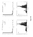
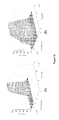
- the results are actually depicted in the histograms plotted in Figure 28 .
- the net capacitance report summarizes two values, a minimum and a maximum capacitance depending on the actual signal transition type at the net (e.g. rise or fall). Therefore two histograms Cmin and Cmax are computed associated to these two possible situations.
- Every Monte-Carlo run simulates all the 1714 vectors of the RTL test bench. Consequently, every Monte-Carlo run already accounts for the impact of the vector variation in the WA metric. Therefore the remaining variability that is observed in WA can only be due to extra switching activity which is not required to perform the logic functionality of the processor. Indeed this is attributed to unnecessary switching or glitches created by signals "travelling" the logic and converging at gates with unsynchronized timing.
- the amount for process induced activity variability can be very large. For the driver discussed, this results in a shift of the nominal activity toward a higher statistically expected value between 38% and 47% and a +/-3 ⁇ sigma spread between 32% and 34%.
- the final dynamic power figure for the complete SoC shows a shift of 35% for the statistical mean over the nominal value and a +/-3 ⁇ sigma spread of 30% of such mean. This clearly proves that for random WID variations, capacitance variations do not average linearly across the switching nodes of the die and thus do not have negligible impact on switching power when the impact on activity induced variability is not ignored.
- each component in the design has been statistically characterized. This characterization includes the statistical critical path and the power information, both active and leakage power.
- the goal of the architecture level yield analysis is to statistically estimate the timing and power consumption at the system level. Using these results it is possible to compare the system parametric timing/power against their specifications. Based on the activities of the connections and the nature, asynchronous or clocked, the statistical properties of the different logic blocks get combined.
- the Framework Module "Statistical standard cell library characterization” creates random cells based on the designers configuration for the compact model including V th variability and transistor gain ( ⁇ ) variability. These standard cells are simulated by the "Characterized standard-cell” module and this simulation creates the variability library for the next level.
- the Interface "create random logic Components" placed between the "Statistical standard cell library characterization” and the "Statistical digital characterization for standard-cell blocks” can be explained using a brick and wall analogy.
- the variability standard cell library can be thought of as a basket of a random set of bricks, one for each type of brick.
- the script implementing that interface randomly picks a brick instance out of a brick type basket. This brick is then randomly assigned to a brick of the same type in the random wall. This wall is in the present case the gate level netlist for the specified Component.
- the goal of the "Statistical digital characterization for standard-cell blocks" is to simulate gatelevel netlists (walls), preferably with any commercially available standard simulation and analysis tool.
- Static Timing Analysis (STA) tools exists for example the Prime Time tool from Synopsis or XT tool from Mentor Graphics.
- RTL Register Transfer Level
- These activities can be obtained by simulating the RTL implemented in the Hardware Description Language VHDL of the Architecture simulating a defined Application, as outlined in Figure 4 .
- the goal of this step is to obtain the correlated delay and power for the characterized gatelevel netlists under variability.
- the framework module "Statistical characterization of SoC architecture” catches the variability information for the complete SoC architecture providing feedback on system wide yield integration. Using the above simile of bricks and walls this step can be seen as building MC houses out of MC walls.
- FIG. 5 shows the architecture behind this framework. The algorithm will be described in detail below.
- the architecture for simulation is explained using the testbench framework for the architecture of the test vehicle. Such architecture corresponds to a real life design of a processor, hereafter called SyncProll. Still, this architecture is generic enough to accumulate any other application functionality for the SyncProll processor but also for different designs.
- the design of the processor which is used as input for the RTL module is a VLIW machine. This is a pipelined architecture with two fetch, a decode and two execute pipes.
- the simulation script e.g. the Modelsim script, is able to simulate the complete behaviour of the micro processor. This is possible, because Modelsim provides the functionality to load his memories with a particular file, which contains the application information in form of VLIW instructions.
- a testbench maps the test-vectors of the stimuli file, e.g. stim.dat file, to the input pins of the design.
- the Modelsim script receives as input the RTL VHDL sources of the architecture, configuration files, the testbench and the initialisation files for the memories in the architecture.
- the Modelsim scripts works in three steps. The first step is to compile the RTL VHDL sources of the architecture. The second step is to initialise the program memory based on information, captured by simulating the application opcode. The third step is to simulate the architecture by running the application testbench by reading the data value of the stimuli file, e.g. Stim.dat file.
- the activities are stored, e.g. the function "vcd dumpports" of Modelsim, writes the activities into the Value Change Dump (VCD) file.
- VCD Value Change Dump
- This is used to obtain the stimuli information for the Gatelevel simulation.
- the Components for which the activities are collected may be specified into a configuration file.
- the generated activity tracing file e.g. a vcd file, contains the bitvector set for the defined component in the architecture. If the designer changes the system architecture, only the following modifications need to be changed:
- the simulation flow shows the four MC loops, one for generating the variability netlists and the other three for analysis of the timing, activity and power, respectively.
- the "Create Random logical component” module creates the variability logical netlists based on the variability library obtained in level below in VAM. It also requires the original netlist of the block to be studied.
- the MC loop of the "Timing Analysis” module reads all existing variability netlists of the defined component and calculates the delay of the critical path capturing the delay for each cell.
- the module “Switching Activity” provides the transitions of each signal based on the stimuli simulation of the RTL simulation.
- the last MC loop calculates the power of each netlist based on the activity and timing information obtained in the previous modules.
- VAM VAM
- the heart of this VAM module is a script that creates random Netlists by using statistically characterized standard cells.
- the random netlist generator takes the nominal verilog netlist and uses the information of the Variability library to change the Cell names and modify the netlist file.
- a very straight forward solution could have been to simply concatenate a randomly generated number to the cell name found in the netlist.
- that cell instance may exist in the target variability cell library. Indeed sometimes a too high variation in the threshold voltage of a cell may lead to a non functional cell, therefore such cell is discarded from the variability library. If the randomly generated number refers to a cell that has been discarded it will therefore refer to a non existing cell in the library and this should be avoided.
- Possible solutions are outlined Figure 7a and Figure 7b .
- the Random Netlist Generator saves the different Cell names into a Hash table.
- the Cell name is the key to an extended list, where the different version numbers are saved. If the script finds the target Cell name in the hash table it uses a random key for the extended Hash table to obtain a version of the cell, which is then used to replace the target cell in the variability netlist.
- FIG. 7b an alternative implementation of the Random Netlist Generator avoiding the use of a hash table is shown.
- the nominal Cell name is the first key to a double list.
- the second key points to where the different version numbers have been saved.
- the script finds the target Cell name in the first list it uses a random key for accessing the second list to obtain a version of the cell, which is then used to exchange the target cell name in the variability netlist.
- FIG. 8a shows the input and output of the timing analysis tool.
- the script reads the synopsys design constraint (SDC) file which contains the timing/area or power constraints and clock, library, and load capacitance for primary output / input configuration of synthesis.
- the LIB file represents the variability library with the random type cells, which are used in the verilog netlist.
- the synopsys parasitic exchange (SPEF) file includes the parasitics obtained after physical design. This file is received after place and route for example with the commercial tool SoC-encounter. In this case VAM would simulate an architecture after place and route.
- the script uses then these inputs to calculate the timing file, e.g. SDF file, with the delay information of the cells and a timing report counting the delay of the critical path.
- FIG. 9a shows the script for the Activity Analysis.
- the tool Modelsim from Mentor Graphics may be used.
- the script reads the standard delay file, with the cell delays and their operation condition, the variability library and the MC netlist to simulate the MC gatelevel descriptions.
- the VITAL files and the netlist need to be compiled.
- This VITAL library represents the cell information of the LIB file in VHDL or verilog format. After this the logic simulation can be run.
- the switching activity file is created, e.g. a VCD file.
- This File Format is structured and it may be similar to the SAIF.
- the difference is the VCD file provides detailed information on activity per clock cycle to the SAIF file, which only gives total toggle count. It is possible to convert the VCD file to the SAIF file, if necessary, by using a commercial tool. Both files can be used for the power analysis, however, using a VCD file provides a more accurate result as it contains cycle true information (e.g. the actual waveform information instead just the total toggling count).
- a synopsys parasitic exchange file SPEF
- the back annotation netlist can be used in the simulation flow like a logical netlist.
- the power analysis tool can calculate the power report for each simulated component. Their are two different power calculations, that have to be summed up to reach the total power figure :
- the leakage power is the power consumed by the gate when inactive, hence when the gate does not switch. This is mostly due to leakage between source and drain, but may also be due to gate leakage.
- the third party power analysis tool may use for calculation of power the information of the library, which in embodiments of the present invention is the statistical standard library. The following calculations are assumed to be by the power analysis tool:
- Total power is shown in the power report as the summary of active power and leakage power.
- the histograms for power and/or energy can be calculated against timing curves and a comparison against the nominal design can be performed by using the functionality of the last module "Statistical characterization of SoC architectures".
- the CPU time efficiency of the characterization framework in accordance with embodiments of the present invention can be drastically speed-up by performing the task "create random logic component" (See Section 2.2.1 above) inside third party tools. Indeed by doing so the CPU time intensive task of unnecessarily re-parsing all over again each Monte Carlo is avoided. Indeed, this is a redundant task since all Monte Carlo netlist are structurally (e.g. topologically) the same, hence it is unnecessary to repeat a large part of the parsing effort (e.g. the circuit topology check and construction) over time. Instead this task can be performed by accessing and changing the reference of the netlist cell instance to a particular library cell element (a Monte Carlo standard cell). Figures 8b , 9b , 10b show how to adapt the different steps to implement this variant.
- Figure 11 a shows details of an implementation of a VAM Module according to embodiments of the present invention when creating variability netlists outside third party tools.
- the flow comprises generating a Monte Carlo (MC) set of netlists (see box Create Random Netlist) by following the process illustrated in Figure 7a or 7b which are later on, each of them, analyzed for their critical timing path (see box Timing Analysis); simulated at the logic level (see box Gatelevel simulation) and analyzed for power (see box Power Analysis).
- MC files are generated (see .v, for verilog, see .vcd, for value change dump, see .sdf, for standard delay format and see .saif for standard activity information format).
- Besides these intermediate files there is a second output of the flow in the form MC of timing and power reports in a non-standard format (see .rep files)
- Figure 11b shows details of an implementation of a VAM Module according to embodiments of the present invention when creating variability netlists inside third party tools.
- the process is done by making all needed analysis (e.g., analyzing the timing, performing the logic situation and analyzing the power) for each MC generated netlist before the next one is actually being produced.
- This saves intermediate storage by several orders of magnitude (from GBytes to Mbytes) and CPU time by avoiding the repetitive parsing of netlists which are topologically identical (see the different MC .v files of Figure 11a ).
- Figure 30 shows an implementation of the concept enabling such capability.
- test-vehicle is part of a software defined radio (SDR) being developed at IMEC. It comprises a synchronization engine for a baseband processor. This processor is the second generation of its nature designed at IMEC and is called hereafter SyncProll.
- SDR software defined radio
- results obtained in this chapter are based on the "Characterized standard-cell" script of the variability aware modeling in accordance with embodiments of the present invention.
- the output of this script is the statistical library.
- a synthesis flow is used to obtain the netlist of the design.
- the following sections discuss how to obtain the variability library and netlist of the design. The last section in this chapter compares the nominal design with the design effected by variability.
- the SyncProll is a pipelined synchronization processor. It is implemented in LISA and can be exported into an RTL VHDL description by using the Lisatek tool suite from Coware.
- the SyncProll itself is a part of an SDR architecture of a receiver for WLAN or WIMAX communications. The methodology is generic and can be adopted for other architectures as well.
- the principal functionality of the Testbench of the SyncProll is to find out a synchronization point in the data received by the antenna interface.
- This receiver obtains a set of specified preambles via the antenna of the receiver.
- the SyncProll architecture obtains the vectorised data from the antenna and verifies the correctness of the data.
- a file is used, which contains examples of data input. This information is specified via "Stim.dat" file, which includes the defined preambles data.
- the next block (see Figure 12 ) vectorises this information, saves it to a Circular Buffer and sends this to the SyncProll architecture including a signal that indicates the processor is ready to resume the operation. This resume signal wakes up the processor and starts the application which evaluates the preambles.
- the functionality performed by the processor is the accumulation of these preambles to verify a specified threshold. By adding up these vectors a ramp function is obtained. After a defined amount of preambles the ramp reaches a specified value.
- the first correct value of these preambles is the output of the processor and provides the pointer to a circular buffer that queues the data.
- the behavior of the specified component or of the complete architecture can be simulated.
- the designer has to provide a synthesis flow to obtain the logical or physical netlist.
- the designer can increase the accuracy of the simulation flow by providing a netlist after place and route including the SPEF file.
- the logical synthesis will be described.
- the synthesis flow used for the SyncProll is shown in the Figure 13 .
- the input for the synthesis tool is the architecture written in a hardware description language such as verilog or VHDL.
- VHDL hardware description language
- a synthesis step needs to be performed to obtain a gate-level VHDL or Verilog description in terms of logical netlist or a boolean equation representation of the combinational logic.
- This logical netlist includes the behavior of the VHDL code in gatelevel format. Obeying constraints, specified by the designer, the synthesis tool is able to optimize for area and/or timing.
- Figure 13 shows a design optimized with three different constraint settings.
- the first setting selects optimisations to achieve a minimum delay design.
- setting 3 selects optimisation for an area optimized design (minimum power) with maximum delay.
- setting 2 selects an intermediate trade-off constraint to a timing in between the minimum and maximum achievable delay. In the case illustrated it is considered to optimize to the minimum possible delay to investigate the impact in parametric timing yield, shown in Figure 13 as the upper point in the graph, by setting the maximum target delay constraint to zero.
- the synthesis tool uses for this optimisation the delay, area and power information of the cells in the nominal library. After optimisation the nominal Gatelevel netlist with the nominal cells of the library is obtained.
- Figure 14 represents the delay and internal dynamic Power histogram of standard cells during gate activation.
- Figure 15 shows the delay and internal total Power histogram of standard cells considering leakage effects.
- the total power is the addition of active and leakage power.
- the results of the gatelevel simulation are the switching activity files for each netlist.
- the files include the active and the inactive time of the signals of the logic block and the transition of the signals.
- a more relevant figure of merit is to account for the activity of each net weighted by the corresponding net capacitance.
- Such metric gives an idea of the variation in dynamic power. Indeed this is the case as dynamic power directly relates to the sum of toggling activity in each net multiplied by the total lumped capacitance in that net (besides other proportional factors as supply voltage and clock frequency).
- Such capacitance can be obtained as a report of either the timing analysis and/or power analysis tool.
- the "VALU_VECTOR0" component of the execute pipe in the SyncProll architecture is shown as example.
- the "VALU_VECTOR0" netlist contains 11000 cells. The cell count between components ranges from 350 for the "STORE_DE” memory storage unit to 49000 cells for the "CMUL_EX_VECTOR0" complex multiplier unit.
- the "VALU_VECTOR0” unit includes the vector arithmetic logic unit functionality MOVE, ADD, AND, SHIFT, SUB and OR operation for vectors and is therefore above the average complexity in comparison to other components of the architecture. Power has been calculated for the vector exciting the critical path of the component.
- Figure 17a,b,c show the histograms for active, leakage and total power of the "VALU_VECTOR0" block of the SyncProll processor, which shows a mean of 2 mili Watt spreading from 1 till 2.4 mili Watt variation for Power, such spread mainly due to active power. This shows a variation of 70% in Power. This value is calculated by using the statistical standard cells without any wire load model and does not consider the actual load of the component within the architecture.
- Figure 18 shows a histogram for delay of the "VALU_VECTOR0" block of the SyncProll processor, which shows a mean in delay of about 0.6 nano seconds with a spread up to 1.5 nano seconds standard. This shows a variation of 150% in delay.
- Figures 19, 20 and 21 show the delay and energy histograms in comparison with the nominal design, indicated in these Figures by a line.
- the designer is able to see the energy and delay curve for each component in the system.
- the nominal line is calculated as the maximum delay of all the nominal values for each component.
- the components at the right side of the nominal line are statistically slower than the excepted nominal design. This is thus an indication to the designer for speed bottlenecks under variability.
- the designer can change constraints to optimize the components to redo the top-down synthesis flow.
- the power is calculated this time for vectors obtained from the RTL
- Theload of the component in the system is not included in the characterization. This means that the components are simulated with the assumption that they have nothing to drive. Similarly they are assumed to be ideally driven. Every input/output of the different components has no specified driving/load conditions even if other components are connected to/from it. More accurate information is obtained if components are characterized considering the actual driving and load conditions they have. This can be done via the information contained in the Synthesis Design Constraint file and feeding this file to the timing and power analysis tools as shown in Figures 8a, 8b , 10a, 10b , 11 a , 11 b .
- Figures 20 and 21 show the active and the leakage Energy consumption of each block and the nominal active and leakage energy value of the SyncProll excluding the register files and memories. The designer can locate, which component has the highest leakage energy or the highest active energy consumption. Depending on the problem, the logic block can be modified for example to reduce leakage by increasing transistor length or properly shutting down gates by properly controlling the introducing sleep transistors present in the cell.
- VAM flow in accordance with embodiments of the present invention is the overview of the curves for delay, active and leakage Power in comparison with the nominal design.
- the designer can check the mean shift to the architecture nominal value but also the comparison component nominal value and component variability mean value and distribution.
- the whole architecture can be simulated excluding memories and registers.
- the digital characterization loop can also be used to characterize the complete flattened netlist of the SyncProll instead of its components.
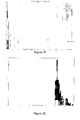
- the simulation results of a complete architecture Of the SyncProll, excluding memories and registers, are shown in Figures 22 to 25 .
- the nominal value for the characterized pipe is not the same as in the previous section.
- the reason (mentioned in the previous section) is the missing drive/load information for each component assumed when the component alone was characterized. In case of using the pipe flattened description these drive/load conditions are implicitly included. It is also to be mentioned that a significant shift is observed of the mean of the characterized architecture affected by variability and the nominal value for delay (36%), active power (20%), and total power (10%). The shift in power increases when considering about the 1000 vectors resulting from the RTL simulation, reporting shifts up to 46% for total power.
- Figure 26 shows the results of the characterized "VALU_VECTOR0" block of the SyncProll architecture by using different amounts of MC loops.
- Figure 26 shows a mean shift of power and delay and also an increase of the spread depending on the MC count.
- Another aspect is how accurately outliers can be captured. These outliers or extreme values are critical values outside of the bulk of the distribution.
- percentiles the amount of outliers captured by the different MC runs can be quantified, as shown in Table I. The percentile are calculated for X% of the population starting from maximum value. The table shows the percentile for 0.1 %, 1 % and 10% of delay, active and total power. By using the 0.1 % percentile for delay we can see a strong increasing of maximum delay of about 18%. In case of the total and dynamic Power we have a increase for about 1 % of outliers.
- VAM scheme One of the advantages of the VAM scheme according to embodiments of the present invention is the possibility to simulate random events not part of the main statistical distribution. This is exactly where any analytical method not assisted by Monte Carlo analysis would fail.
- Such NAND gates had approximately ten times more gate delay than the nominal gate and it was obtained by statistical simulation at the gate (analog) level by injecting a random process in the threshold voltages of the transistors of the gate netlist that were characterised by a gaussian process with a standard deviation of roughly ten times bigger than the standard deviation used to simulate the statistical gates following the "normal" statistical distribution.
- Figure 27 and Table II show the outcome of the experiment. Any statistical analysis tool would report the histogram indicated by reference number 270 as opposed to the histograms 271, 272 obtained via VAM simulation in accordance with embodiments of the present invention.
- the flow described above may be used to guide existing or future optimization tools that, although not being variability aware, have the goal to change and/or introduce new elements in such netlist with the purpose of changing the energy/delay parametric characteristics of the circuit.
- Such tools having as input a (back-annotated) netlist of the circuit in terms of standard cells and/or the transistor level view of such standard cells and a library of such standard cells, share the same input information as the VAM flow. Therefore the flow described here may be used after the optimization phase to provide feedback to these tools on the impact of their decisions in the energy/delay/yield metrics of the circuit under variability.
- the flow described in this patent shall enable such tools taking the optimal trade-off decision while accounting for the process variability effects in energy/delay and yield.
- One example of such optimizing goals is the step of allocating transistors with different threshold voltages in a netlist to reduce leakage power.
- Such allocation affects the timing of the paths in the netlist and given such timing is statistically affected by variability it may create more or other paths that become statistically critical than in nominal condition (e.g. not affected by variability), hence affecting yield.
- VAM flow according to embodiments of the present invention allows to estimate the energy, the timing and the yield of the circuit in statistical conditions, the flow will guide the selection process of the threshold voltage with minimal impact on yield.
- the variability modeling flow according to the second embodiment of the present invention is depicted in Figure 29 . It starts from information about the impact of process variability in device compact models (such as BSIM) and from a complementary set of variability scaling rules based on measurement data, data estimated by TCAD simulations or ITRS trends. A similar approach is taken for passives and interconnects (R, C). Such "rules” include models about how variability affects transistors of different gate lengths or widths, such as Pelgrom's mismatch model for FETs.
- the flow according to the second embodiment is divided into two interleaved subflows: a variability injection flow comprising boxes (1) and (3) at the left hand side of Figure 29 and a simulation/analysis flow comprising boxes (2) and (4) at the right hand side of Figure 2 .
- a fully analytical technique (described in EP-07075505.3 ) integrates in box (5) the correlated power/delay variations from each of the SoC subcomponents to obtain the unified SoC level statistics in the form of a trade-off model between SoC level design metrics such as parametric yield, clock frequency and power.
- FIG. 30 The flow for this digital analyis/simulation is illustrated in Figure 30 . It is based on a matlab script as master process controlling two slave Synopsys DC-shell and Mentor Graphics Modelsim processes.
- the Synopsys DC-shell process serves the purpose of providing conventional static timing analysis and standard power analysis capabilities to the flow.
- the Mentor Graphics Modelsim process provides standard time sensitive logic simulation capabilities.
- the standard static timing analysis results in a delay format report, e.g. a standard delay format report ( .sdf) and critical path for each Verilog netlist which are then fed into the logic simulator resulting in value change dump report for activity (.vcd) which is then analyzed by a power analysis tool for final reporting on dynamic and leakage power consumptions.
- a delay format report e.g. a standard delay format report ( .sdf) and critical path for each Verilog netlist which are then fed into the logic simulator resulting in value change dump report for activity (.vcd) which is then analyzed
- the simulation flow may build on top of mainstream commercial EDA analysis tools and simulators. For example, it may be built on top of Mentor Graphics's Modelsim simulator (for RTL and gate level simulation) and on top of Synopsys's PrimeTime and PrimePower analysis tools for static timing and power analysis purposes.
- a Matlab script around these third party tools may implement a Monte-Carlo based methodology.
- the implementation of the flow may be tuned to make Matlab code to direclty interact with the API interfaces of the third party tools to avoid unnecessary reparsing of the topologically identical Verilog netlists.
- timing may be analysed, a logic simulation may be performed and power may be analysed with an average of 2K gate per second per simulation including 2K vector logic simulation. Indeed, 200 iterations of a flow according to the second embodiment for a 120K-gate test vehicle may take less than 4 hours.
- the analysis at the integration level may actually be performed hierarchically. If the components are so large that digital simulation becomes too time consuming, the digital level analysis flow (box 4 of Figure 29 ) may be applied to the sub-parts of the SoC components and then the component level results may be obtained using this technique. This can be done on condition the SoC component is broken up at places where register boundaries exists (see EP-07075505.3 ), for instance the logic between pipeline stage in a processor (see experimental results below). At the integration stage it can applied to bring together all top-level component statistical properties.
- leakage power has been transformed into leakage energy by assuming a clock cycle equal to the longest path delay and considering the SoC requires 1714 of these cycles to complete one symbol synchronization. This is indeed the total simulation time considered for the calculation of dynamic energy during logic simulation. Similarly we can proceed to transform dynamic energy into dynamic power disipation but this time dividing energy by the total simulation time.
- Figure 32 shows the less intuitive statistical correlation between timing and power (both dynamic and leakage).
- the SoC's yield is evaluated as a function of its specifications, which are expressed as clock frequency, power budget, but also others as supply voltage range, temperatures range, etc.
- Figure 31 shows the yield (expressed as the Cumulative Density Function) for each of the device options at the full VLIW processor level.
- This aspect of the invention relates to method for the insertion of digital and/or analog monitors in the digital circuits where this is done before synthesis, hence at the RTL level, as opposed to all other described techniques where this is done after synthesis, hence at the netlist level.
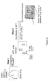
- the method comprises two steps as illustrated in Figure 1 .
- a delay monitor senses the position of an edge of a combinational logic output relative to the clock edge that controls the corresponding FlipFlop (FF). Therefore the goal of Step 1 of the flow is to identify in the RTL code these places where the synthesis tool will infer sequential logic. Such places are easily recognized in the code whenever an assignment to a signal or variable takes place conditional to waiting for a clock event. Indeed a property of RTL is that there exists a one-to-one mapping between such constructs of the code and the inferred FFs. The actual syntax depends on the language used to describe the RTL functionality. However, the mechanism is essentially the same in both languages.
- the Right Hand Side (signal_RHS) of the statement corresponds to the output of the path of the combinational logic that will be monitored (D port of the inferred FF); while the Left Hand Side (signal_LHS) corresponds to the output of the inferred FF (Q port of such FF).
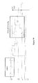
- the delay monitor must connect in parallel to the inferred FF (see Figure 36 ) in such way that the combinational logic output (signal_LHS) serves as input to both the FF and the delay monitor. This may be done by enforcing a port assignment (or port mapping in VHDL) between both the left hand side of the statement (signal_LHS) and the D-input of the delay monitor.
- the next step is to perform both logic synthesis and scan chain insertion phases.
- no special care needs to be taken during synthesis.
- some care must be taken during the scan chain insertion phase (part of the Design For Testability or DFT flow).
- additional scan chains besides the ones dedicated to testing purposes must be created during the synthesis script to service the monitors.
- a digital delay monitor is to detect any 'significant' shifts in delay of the combinational logic whose outputs shall be connected to the data input of a latch or FlipFlop (FF) of any type (e.g., rising-edge-triggered flip-flop, falling-edge-triggered flip-flops, latches, etc) inferred by the RTL synthesis tool.
- FF FlipFlop
- the output of the latch is then captured by a FF that will serve the purpose of being part of a scan chain that will take the monitor bits to a known location in the chip and/or the outside world for subsequent analysis.
- the power impact of the delay element is small since the activity factor of the combinational logic output is lower than the clock. Moreover, if the aging sensors are mostly turned off and are turned on as and when required, then the power impact will be very small as well.
- the delay monitor When the slack is violated due to a timing degradation of the monitored path (e.g. due to process variations, aging, temperature gradients, IR induced voltage drops or any other physical mechanism), the delay monitor will report a fault in the form of a Boolean output. Moreover, the information carried on by the Boolean output in combination with a controlled sweeping of the clock frequency can be used to measure the actual absolute timing of the critical path of the device. The accuracy of such measurement shall be equal to the delay introduced by delay line that is found inside the delay monitor. Because the Boolean just indicates a particular monitored path that is about to suffer from a timing violation but not yet, that path and the rest of the device paths remain still functional, hence facilitating a successful read out of the monitoring information.
- This approach enables runtime gathering of information concerning the impact of ageing and/or process variations at the circuit level. Such information can be advantageous to calibrate higher level models of the system. When repeated over a number of samples such information shall be used to calibrate statistical models of the subsystems of the device being sensed.
- the delay monitor behavior can be described at the RTL level. See Appendix B for details.
- Monitors of analog nature such as voltage, current, energy or temperature monitors between others can be also introduced at the RTL by following the techniques described in Section 6.2.
- the description of such monitor will differ from the delay monitor. Given the analog nature of the monitor, such description will serve the purpose of allowing a behavioral simulation of the complete digital device at the RTL level.
- Such monitor shall become part of the available design library as a cell or a macro cell.
- Specific constructs such as: map to operator (see Synopsys' DC-shell manual for description) will be part of the RTL description of such monitor to instruct the synthesis tool to select a pre-designed cell of the library where such behavioral description shall be mapped to.
- map to operator see Synopsys' DC-shell manual for description
- direct mapping capabilities from the RTL to a selected component in the library are also available (see vendor specific manuals).
- Such analog monitor will have at the output the same combination of latch and FF such as that one being found in Figure 36 to allow scan chain routing capabilities.
Landscapes
- Engineering & Computer Science (AREA)
- Computer Hardware Design (AREA)
- Physics & Mathematics (AREA)
- Theoretical Computer Science (AREA)
- Evolutionary Computation (AREA)
- Geometry (AREA)
- General Engineering & Computer Science (AREA)
- General Physics & Mathematics (AREA)
- Design And Manufacture Of Integrated Circuits (AREA)
Applications Claiming Priority (1)
| Application Number | Priority Date | Filing Date | Title |
|---|---|---|---|
| US94589907P | 2007-06-22 | 2007-06-22 |
Publications (1)
| Publication Number | Publication Date |
|---|---|
| EP2006784A1 true EP2006784A1 (de) | 2008-12-24 |
Family
ID=39777024
Family Applications (1)
| Application Number | Title | Priority Date | Filing Date |
|---|---|---|---|
| EP08158713A Withdrawn EP2006784A1 (de) | 2007-06-22 | 2008-06-20 | Verfahren zur Charakterisierung elektronischer Schaltungen unter Prozessvariabilitätseffekten |
Country Status (2)
| Country | Link |
|---|---|
| US (2) | US8286112B2 (de) |
| EP (1) | EP2006784A1 (de) |
Cited By (24)
| Publication number | Priority date | Publication date | Assignee | Title |
|---|---|---|---|---|
| EP2662791A1 (de) * | 2012-05-11 | 2013-11-13 | Stichting IMEC Nederland | Verfahren und Vorrichtung zur Überwachung des Timings kritischer Pfade |
| EP2899654A1 (de) * | 2014-01-28 | 2015-07-29 | IMEC vzw | Verfahren, System und Computerprogrammprodukt zur Charakterisierung der Variabilität eines Entwurfs einer integrierten Schaltung |
| WO2019244154A1 (en) | 2018-06-19 | 2019-12-26 | Proteantecs Ltd. | Efficient integrated circuit simulation and testing |
| US10621296B1 (en) | 2017-06-07 | 2020-04-14 | Synopsys, Inc. | Generating SAIF efficiently from hardware platforms |
| US11385282B2 (en) | 2017-11-15 | 2022-07-12 | Proteantecs Ltd. | Integrated circuit margin measurement and failure prediction device |
| US11391771B2 (en) | 2017-11-23 | 2022-07-19 | Proteantecs Ltd. | Integrated circuit pad failure detection |
| US11408932B2 (en) | 2018-01-08 | 2022-08-09 | Proteantecs Ltd. | Integrated circuit workload, temperature and/or subthreshold leakage sensor |
| US11475195B2 (en) * | 2017-04-28 | 2022-10-18 | Samsung Electronics Co., Ltd. | Computer-implemented method and computing system for designing integrated circuit by considering timing delay |
| US20230142132A1 (en) * | 2021-11-10 | 2023-05-11 | Realtek Semiconductor Corp. | Method for establishing variation model related to circuit characteristics for performing circuit simulation, and associated circuit simulation system |
| US11740281B2 (en) | 2018-01-08 | 2023-08-29 | Proteantecs Ltd. | Integrated circuit degradation estimation and time-of-failure prediction using workload and margin sensing |
| US11762789B2 (en) | 2018-12-30 | 2023-09-19 | Proteantecs Ltd. | Integrated circuit I/O integrity and degradation monitoring |
| US11762013B2 (en) | 2018-04-16 | 2023-09-19 | Proteantecs Ltd. | Integrated circuit profiling and anomaly detection |
| US11815551B1 (en) | 2022-06-07 | 2023-11-14 | Proteantecs Ltd. | Die-to-die connectivity monitoring using a clocked receiver |
| US11861281B2 (en) * | 2017-04-28 | 2024-01-02 | Samsung Electronics Co., Ltd. | Computer-implemented method and computing system for designing integrated circuit by considering timing delay |
| US11929131B2 (en) | 2019-12-04 | 2024-03-12 | Proteantecs Ltd. | Memory device degradation monitoring |
| US12013800B1 (en) | 2023-02-08 | 2024-06-18 | Proteantecs Ltd. | Die-to-die and chip-to-chip connectivity monitoring |
| US12072376B2 (en) | 2020-04-20 | 2024-08-27 | Proteantecs Ltd. | Die-to-die connectivity monitoring |
| US12123908B1 (en) | 2023-09-12 | 2024-10-22 | Proteantecs Ltd. | Loopback testing of integrated circuits |
| US12241933B2 (en) | 2020-07-06 | 2025-03-04 | Proteantecs Ltd. | Integrated circuit margin measurement for structural testing |
| US12282058B2 (en) | 2017-11-23 | 2025-04-22 | Proteantecs Ltd. | Integrated circuit pad failure detection |
| WO2025085076A1 (en) * | 2023-10-17 | 2025-04-24 | Siemens Industry Software Inc. | Evaluating power dissipation |
| US12461143B2 (en) | 2024-01-24 | 2025-11-04 | Proteantecs Ltd. | Integrated circuit margin measurement |
| US12470223B2 (en) | 2021-04-07 | 2025-11-11 | Proteantecs Ltd. | Adaptive frequency scaling based on clock cycle time measurement |
| US12481811B1 (en) * | 2022-12-05 | 2025-11-25 | Cadence Design Systems, Inc. | Circuit design modification based on timing tradeoff |
Families Citing this family (82)
| Publication number | Priority date | Publication date | Assignee | Title |
|---|---|---|---|---|
| GB2443277B (en) * | 2006-10-24 | 2011-05-18 | Advanced Risc Mach Ltd | Performing diagnostics operations upon an asymmetric multiprocessor apparatus |
| CN102768696B (zh) * | 2007-03-09 | 2017-04-26 | 明导公司 | 增量式布局分析 |
| EP2006784A1 (de) * | 2007-06-22 | 2008-12-24 | Interuniversitair Microelektronica Centrum vzw | Verfahren zur Charakterisierung elektronischer Schaltungen unter Prozessvariabilitätseffekten |
| US20090013292A1 (en) * | 2007-07-03 | 2009-01-08 | Mentor Graphics Corporation | Context dependent timing analysis and prediction |
| US7991577B2 (en) | 2007-08-30 | 2011-08-02 | HSB Solomon Associates, LLP | Control asset comparative performance analysis system and methodology |
| US7752585B2 (en) * | 2007-10-15 | 2010-07-06 | International Business Machines Corporation | Method, apparatus, and computer program product for stale NDR detection |
| US8245084B2 (en) * | 2008-01-11 | 2012-08-14 | International Business Machines Corporation | Two-level representative workload phase detection |
| US8204730B2 (en) * | 2008-06-06 | 2012-06-19 | Synopsys, Inc. | Generating variation-aware library data with efficient device mismatch characterization |
| US8825464B2 (en) * | 2008-09-02 | 2014-09-02 | Oracle America, Inc. | Method and apparatus for parallelization of sequential power simulation |
| JP2010160787A (ja) * | 2008-12-11 | 2010-07-22 | Jedat Inc | パラメータ情報作成システム、歩留まり算出システム、プログラム及び記録媒体 |
| US8161434B2 (en) * | 2009-03-06 | 2012-04-17 | Synopsys, Inc. | Statistical formal activity analysis with consideration of temporal and spatial correlations |
| US8201137B1 (en) * | 2009-03-06 | 2012-06-12 | Cadence Design Systems, Inc. | Method and apparatus for AMS simulation of integrated circuit design |
| US20100250187A1 (en) * | 2009-03-25 | 2010-09-30 | Imec | Method and system for analyzing performance metrics of array type circuits under process variability |
| US8122411B2 (en) * | 2009-07-16 | 2012-02-21 | International Business Machines Corporation | Method of performing static timing analysis considering abstracted cell's interconnect parasitics |
| DE102009034242A1 (de) * | 2009-07-22 | 2011-01-27 | Volkswagen Ag | Verfahren und Vorrichtung zum Prüfen eines Steuergeräts eines Fahrzeugs |
| US9684742B1 (en) * | 2009-08-26 | 2017-06-20 | Altera Corporation | Method and apparatus for performing timing analysis on calibrated paths |
| JP5445066B2 (ja) * | 2009-11-25 | 2014-03-19 | 富士通株式会社 | 解析支援プログラム、解析支援装置、および解析支援方法 |
| US8924902B2 (en) * | 2010-01-06 | 2014-12-30 | Qualcomm Incorporated | Methods and circuits for optimizing performance and power consumption in a design and circuit employing lower threshold voltage (LVT) devices |
| US20110181331A1 (en) * | 2010-01-24 | 2011-07-28 | Freescale Semiconductor, Inc. | Integrated circuit with leakage reduction in static nets |
| US8407646B2 (en) * | 2010-02-11 | 2013-03-26 | Synopsys, Inc. | Active net and parasitic net based approach for circuit simulation and characterization |
| US8266569B2 (en) * | 2010-03-05 | 2012-09-11 | Advanced Micro Devices, Inc. | Identification of critical enables using MEA and WAA metrics |
| JP5370256B2 (ja) * | 2010-05-06 | 2013-12-18 | 富士通株式会社 | 解析支援プログラム、解析支援装置および解析支援方法 |
| JP2011237989A (ja) * | 2010-05-10 | 2011-11-24 | Toshiba Corp | 半導体集積回路の設計装置、その設計方法、及びその設計プログラム |
| US8515724B2 (en) * | 2010-06-22 | 2013-08-20 | International Business Machines Corporation | Technology computer-aided design (TCAD)-based virtual fabrication |
| DE112011102691B4 (de) * | 2010-08-09 | 2019-05-09 | Charter Ip Llc | Verfahren und System zur Umwandlung von Zeitsteuerungsberichten in Zeitsteuerungswellenformen |
| US9208271B1 (en) * | 2010-11-19 | 2015-12-08 | Cadence Design Systems, Inc. | Transaction correlation system |
| US8522182B2 (en) * | 2011-03-21 | 2013-08-27 | International Business Machines Corporation | Generation of an end point report for a timing simulation of an integrated circuit |
| US9235675B2 (en) * | 2011-04-01 | 2016-01-12 | Taiwan Semiconductor Manufacturing Company, Ltd. | Multidimensional monte-carlo simulation for yield prediction |
| US20120266123A1 (en) * | 2011-04-12 | 2012-10-18 | Texas Instruments Incorporated | Coherent analysis of asymmetric aging and statistical process variation in electronic circuits |
| US8555210B2 (en) | 2011-04-29 | 2013-10-08 | Micron Technology, Inc. | Systems and methods for stochastic models of mask process variability |
| US8811068B1 (en) | 2011-05-13 | 2014-08-19 | Suvolta, Inc. | Integrated circuit devices and methods |
| US8397197B1 (en) | 2011-05-25 | 2013-03-12 | Applied Micro Circuits Corporation | Integrated circuit module time delay budgeting |
| US20130046912A1 (en) * | 2011-08-18 | 2013-02-21 | Maxeler Technologies, Ltd. | Methods of monitoring operation of programmable logic |
| US9355000B1 (en) * | 2011-08-23 | 2016-05-31 | The Mathworks, Inc. | Model level power consumption optimization in hardware description generation |
| US8392860B1 (en) | 2011-09-01 | 2013-03-05 | Apple Inc. | Identifying speed binning test vectors during simulation of an integrated circuit design |
| US8650519B2 (en) * | 2011-09-01 | 2014-02-11 | Apple Inc. | Automated functional coverage for an integrated circuit design |
| US8499274B2 (en) * | 2011-11-30 | 2013-07-30 | Taiwan Semiconductor Manufacturing Co., Ltd. | Computer implemented system and method for leakage calculation |
| US8819603B1 (en) | 2011-12-15 | 2014-08-26 | Suvolta, Inc. | Memory circuits and methods of making and designing the same |
| US8739094B2 (en) * | 2011-12-22 | 2014-05-27 | Lsi Corporation | Power estimation using activity information |
| US8543953B2 (en) | 2012-01-04 | 2013-09-24 | Apple Inc. | Automated stimulus steering during simulation of an integrated circuit design |
| US8522181B2 (en) | 2012-01-24 | 2013-08-27 | Synopsys, Inc. | Capacitance extraction for advanced device technologies |
| US9183330B2 (en) * | 2012-01-31 | 2015-11-10 | Mentor Graphics Corporation | Estimation of power and thermal profiles |
| US8413095B1 (en) * | 2012-02-21 | 2013-04-02 | International Business Machines Corporation | Statistical single library including on chip variation for rapid timing and power analysis |
| US9411921B2 (en) | 2012-04-27 | 2016-08-09 | Globalfoundries Inc. | FET-bounding for fast TCAD-based variation modeling |
| US8589842B1 (en) * | 2012-11-09 | 2013-11-19 | International Business Machines Corporation | Device-based random variability modeling in timing analysis |
| US9977849B2 (en) * | 2013-01-09 | 2018-05-22 | Nxp Usa, Inc. | Method and apparatus for calculating delay timing values for an integrated circuit design |
| US8819605B1 (en) * | 2013-03-06 | 2014-08-26 | Oracle International Corporation | Deriving effective corners for complex correlations |
| US9038006B2 (en) * | 2013-04-30 | 2015-05-19 | Freescale Semiconductor, Inc. | Method and apparatus for generating gate-level activity data for use in clock gating efficiency analysis |
| JP6111880B2 (ja) * | 2013-06-11 | 2017-04-12 | 富士通株式会社 | 検証支援方法、検証支援プログラム、および検証支援装置 |
| CN104598659B (zh) | 2013-10-31 | 2018-09-18 | 格芯公司 | 对数字电路进行仿真的方法和设备 |
| US9817931B1 (en) | 2013-12-05 | 2017-11-14 | The Mathworks, Inc. | Systems and methods for generating optimized hardware descriptions for models |
| US10078717B1 (en) | 2013-12-05 | 2018-09-18 | The Mathworks, Inc. | Systems and methods for estimating performance characteristics of hardware implementations of executable models |
| US9262569B2 (en) | 2014-02-20 | 2016-02-16 | Globalfoundries Inc. | Balancing sensitivities with respect to timing closure for integrated circuits |
| US9311444B1 (en) * | 2014-07-10 | 2016-04-12 | Sandia Corporation | Integrated circuit test-port architecture and method and apparatus of test-port generation |
| US9760672B1 (en) | 2014-12-22 | 2017-09-12 | Qualcomm Incorporated | Circuitry and method for critical path timing speculation to enable process variation compensation via voltage scaling |
| US9710590B2 (en) * | 2014-12-31 | 2017-07-18 | Arteris, Inc. | Estimation of chip floorplan activity distribution |
| KR102324782B1 (ko) * | 2015-01-22 | 2021-11-11 | 삼성전자주식회사 | 집적 회로의 정적 타이밍 분석 방법 |
| US20160283629A1 (en) | 2015-03-27 | 2016-09-29 | Imec Vzw | Complexity-reduced simulation of circuit reliability |
| US9564884B1 (en) * | 2015-04-13 | 2017-02-07 | Qualcomm Incorporated | Circuitry and method for measuring negative bias temperature instability (NBTI) and hot carrier injection (HCI) aging effects using edge sensitive sampling |
| US9564883B1 (en) * | 2015-04-13 | 2017-02-07 | Qualcomm Incorporated | Circuitry and method for timing speculation via toggling functional critical paths |
| US9536038B1 (en) | 2015-04-13 | 2017-01-03 | Qualcomm Incorporated | Method and algorithm for functional critical paths selection and critical path sensors and controller insertion |
| US9507891B1 (en) | 2015-05-29 | 2016-11-29 | International Business Machines Corporation | Automating a microarchitecture design exploration environment |
| US9697310B2 (en) * | 2015-11-02 | 2017-07-04 | Winbond Electronics Corporation | Level faults interception in integrated circuits |
| US10375325B2 (en) * | 2016-06-23 | 2019-08-06 | Fluke Corporation | Thermal anomaly detection |
| US10185795B1 (en) | 2016-10-11 | 2019-01-22 | Cadence Design Systems, Inc. | Systems and methods for statistical static timing analysis |
| US10073934B1 (en) * | 2016-10-11 | 2018-09-11 | Cadence Design Systems, Inc. | Systems and methods for statistical static timing analysis |
| EP4068142A1 (de) * | 2016-12-23 | 2022-10-05 | Google LLC | Appareil et procède pour la conception d'un circuit intégré |
| US10732703B2 (en) | 2017-03-02 | 2020-08-04 | Futurewei Technologies, Inc. | Apparatus and method for reducing an energy consumption of hardware based on an application state |
| CN108694261A (zh) * | 2017-04-10 | 2018-10-23 | 中国石油天然气股份有限公司 | 设备模型的构建方法及装置 |
| US10546095B2 (en) | 2017-06-13 | 2020-01-28 | International Business Machines Corporation | Parameter collapsing and corner reduction in an integrated circuit |
| US11113442B2 (en) * | 2017-09-28 | 2021-09-07 | Intel Corporation | Methods and apparatus for reducing reliability degradation on an integrated circuit |
| TWI681311B (zh) * | 2018-04-27 | 2020-01-01 | 瑞昱半導體股份有限公司 | 電路設計系統與檢查方法 |
| CN109101239B (zh) * | 2018-08-30 | 2021-09-14 | 杭州电子科技大学 | 一种在线Verilog代码自动判决系统的标准答案生成方法 |
| TWI697797B (zh) * | 2018-11-08 | 2020-07-01 | 瑞昱半導體股份有限公司 | 決定積體電路之電壓以及找出電壓與電路參數之關係的方法 |
| US10796046B2 (en) * | 2019-01-18 | 2020-10-06 | Mentor Graphics Corporation | Machine learning-based parasitic extraction automation for circuit design and verification |
| US11580356B2 (en) * | 2019-07-19 | 2023-02-14 | Qualcomm Incorporated | Efficient inferencing with piecewise pointwise convolution |
| US11763046B2 (en) * | 2019-11-05 | 2023-09-19 | Autodesk, Inc. | Techniques for automatically selecting simulation tools for and performing related simulations on computer-generated designs |
| US11126769B2 (en) * | 2020-02-04 | 2021-09-21 | Applied Materials, Inc. | Unified material-to-systems simulation, design, and verification for semiconductor design and manufacturing |
| US11275883B2 (en) | 2020-02-12 | 2022-03-15 | Siemens Industry Software Inc. | Machine learning-based classification in parasitic extraction automation for circuit design and verification |
| CN114239436B (zh) * | 2021-12-28 | 2025-07-08 | 中山大学 | 一种随机分布疏水点的池沸腾数值模拟方法 |
| US11842132B1 (en) * | 2022-03-09 | 2023-12-12 | Synopsys, Inc. | Multi-cycle power analysis of integrated circuit designs |
| EP4718179A1 (de) * | 2024-09-26 | 2026-04-01 | Siemens Aktiengesellschaft | Computerimplementiertes verfahren zur bestimmung eines ertrags eines herstellungsprozesses zur herstellung eines produkts |
Citations (4)
| Publication number | Priority date | Publication date | Assignee | Title |
|---|---|---|---|---|
| US20040122642A1 (en) * | 2002-12-23 | 2004-06-24 | Scheffer Louis K. | Method for accounting for process variation in the design of integrated circuits |
| US20050204316A1 (en) * | 2005-01-27 | 2005-09-15 | Chipvision Design Systems Ag | Predictable design of low power systems by pre-implementation estimation and optimization |
| EP1583009A1 (de) * | 2004-03-30 | 2005-10-05 | Interuniversitair Micro-Elektronica Centrum | Verfahren und Vorrichtung zum Entwerfen und Herstellen von elektronischen Schaltungen abhängig von Prozessveränderungen |
| EP1873665A1 (de) | 2006-06-28 | 2008-01-02 | Interuniversitair Microelektronica Centrum | Verfahren zur Untersuchung der Durchführbarkeit des Entwurfs eines elektronischen Systems |
Family Cites Families (8)
| Publication number | Priority date | Publication date | Assignee | Title |
|---|---|---|---|---|
| US6888564B2 (en) | 2002-05-24 | 2005-05-03 | Koninklijke Philips Electronics N.V. | Method and system for estimating sharpness metrics based on local edge kurtosis |
| US6880136B2 (en) | 2002-07-09 | 2005-04-12 | International Business Machines Corporation | Method to detect systematic defects in VLSI manufacturing |
| JP2004252831A (ja) * | 2003-02-21 | 2004-09-09 | Matsushita Electric Ind Co Ltd | Lsiの統計的遅延シミュレーション装置及びそのシミュレーション方法 |
| US7539893B1 (en) | 2005-09-16 | 2009-05-26 | Pmc-Sierra, Inc. | Systems and methods for speed binning of integrated circuits |
| US7894554B2 (en) * | 2005-10-31 | 2011-02-22 | Lg Electronics Inc. | Apparatus for performing initial synchronization and frame synchronization in mobile communications system and method thereof |
| US7689954B2 (en) | 2006-05-25 | 2010-03-30 | Wisconsin Alumni Research Foundation | Efficient statistical timing analysis of circuits |
| US8566568B2 (en) | 2006-08-16 | 2013-10-22 | Qualcomm Incorporated | Method and apparatus for executing processor instructions based on a dynamically alterable delay |
| EP2006784A1 (de) * | 2007-06-22 | 2008-12-24 | Interuniversitair Microelektronica Centrum vzw | Verfahren zur Charakterisierung elektronischer Schaltungen unter Prozessvariabilitätseffekten |
-
2008
- 2008-06-20 EP EP08158713A patent/EP2006784A1/de not_active Withdrawn
- 2008-06-23 US US12/144,491 patent/US8286112B2/en not_active Expired - Fee Related
- 2008-06-23 US US12/144,524 patent/US8036870B2/en active Active
Patent Citations (4)
| Publication number | Priority date | Publication date | Assignee | Title |
|---|---|---|---|---|
| US20040122642A1 (en) * | 2002-12-23 | 2004-06-24 | Scheffer Louis K. | Method for accounting for process variation in the design of integrated circuits |
| EP1583009A1 (de) * | 2004-03-30 | 2005-10-05 | Interuniversitair Micro-Elektronica Centrum | Verfahren und Vorrichtung zum Entwerfen und Herstellen von elektronischen Schaltungen abhängig von Prozessveränderungen |
| US20050204316A1 (en) * | 2005-01-27 | 2005-09-15 | Chipvision Design Systems Ag | Predictable design of low power systems by pre-implementation estimation and optimization |
| EP1873665A1 (de) | 2006-06-28 | 2008-01-02 | Interuniversitair Microelektronica Centrum | Verfahren zur Untersuchung der Durchführbarkeit des Entwurfs eines elektronischen Systems |
Non-Patent Citations (4)
| Title |
|---|
| DIERICKX B ET AL: "Propagating variability from technology to system level", PHYSICS OF SEMICONDUCTOR DEVICES, 2007. IWPSD 2007. INTERNATIONAL WORKSHOP ON, IEEE, PISCATAWAY, NJ, USA, 16 December 2007 (2007-12-16), pages 74 - 79, XP031238544, ISBN: 978-1-4244-1727-8 * |
| HARISH B P ET AL: "Process Variability-Aware Statistical Hybrid Modeling of Dynamic Power Dissipation in 65 nm CMOS Designs", COMPUTING: THEORY AND APPLICATIONS, 2007. ICCTA '07. INTERNATIONA L CONFERENCE ON, IEEE, PI, 1 March 2007 (2007-03-01), pages 94 - 98, XP031058218, ISBN: 978-0-7695-2770-3 * |
| JAVID JAFFARI ET AL: "Statistical Thermal Profile Considering Process Variations: Analysis and Applications", IEEE TRANSACTIONS ON COMPUTER AIDED DESIGN OF INTEGRATEDCIRCUITS AND SYSTEMS, IEEE SERVICE CENTER, PISCATAWAY, NJ, US, vol. 27, no. 6, 1 June 2008 (2008-06-01), pages 1027 - 1040, XP011215146, ISSN: 0278-0070 * |
| WANG H ET AL: "A system-level methodology for fully compensating process variability impact of memory organizations in periodic applications", CODES + ISSS 2005. INTERNATIONAL CONFERENCE ON HARDWARE/SOFTWARE CODESIGN & SYSTEM SYNTHESIS. JERSEY CITY, NJ, SEPT. 18 - 21, 2005; [INTERNATIONAL CONFERENCE ON HARDWARE/SOFTWARE CODESIGN AND SYSTEM SYNTHESIS], NEW YORK, NY : ACM, US, 1 September 2005 (2005-09-01), pages 117 - 122, XP031013164, ISBN: 978-1-59593-161-0 * |
Cited By (34)
| Publication number | Priority date | Publication date | Assignee | Title |
|---|---|---|---|---|
| EP2662795A1 (de) * | 2012-05-11 | 2013-11-13 | Stichting IMEC Nederland | Verfahren und Vorrichtung zur Überwachung des Timings kritischer Pfade |
| US8860502B2 (en) | 2012-05-11 | 2014-10-14 | Stichting Imec Nederland | Method and apparatus for monitoring timing of critical paths |
| EP2662791A1 (de) * | 2012-05-11 | 2013-11-13 | Stichting IMEC Nederland | Verfahren und Vorrichtung zur Überwachung des Timings kritischer Pfade |
| EP2899654A1 (de) * | 2014-01-28 | 2015-07-29 | IMEC vzw | Verfahren, System und Computerprogrammprodukt zur Charakterisierung der Variabilität eines Entwurfs einer integrierten Schaltung |
| US11475195B2 (en) * | 2017-04-28 | 2022-10-18 | Samsung Electronics Co., Ltd. | Computer-implemented method and computing system for designing integrated circuit by considering timing delay |
| US11861281B2 (en) * | 2017-04-28 | 2024-01-02 | Samsung Electronics Co., Ltd. | Computer-implemented method and computing system for designing integrated circuit by considering timing delay |
| US10621296B1 (en) | 2017-06-07 | 2020-04-14 | Synopsys, Inc. | Generating SAIF efficiently from hardware platforms |
| US12535521B2 (en) | 2017-11-15 | 2026-01-27 | Proteantecs Ltd. | Integrated circuit margin measurement and failure prediction device |
| US11385282B2 (en) | 2017-11-15 | 2022-07-12 | Proteantecs Ltd. | Integrated circuit margin measurement and failure prediction device |
| US11841395B2 (en) | 2017-11-15 | 2023-12-12 | Proteantecs Ltd. | Integrated circuit margin measurement and failure prediction device |
| US11391771B2 (en) | 2017-11-23 | 2022-07-19 | Proteantecs Ltd. | Integrated circuit pad failure detection |
| US12282058B2 (en) | 2017-11-23 | 2025-04-22 | Proteantecs Ltd. | Integrated circuit pad failure detection |
| US11408932B2 (en) | 2018-01-08 | 2022-08-09 | Proteantecs Ltd. | Integrated circuit workload, temperature and/or subthreshold leakage sensor |
| US11740281B2 (en) | 2018-01-08 | 2023-08-29 | Proteantecs Ltd. | Integrated circuit degradation estimation and time-of-failure prediction using workload and margin sensing |
| US12092684B2 (en) | 2018-01-08 | 2024-09-17 | Proteantecs Ltd. | Integrated circuit workload, temperature, and/or sub-threshold leakage sensor |
| US12320844B2 (en) | 2018-04-16 | 2025-06-03 | Proteantecs Ltd. | Integrated circuit profiling and anomaly detection |
| US11762013B2 (en) | 2018-04-16 | 2023-09-19 | Proteantecs Ltd. | Integrated circuit profiling and anomaly detection |
| US12216976B2 (en) | 2018-06-19 | 2025-02-04 | Proteantecs Ltd. | Efficient integrated circuit simulation and testing |
| EP3811246A4 (de) * | 2018-06-19 | 2022-03-23 | Proteantecs Ltd. | Effiziente simulation und prüfung einer integrierten schaltung |
| WO2019244154A1 (en) | 2018-06-19 | 2019-12-26 | Proteantecs Ltd. | Efficient integrated circuit simulation and testing |
| CN112868016A (zh) * | 2018-06-19 | 2021-05-28 | 普罗泰克斯公司 | 高效集成电路模拟与测试 |
| US11762789B2 (en) | 2018-12-30 | 2023-09-19 | Proteantecs Ltd. | Integrated circuit I/O integrity and degradation monitoring |
| US11929131B2 (en) | 2019-12-04 | 2024-03-12 | Proteantecs Ltd. | Memory device degradation monitoring |
| US12072376B2 (en) | 2020-04-20 | 2024-08-27 | Proteantecs Ltd. | Die-to-die connectivity monitoring |
| US12241933B2 (en) | 2020-07-06 | 2025-03-04 | Proteantecs Ltd. | Integrated circuit margin measurement for structural testing |
| US12470223B2 (en) | 2021-04-07 | 2025-11-11 | Proteantecs Ltd. | Adaptive frequency scaling based on clock cycle time measurement |
| US12260161B2 (en) * | 2021-11-10 | 2025-03-25 | Realtek Semiconductor Corp. | Method for establishing variation model related to circuit characteristics for performing circuit simulation, and associated circuit simulation system |
| US20230142132A1 (en) * | 2021-11-10 | 2023-05-11 | Realtek Semiconductor Corp. | Method for establishing variation model related to circuit characteristics for performing circuit simulation, and associated circuit simulation system |
| US11815551B1 (en) | 2022-06-07 | 2023-11-14 | Proteantecs Ltd. | Die-to-die connectivity monitoring using a clocked receiver |
| US12481811B1 (en) * | 2022-12-05 | 2025-11-25 | Cadence Design Systems, Inc. | Circuit design modification based on timing tradeoff |
| US12013800B1 (en) | 2023-02-08 | 2024-06-18 | Proteantecs Ltd. | Die-to-die and chip-to-chip connectivity monitoring |
| US12123908B1 (en) | 2023-09-12 | 2024-10-22 | Proteantecs Ltd. | Loopback testing of integrated circuits |
| WO2025085076A1 (en) * | 2023-10-17 | 2025-04-24 | Siemens Industry Software Inc. | Evaluating power dissipation |
| US12461143B2 (en) | 2024-01-24 | 2025-11-04 | Proteantecs Ltd. | Integrated circuit margin measurement |
Also Published As
| Publication number | Publication date |
|---|---|
| US20090031268A1 (en) | 2009-01-29 |
| US20090024378A1 (en) | 2009-01-22 |
| US8036870B2 (en) | 2011-10-11 |
| US8286112B2 (en) | 2012-10-09 |
Similar Documents
| Publication | Publication Date | Title |
|---|---|---|
| US8286112B2 (en) | Methods for characterization of electronic circuits under process variability effects | |
| US8225248B2 (en) | Timing, noise, and power analysis of integrated circuits | |
| CN102314525B (zh) | 一种低功耗电路设计优化方法 | |
| JP5147944B2 (ja) | パイプライン式電子回路設計においてクロック・ゲーティング機会を検出するための方法、装置、およびプログラム | |
| US10789406B1 (en) | Characterizing electronic component parameters including on-chip variations and moments | |
| US8255850B2 (en) | Fabricating IC with NBTI path delay within timing constraints | |
| US7331024B2 (en) | Power-consumption calculation method and apparatus | |
| Zhang et al. | Aging-aware gate-level modeling for circuit reliability analysis | |
| Pedram | Power Simulation and Estimation in VLSI Circuits. | |
| Dhanwada et al. | Efficient PVT independent abstraction of large IP blocks for hierarchical power analysis | |
| Golanbari et al. | Selective flip-flop optimization for reliable digital circuit design | |
| US11983032B2 (en) | Path margin monitor integration with integrated circuit | |
| Sapatnekar | Static timing analysis | |
| Durrani et al. | Efficient power analysis approach and its application to system-on-chip design | |
| Miranda et al. | Variability aware modeling of SoCs: From device variations to manufactured system yield | |
| Pasricha et al. | Capps: A framework for power–performance tradeoffs in bus-matrix-based on-chip communication architecture synthesis | |
| Gupta et al. | BTI-aware design using variable latency units | |
| Wang et al. | Automated high-level modeling of power, temperature and timing variation for microprocessor | |
| US12373625B1 (en) | Timing domain based modeling of switching probability and signal correlation | |
| Chen et al. | Examining Timing Path Robustness Under Wide-Bandwidth Power Supply Noise Through Multi-Functional-Cycle Delay Test | |
| Heron et al. | On the simulation of HCI-induced variations of IC timings at high level | |
| Papanikolaou et al. | At tape-out: Can system yield in terms of timing/energy specifications be predicted? | |
| Wang et al. | Modeling the driver load in the presence of process variations | |
| Sundareswaran | Statistical characterization for timing sign-off: from silicon to design and back to silicon | |
| Zaeemi et al. | Performance Analysis and Verification of Elastic Circuits under Process Variations |
Legal Events
| Date | Code | Title | Description |
|---|---|---|---|
| PUAI | Public reference made under article 153(3) epc to a published international application that has entered the european phase |
Free format text: ORIGINAL CODE: 0009012 |
|
| AK | Designated contracting states |
Kind code of ref document: A1 Designated state(s): AT BE BG CH CY CZ DE DK EE ES FI FR GB GR HR HU IE IS IT LI LT LU LV MC MT NL NO PL PT RO SE SI SK TR |
|
| AX | Request for extension of the european patent |
Extension state: AL BA MK RS |
|
| 17P | Request for examination filed |
Effective date: 20090623 |
|
| RAP1 | Party data changed (applicant data changed or rights of an application transferred) |
Owner name: IMEC |
|
| AKX | Designation fees paid |
Designated state(s): AT BE BG CH CY CZ DE DK EE ES FI FR GB GR HR HU IE IS IT LI LT LU LV MC MT NL NO PL PT RO SE SI SK TR |
|
| 17Q | First examination report despatched |
Effective date: 20110202 |
|
| RAP1 | Party data changed (applicant data changed or rights of an application transferred) |
Owner name: IMEC VZW |
|
| STAA | Information on the status of an ep patent application or granted ep patent |
Free format text: STATUS: EXAMINATION IS IN PROGRESS |
|
| STAA | Information on the status of an ep patent application or granted ep patent |
Free format text: STATUS: THE APPLICATION IS DEEMED TO BE WITHDRAWN |
|
| 18D | Application deemed to be withdrawn |
Effective date: 20180426 |