EP2006842A1 - Verfahren zur Herstellung eines magnetischen Aufzeichnungsmediums, damit hergestelltes magnetisches Aufzeichnungsmedium und Formstruktur zur Verwendung für dieses Verfahren - Google Patents
Verfahren zur Herstellung eines magnetischen Aufzeichnungsmediums, damit hergestelltes magnetisches Aufzeichnungsmedium und Formstruktur zur Verwendung für dieses Verfahren Download PDFInfo
- Publication number
- EP2006842A1 EP2006842A1 EP08011284A EP08011284A EP2006842A1 EP 2006842 A1 EP2006842 A1 EP 2006842A1 EP 08011284 A EP08011284 A EP 08011284A EP 08011284 A EP08011284 A EP 08011284A EP 2006842 A1 EP2006842 A1 EP 2006842A1
- Authority
- EP
- European Patent Office
- Prior art keywords
- recording medium
- magnetic recording
- layer
- magnetic
- mold structure
- Prior art date
- Legal status (The legal status is an assumption and is not a legal conclusion. Google has not performed a legal analysis and makes no representation as to the accuracy of the status listed.)
- Withdrawn
Links
- 230000005291 magnetic effect Effects 0.000 title claims abstract description 215
- 238000004519 manufacturing process Methods 0.000 title claims abstract description 52
- 238000000034 method Methods 0.000 claims abstract description 48
- 239000000758 substrate Substances 0.000 claims abstract description 30
- 230000005389 magnetism Effects 0.000 claims abstract description 24
- 238000003825 pressing Methods 0.000 claims abstract description 4
- 230000035699 permeability Effects 0.000 claims description 8
- 239000010410 layer Substances 0.000 description 145
- 239000000463 material Substances 0.000 description 28
- 238000012546 transfer Methods 0.000 description 26
- 238000001127 nanoimprint lithography Methods 0.000 description 16
- 229910052751 metal Inorganic materials 0.000 description 13
- 239000002184 metal Substances 0.000 description 13
- PXHVJJICTQNCMI-UHFFFAOYSA-N nickel Substances [Ni] PXHVJJICTQNCMI-UHFFFAOYSA-N 0.000 description 11
- 239000000956 alloy Substances 0.000 description 9
- 238000000059 patterning Methods 0.000 description 9
- 229910045601 alloy Inorganic materials 0.000 description 8
- 230000005415 magnetization Effects 0.000 description 8
- 238000001020 plasma etching Methods 0.000 description 8
- 238000007747 plating Methods 0.000 description 8
- 229920005989 resin Polymers 0.000 description 8
- 239000011347 resin Substances 0.000 description 8
- 229910052759 nickel Inorganic materials 0.000 description 7
- 229920003986 novolac Polymers 0.000 description 7
- VYPSYNLAJGMNEJ-UHFFFAOYSA-N silicon dioxide Inorganic materials O=[Si]=O VYPSYNLAJGMNEJ-UHFFFAOYSA-N 0.000 description 7
- 238000000576 coating method Methods 0.000 description 6
- 238000007796 conventional method Methods 0.000 description 6
- 238000005530 etching Methods 0.000 description 6
- 238000002360 preparation method Methods 0.000 description 6
- 239000011241 protective layer Substances 0.000 description 6
- 238000004544 sputter deposition Methods 0.000 description 6
- 239000011248 coating agent Substances 0.000 description 5
- 238000011156 evaluation Methods 0.000 description 5
- 239000000314 lubricant Substances 0.000 description 5
- 229920002120 photoresistant polymer Polymers 0.000 description 5
- 229910002546 FeCo Inorganic materials 0.000 description 4
- 230000015556 catabolic process Effects 0.000 description 4
- 229910052804 chromium Inorganic materials 0.000 description 4
- 238000006731 degradation reaction Methods 0.000 description 4
- 238000010894 electron beam technology Methods 0.000 description 4
- 229910052742 iron Inorganic materials 0.000 description 4
- 239000000203 mixture Substances 0.000 description 4
- 230000003287 optical effect Effects 0.000 description 4
- 230000008569 process Effects 0.000 description 4
- 230000002829 reductive effect Effects 0.000 description 4
- 239000004925 Acrylic resin Substances 0.000 description 3
- 229920000178 Acrylic resin Polymers 0.000 description 3
- 238000006243 chemical reaction Methods 0.000 description 3
- 239000003302 ferromagnetic material Substances 0.000 description 3
- 239000011521 glass Substances 0.000 description 3
- 229910010272 inorganic material Inorganic materials 0.000 description 3
- 239000011147 inorganic material Substances 0.000 description 3
- 238000010884 ion-beam technique Methods 0.000 description 3
- 239000002245 particle Substances 0.000 description 3
- 229910052697 platinum Inorganic materials 0.000 description 3
- 229920003217 poly(methylsilsesquioxane) Polymers 0.000 description 3
- 238000012545 processing Methods 0.000 description 3
- 239000002904 solvent Substances 0.000 description 3
- 238000004528 spin coating Methods 0.000 description 3
- 229910052721 tungsten Inorganic materials 0.000 description 3
- OKTJSMMVPCPJKN-UHFFFAOYSA-N Carbon Chemical compound [C] OKTJSMMVPCPJKN-UHFFFAOYSA-N 0.000 description 2
- 229910001111 Fine metal Inorganic materials 0.000 description 2
- YCKRFDGAMUMZLT-UHFFFAOYSA-N Fluorine atom Chemical compound [F] YCKRFDGAMUMZLT-UHFFFAOYSA-N 0.000 description 2
- XUIMIQQOPSSXEZ-UHFFFAOYSA-N Silicon Chemical compound [Si] XUIMIQQOPSSXEZ-UHFFFAOYSA-N 0.000 description 2
- 229910052799 carbon Inorganic materials 0.000 description 2
- 229910052681 coesite Inorganic materials 0.000 description 2
- 230000000052 comparative effect Effects 0.000 description 2
- 229910052906 cristobalite Inorganic materials 0.000 description 2
- 238000007598 dipping method Methods 0.000 description 2
- 239000003822 epoxy resin Substances 0.000 description 2
- 230000002349 favourable effect Effects 0.000 description 2
- 239000011737 fluorine Substances 0.000 description 2
- 229910052731 fluorine Inorganic materials 0.000 description 2
- 230000004907 flux Effects 0.000 description 2
- 230000009477 glass transition Effects 0.000 description 2
- LNEPOXFFQSENCJ-UHFFFAOYSA-N haloperidol Chemical compound C1CC(O)(C=2C=CC(Cl)=CC=2)CCN1CCCC(=O)C1=CC=C(F)C=C1 LNEPOXFFQSENCJ-UHFFFAOYSA-N 0.000 description 2
- 238000002844 melting Methods 0.000 description 2
- 239000002923 metal particle Substances 0.000 description 2
- 239000003921 oil Substances 0.000 description 2
- 229920003229 poly(methyl methacrylate) Polymers 0.000 description 2
- 239000004417 polycarbonate Substances 0.000 description 2
- 229920000515 polycarbonate Polymers 0.000 description 2
- 229920000647 polyepoxide Polymers 0.000 description 2
- 239000011112 polyethylene naphthalate Substances 0.000 description 2
- 239000005020 polyethylene terephthalate Substances 0.000 description 2
- 239000004926 polymethyl methacrylate Substances 0.000 description 2
- 239000010703 silicon Substances 0.000 description 2
- 229910052710 silicon Inorganic materials 0.000 description 2
- 239000000377 silicon dioxide Substances 0.000 description 2
- 239000002356 single layer Substances 0.000 description 2
- 229910052682 stishovite Inorganic materials 0.000 description 2
- 229910052715 tantalum Inorganic materials 0.000 description 2
- 238000002834 transmittance Methods 0.000 description 2
- 229910052905 tridymite Inorganic materials 0.000 description 2
- 238000007740 vapor deposition Methods 0.000 description 2
- KZBUYRJDOAKODT-UHFFFAOYSA-N Chlorine Chemical compound ClCl KZBUYRJDOAKODT-UHFFFAOYSA-N 0.000 description 1
- 229910002441 CoNi Inorganic materials 0.000 description 1
- -1 CoNiP Inorganic materials 0.000 description 1
- 229910018979 CoPt Inorganic materials 0.000 description 1
- 229910002545 FeCoNi Inorganic materials 0.000 description 1
- 229910002555 FeNi Inorganic materials 0.000 description 1
- 229910005335 FePt Inorganic materials 0.000 description 1
- 239000004793 Polystyrene Substances 0.000 description 1
- 229910052782 aluminium Inorganic materials 0.000 description 1
- XAGFODPZIPBFFR-UHFFFAOYSA-N aluminium Chemical compound [Al] XAGFODPZIPBFFR-UHFFFAOYSA-N 0.000 description 1
- PNEYBMLMFCGWSK-UHFFFAOYSA-N aluminium oxide Inorganic materials [O-2].[O-2].[O-2].[Al+3].[Al+3] PNEYBMLMFCGWSK-UHFFFAOYSA-N 0.000 description 1
- 230000015572 biosynthetic process Effects 0.000 description 1
- 229910052796 boron Inorganic materials 0.000 description 1
- 239000003575 carbonaceous material Substances 0.000 description 1
- 239000013078 crystal Substances 0.000 description 1
- 230000007547 defect Effects 0.000 description 1
- 230000002950 deficient Effects 0.000 description 1
- 230000000694 effects Effects 0.000 description 1
- 238000004070 electrodeposition Methods 0.000 description 1
- 238000009713 electroplating Methods 0.000 description 1
- 238000002474 experimental method Methods 0.000 description 1
- 238000000445 field-emission scanning electron microscopy Methods 0.000 description 1
- 239000007888 film coating Substances 0.000 description 1
- 238000009501 film coating Methods 0.000 description 1
- 239000010419 fine particle Substances 0.000 description 1
- 238000009499 grossing Methods 0.000 description 1
- 229910021385 hard carbon Inorganic materials 0.000 description 1
- 229910052738 indium Inorganic materials 0.000 description 1
- 230000000670 limiting effect Effects 0.000 description 1
- 239000007769 metal material Substances 0.000 description 1
- KERTUBUCQCSNJU-UHFFFAOYSA-L nickel(2+);disulfamate Chemical compound [Ni+2].NS([O-])(=O)=O.NS([O-])(=O)=O KERTUBUCQCSNJU-UHFFFAOYSA-L 0.000 description 1
- 229910052757 nitrogen Inorganic materials 0.000 description 1
- 229910052755 nonmetal Inorganic materials 0.000 description 1
- 230000036961 partial effect Effects 0.000 description 1
- 229920000642 polymer Polymers 0.000 description 1
- 238000003672 processing method Methods 0.000 description 1
- 239000010453 quartz Substances 0.000 description 1
- 230000009467 reduction Effects 0.000 description 1
- 230000002441 reversible effect Effects 0.000 description 1
- 239000002344 surface layer Substances 0.000 description 1
- 229920005992 thermoplastic resin Polymers 0.000 description 1
- 229920001187 thermosetting polymer Polymers 0.000 description 1
- 230000000007 visual effect Effects 0.000 description 1
- 238000005406 washing Methods 0.000 description 1
- 238000001039 wet etching Methods 0.000 description 1
Images





Classifications
-
- G—PHYSICS
- G11—INFORMATION STORAGE
- G11B—INFORMATION STORAGE BASED ON RELATIVE MOVEMENT BETWEEN RECORD CARRIER AND TRANSDUCER
- G11B5/00—Recording by magnetisation or demagnetisation of a record carrier; Reproducing by magnetic means; Record carriers therefor
- G11B5/84—Processes or apparatus specially adapted for manufacturing record carriers
- G11B5/855—Coating only part of a support with a magnetic layer
-
- B—PERFORMING OPERATIONS; TRANSPORTING
- B82—NANOTECHNOLOGY
- B82Y—SPECIFIC USES OR APPLICATIONS OF NANOSTRUCTURES; MEASUREMENT OR ANALYSIS OF NANOSTRUCTURES; MANUFACTURE OR TREATMENT OF NANOSTRUCTURES
- B82Y10/00—Nanotechnology for information processing, storage or transmission, e.g. quantum computing or single electron logic
-
- G—PHYSICS
- G11—INFORMATION STORAGE
- G11B—INFORMATION STORAGE BASED ON RELATIVE MOVEMENT BETWEEN RECORD CARRIER AND TRANSDUCER
- G11B5/00—Recording by magnetisation or demagnetisation of a record carrier; Reproducing by magnetic means; Record carriers therefor
- G11B5/74—Record carriers characterised by the form, e.g. sheet shaped to wrap around a drum
- G11B5/743—Patterned record carriers, wherein the magnetic recording layer is patterned into magnetic isolated data islands, e.g. discrete tracks
-
- G—PHYSICS
- G11—INFORMATION STORAGE
- G11B—INFORMATION STORAGE BASED ON RELATIVE MOVEMENT BETWEEN RECORD CARRIER AND TRANSDUCER
- G11B5/00—Recording by magnetisation or demagnetisation of a record carrier; Reproducing by magnetic means; Record carriers therefor
- G11B5/86—Re-recording, i.e. transcribing information from one magnetisable record carrier on to one or more similar or dissimilar record carriers
- G11B5/865—Re-recording, i.e. transcribing information from one magnetisable record carrier on to one or more similar or dissimilar record carriers by contact "printing"
Definitions
- the present invention relates to a method for producing a magnetic recording medium, a magnetic recording medium produced by the production method, and a mold structure for use in the production method.
- DTM discrete track media
- BPM bit patterned media
- a mask layer having a desired pattern is generally used.
- NIL nanoimprint lithography
- the mold pattern is composed mainly of a concentric convexo-concave pattern constituting data areas and of a convexo-concave pattern constituting servo areas.
- the pattern for servo areas plays a role in controlling address information for each recording signal and is composed of different patterns in form. Therefore, the resist pattern shape after being pressed by a mold can be different from an intended shape, since the cross-section area, the depth or the like of patterns are different between the data areas and the servo areas and the pressure received by the resist is uneven.
- the thickness of a resist remained (residue) after the pressure being applied to the resist layer by convex portions of the mold is uneven between the data areas and the servo areas and more specifically, the thickness of the resist between internal structures of the servo areas is uneven, resulting in uneven mask property.
- the mask property becomes uneven, patterning of the magnetic layer also becomes uneven, resulting in inability to produce DTM and BPM having desired properties.
- NIL nanoimprint lithography
- signals in servo areas are sensing signals, which are different from those in data areas, therefore it is difficult to use an advanced signal processing method, and there is a need to secure a signal integrity, a signal-to-noise (S/N) ratio, for signals.
- S/N signal-to-noise
- the S/N ratio is reduced by half (- 6 dB) as compared to conventional signals, which results in degradation of the servo accuracy and a great impediment to increase the recording density.
- DTM information is recorded depending on the presence or absence (1/0) of a magnetic layer in servo areas, whereas in data areas, information is recorded by two magnetizations (1/ -1) in opposing directions to each other in the magnetic layer.
- a difference in signal amplitude between the servo areas and the data areas caused by a difference in recording method of the information is corrected by signal processing (see JP-A No. 2006-65918 ).
- JP-A No.2006-216200 A technical idea that in order to maintain an S/N of signals in the servo areas, servo signals are recorded by magnetic transfer method, has been disclosed in JP-A No.2006-216200 , as prior art reference.
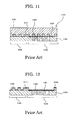
- a magnetic medium is produced using a metal mold 110 ( FIG.10 ) having a convex portion 101 in an area 100 corresponding to a data area (122 in FIG.11 described later) and a large flat convex portion 104 in which a magnetic layer 103 is embedded in an area 102 corresponding to a servo area (123 in FIG.11 described later).
- the shapes of one of the data areas 122 and one of the servo areas 123 are processed by a metal film coating process ( FIG. 12 ) for coating with a metal film 130, a liftoff process ( FIG. 13 ), and an etching step carried out after removal of a resist residue 121 and the metal film 130 formed on the data area 122 and the servo area 123.
- the cross-section of a pattern composed of the servo areas 123 is larger than the cross-section of a pattern composed of the data areas 122, and a larger amount of the resist residue 121 remains in the servo areas than in the data areas.
- parts of the metal film on the servo area 123, which must remain after the liftoff process, are removed ( FIG.13 ).
- objects of the present invention are to provide a method for producing a magnetic recording medium that can stably produce next-generation magnetic recording media that have excellent signal integrity of servo areas, and to provide a magnetic recording medium produced by the production method, and a mold structure used in the production method.
- the present invention it is possible to solve the prior art problems, to achieve the aforementioned objects, and to provide a method for stably producing a next-generation magnetic recording medium that has excellent signal integrity of servo areas, a magnetic recording medium produced by the production method, and a mold structure used in the production method.
- the method for producing a magnetic recording medium according to the present invention includes at least an imprint resist forming step, a convexo-concave resist pattern forming step and a magnetism transfer step, and further includes other steps such as a resist applying step, a magnetic layer patterning step, and a resist removing step as required.
- the magnetic recording medium according to the present invention is produced by the method for producing a magnetic recording medium according to the present invention.
- the magnetic recording medium according to the present invention will also be described in detail through the description of the method for producing a magnetic recording medium according to the present invention.
- the imprint resist forming step is a step in which as shown in FIG.1 , an imprint resist layer 13 is formed on a surface of a magnetic recording medium base 12 having a magnetic layer 11 on a surface (preferably on both sides of a substrate) of a substrate 10.
- the shape, structure, size and material of the substrate 10 are not particularly limited and can be appropriately selected depending on the purpose; for example, when the magnetic recording medium is a magnetic disc in a hard disc and the like, it has a disc-shape.
- the structure of the substrate may be a single-layer structure or laminated structure.
- the material of the substrate may be appropriately selected from those known as substrate materials for magnetic recording media, and examples thereof include aluminum, glass, silicon, quartz and SiO 2 /Si in which a thermally-oxidized film is formed on a silicon surface. These materials for substrate may be used alone or in combination of two or more.
- a material used for the magnetic layer 11 is not particularly limited, can be appropriately selected from those known in the art depending on the purpose, and preferred examples thereof include, Fe, Co, Ni, FeCo, FeNi, CoNi, CoNiP, FePt, CoPt and NiPt. These may be used alone or in combination of two or more.
- the thickness of the magnetic layer 11 is not particularly limited, can be appropriately selected depending on the purpose, and is usually about 5 nm to 30 nm.
- the method for forming the magnetic layer 11 is not particularly limited, the magnetic layer 11 can be formed by a known method, and examples of the method include sputtering method and electrodeposition (method).
- a crystal orientation layer for orienting the magnetic layer and a soft magnetic undercoat layer may be formed as required between the substrate 10 and the magnetic layer 11.
- the soft magnetic undercoat layer may be a single layer or laminate layer.
- the imprint resist layer 13 is not particularly limited, can be appropriately selected from those known in the art depending on the purpose, and is, for example, a layer formed by coating a surface of the magnetic recording medium base 12 with an imprint resist composition (hereinafter it is sometimes referred to as "imprint resist solution”) containing at least any one of a thermosetting resin and a photocurable resin.
- imprint resist solution an imprint resist composition
- materials of the imprint resist composition used for forming the imprint resist layer 13 materials that do not inhibit transfer of magnetic signals, in the magnetism transfer step, from a mold structure 1 shown in FIG.2 described later to the magnetic recording medium base 12, that is, materials having a relative magnetic permeability of 1 or more are used, examples of such materials include novolac resins, epoxy resins, acrylic resins, organic glass resins, and inorganic glass resins.
- fine metal particles may be dispersed in the resist in order to increase the relative magnetic permeability.
- the fine metal particles are fine particles of a metal containing at least one selected from Fe, Co and Ni, or an alloy thereof.
- such a non-magnetic element as Pt, In, Ru, O and N may be introduced to the imprint resist composition.
- thermal NIL thermal NIL
- photo-NIL photo-NIL
- thermal NIL The following is a description of the thermal NIL.
- a convexo-concave pattern is formed by pressing a plurality of convex portions 3 of a mold structure 1 against an imprint resist layer 13 formed on a surface of a magnetic recording medium base 12.
- the temperature of the system is kept near the glass transition temperature (Tg) of the imprint resist solution, after the transfer of the pattern to the surface of the imprint resist layer, the temperature of the resist layer is controlled to be lower than the glass transition temperature (Tg) of the resist solution to cure the imprint resist layer.
- Tg glass transition temperature
- Tg glass transition temperature
- a convexo-concave resist pattern is formed using a mold structure 1 composed of a material which has optical transparency and a strength to serve as a mold structure (for example, quartz (SiO 2 ) and organic resins (PET, PEN, polycarbonate, and fluorine resins having a low-melting point)).
- a mold structure 1 composed of a material which has optical transparency and a strength to serve as a mold structure (for example, quartz (SiO 2 ) and organic resins (PET, PEN, polycarbonate, and fluorine resins having a low-melting point)).
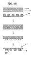
- a material has optical transparency specifically means that as shown in FIG. 4B described later, when a light beam is incident from a certain surface of the master base 53 to be processed such that the light beam exits from at least the other surface of the master base 53 to be processed on which the imprint resist layer 54 has been formed, the imprint resist solution is sufficiently cured, and means that the light transmittance of light beam having a wavelength of 400 nm or less emitted from the certain surface to the other surface of the substrate is 50% or more.
- the imprint resist layer 13 is irradiated with an ultraviolet ray to cure the transferred pattern.
- the pattern may be cured by exposing the imprint resist layer with ultraviolet ray even after the mold structure 1 is peeled off from the magnetic recording medium base 12 after patterning.
- the mold structure 1 is not particularly limited, can be appropriately selected from those known in the art depending on the purpose, and is, for example, as shown in FIG. 3 , provided with a plurality of convex portions 3 formed at a predetermined interval and further provided with other convexo-concave portions as required on one surface 2a (hereinafter, may be referred to as "reference surface 2a") of a disc-shaped master base 2.
- reference surface 2a one surface 2a
- the mold structure 1 needs to be composed of a ferromagnetic material at least in the vicinity of the outermost surfaces of convex portion so that magnetism can be transferred.
- the ferromagnetic material is composed of a metal or an alloy containing at least one selected from Fe, Co, Ni, Cr, Ta, W, Pt, Ru, O and the like.
- the master base itself having a convexo-concave pattern may be composed of a ferromagnetic material.
- an undercoat layer may be provided in order to control magnetic anisotropy of the magnetic layer.
- a protective layer may be provided on the surface of the mold structure 1. This protective layer is preferably, for example, composed of a hard carbon material and has a thickness of about 2 nm to 10 nm.
- convex portions 3 include data-pattern convex portions 3a corresponding to a data area 12a ( FIG. 2 ) and servo-pattern convex portions 3b corresponding to a servo area 12b ( FIG. 2 ).
- An area difference of convex portions between each of the data areas and each of the servo areas can be kept small by providing a convexo-concave pattern corresponding to servo signals in the servo-pattern convex portions 3b, in addition to the convexo-concave pattern provided in the data-pattern convex portions 3a.
- the amount of resist residue 13a remaining between the mold structure 1 and the magnetic recording medium base 12 in nanoimprint lithography (NIL), especially the amount of resist residue in the servo area 123 can be reduced and a state where the resist residue remains almost even can be realized throughout the entire surface of the magnetic recording medium base 12.
- the other members are not particularly limited, can be appropriately selected depending on the purpose, as long as the use of them does not impair the effects of the present invention, and for example, a mold surface layer formed on a master base 2 and having a function of peeling off from an imprint resist layer 13 is exemplified.
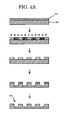
- FIGS. 4A and 4B are cross-sectional views exemplarily showing a method for producing a mold structure 1.
- a photoresist solution such as a novolac resin and an acrylic resin is applied onto an Si base 50 by spin coating or the like to form a photoresist layer 51.
- the Si base 50 is irradiated with a laser beam (or an electron beam) that is modulated according to a servo signal with rotating the Si base 50 to expose a predetermined pattern at a corresponding part of each frame on tracks over the entire photoresist surface.
- the predetermined pattern is, for example, a pattern corresponding to a servo signal that extends linearly in a radial direction from the rotational center.
- the photoresist layer 51 is developed to remove those portions exposed, the pattern of the photoresist layer 51 from which those portions have been removed is used as a mask and the Si base 50 is selectively etched by RIE to thereby obtain an original master 52 having convexo-concave patterns.
- a plating method, a nanoimprint method and the like may be used.
- the method for producing the mold structure 1 by plating method is described below.
- a conductive layer (not shown) is formed on a surface of the original master 52.
- a vacuum film-forming method such as sputtering and vapor deposition), a nonelectrolytic plating method and the like may be generally used.
- a material used for the conductive layer a metal or an alloy containing at least one selected from Ni, Cr, W, Ta, Fe and Co may be used. Ni, Co and an alloy of FeCo are desirable.
- a nonmetal material having conductive property, such as TiO, may also be used as a conductive layer.
- the thickness of the conductive layer is in the range of 5 nm to 30 nm. The range of 10 nm to 25 nm is more desirable.
- a metal material or an alloy material is deposited by plating method until a plated base has a predetermined thickness, and then the plated base is peeled off from the original master 52, thereby forming the mold structure 1.
- the plating material used for the mold structure Ni, Cr, an alloy of FeCo and the like may be used, and an Ni material is preferably used.
- the thickness of the mold structure after the plated base being peeled off is in the range of 30 ⁇ m to 500 ⁇ m, and preferably in the range of 45 ⁇ m to 300 ⁇ m. When the thickness is 30 ⁇ m or less, the rigidity of the mold structure 1 is reduced, and sufficient mechanical property cannot be secured.
- the mold structure 1 itself deform, resulting in a significant degradation of properties in practical use.
- the thickness is 500 ⁇ m or more
- the rigidity of the mold structure 1 becomes too high to secure tight adhesion between the mold structure 1 and the magnetic recording medium at the time of transfer of magnetism in NIL.
- an adhesion pressure therebetween needs to be increased, and thus a fatal pattern defect may occur in the mold structure 1 and/or the magnetic recording medium when a foreign object is incorporated thereinto.
- the mold structure 1 may be reproduced using the above mentioned mold as the original master 52.
- an imprint resist solution containing a thermoplastic resin or a photocurable resin is applied onto one surface of a master base to be processed 53 to form an imprint resist layer 54, and then the original master 52 is pressed against the imprint resist layer 54 to transfer the convex portion pattern formed in the surface of the original master 52 to the imprint resist layer 54.
- a material used for the master base 53 to be processed is not particularly limited, can be appropriately selected depending on the purpose, as long as it has optical transparency and has a strength to serve as a mold structure 1, and examples thereof include quartz (SiO 2 ) and organic resins (PET, PEN, polycarbonate and fluorine resins having a low-melting point).
- a material has optical transparency specifically means that when a light beam is incident from a certain surface of the master base 53 to be processed such that the light beam exits from the other surface on which the imprint resist layer 54 has been formed, the imprint resist solution is sufficiently cured, and means that the light transmittance of light beam having a wavelength of 400 nm or less emitted from the certain surface to the other surface of the master base 53 to be processed is 50% or more.
- the transferred pattern is cured by applying heat or ultraviolet ray to the imprint resist layer 54.
- the pattern is cured by exposure to an ultraviolet ray, it may be exposed to ultraviolet ray and cured after the mold structure is peeled off from the magnetic recording medium after patterning.
- the master base was selectively etched by RIE or the like while using the transferred pattern as a mask, thereby obtaining a mold structure 1 having a convexo-concave pattern. Furthermore, an inorganic material may be formed on the surface of the master base to form a mask of the inorganic material based on the resist mask, and the master base may be etched using this inorganic material mask to form the mold structure 1.
- a magnetic layer for magnetism transfer is formed.
- a vacuum film-forming method sputtering, vapor deposition and the like
- a plating method and the like may be used.
- a material used for the magnetism-transfer magnetic layer a metal or an alloy containing at least one selected from Fe, Co, Ni, Cr, Pt, B, W and Ta may be used. FeCo alloys, FeCoNi alloys and the like having high saturation magnetization are desirable.
- the thickness of the magnetic layer is in the range of 10 nm to 200 nm.
- the range of 50 nm to 150 nm is more desirable.
- the mold structure 1 may be formed using a material used for the magnetism transfer magnetic layer.
- an initialization magnetic field is previously applied to the magnetic recording medium base 12 (slave disc) such that a magnetic flux is applied in a perpendicular direction to the surface of the substrate 10 and the surface of the substrate is uniformly magnetized in one direction.
- a predetermined magnetic field 60 is applied to the initialized magnetic recording medium base 12 (slave disc) in the reverse direction to the initialization magnetic field via the mold structure 1 ( FIG.5 ), and magnetism is transferred to the magnetic layer 11 corresponding to the servo area 12b and the data area 12a so that magnetization 61 orients in a positive direction and magnetization 62 in a negative direction.
- the predetermined magnetic field 60 is composed of a transfer magnetic field in the opposite direction to the initialization magnetic field.
- the predetermined magnetic field 60 is applied to the imprint mold structure 1, which leads the magnetic flux in the direction perpendicular to the surface of the substrate 10, and a magnetization of the magnetic layer is established thereby.
- the resist coating step is a step, as shown in FIG.7 , of coating an area of a convexo-concave resist pattern formed in an imprint resist layer 13 corresponding to a servo area 12b with a resist layer 70 (second resist layer).
- a peel coat method, a photolithographic method using a mask and an ink-jet method may be used.
- At least one selected from novolac resins, epoxy resins, acrylic resins, organic glass resins, inorganic resins and the like may be preferably used, similarly to the material used for the imprint resist composition.
- a material insoluble in a solvent used in the imprint resist may be used.
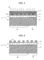
- the magnetic layer patterning step is a step, as shown in FIG.8 , of forming a convexo-concave pattern on a magnetic layer 11 corresponding to a data area 12a based on a convexo-concave resist pattern formed in the imprint resist layer 13 corresponding to the data area 12a, using as a mask the resist layer 70 corresponding to a servo area 12b.
- a method for forming the convexo-concave pattern such a technique as ion beam etching, RIE or wet etching may be used.
- Ar gas may be used as a process gas for ion beam etching, and CO plus NH 3 , a chlorine gas and the like may be used as an etchant for RIE.
- magnetism transferred to the data area 12a disappears or attenuates.
- the resist removing step is a step, as shown in FIG.9 , of removing the imprint resist layer 13 on convex portions 11a of the magnetic layer 11.
- a permeation method using a solvent capable of dissolving a resist, a reactive ion etching method or the like may be used.
- an ultrasonic wave may be applied to the imprint resist layer 13 to accelerate the removal of the resist.
- a step of embedding nonmagnetic material such as SiO 2 , carbon, alumina, polymer such as polymethylmethacrylate (PMMA) or polystyrene (PS), or a lubricant oil in concave portions 11b of the magnetic layer, a step of smoothing the surface of the magnetic layer, a step of forming a protective layer on the smoothed surface with DLC (diamond-like carbon) or the like, and a final step of applying a lubricant oil are exemplified.
- the magnetic recording medium according to the present invention is produced by the method for producing a magnetic recording medium described above, and, as shown in FIG.9 , servo signals in the servo area 12b are formed of magnetization 61 that is oriented in a positive direction and magnetization 62 that is oriented in a negative direction.
- the dimensional tolerance of a convexo-concave pattern formed in the data area 12a is 15 nm (3 ⁇ ) or less. Note that "3 ⁇ " means a value of 3 ⁇ of the width of convex portions of the magnetic layer constituting the data area 12a.
- the magnetic recording medium produced by the method for producing the magnetic recording medium of the present invention is preferably at least any one of a discrete magnetic recording medium and a patterned magnetic recording medium.
- An electron beam resist was applied onto an 8-inch Si wafer by spin coating to form a layer of 100 nm in thickness.
- a desired pattern of the electron beam resist was exposed and developed using a rotary electron beam exposing device to produce a resist Si base having a convexo-concave pattern.
- the resist Si base having the convexo-concave pattern was subjected to a reactive ion etching treatment using the convexo-concave resist as a mask to form the convexo-concave pattern on the Si base.
- a remaining resist was removed by washing with a solvent capable of dissolving the resist, and the Si base was dried to thereby obtain an original master.
- the pattern used was broadly classified into data areas and servo areas.
- Each of servo areas had a basic signal length of 80 nm, the total number of sectors was 120, and each of the servo areas was composed of a preamble area (40 bit), a servo mark area (6 bit), a Sector Code area (8 bit), a Cylinder Code area (32 bit) and a burst area (Burst pattern).
- the servo mark identification code is "001010", and for Sector Code areas, a binary conversion method is used, and for Cylinder Code areas, a gray conversion method is used. For burst areas, commonly used 4 bursts (each burst is 16 bit) and Manchester conversion method are employed.
- an Ni conductive film of 20 nm in thickness was formed by sputtering.
- the original master coated with the conductive film was soaked in a nickel sulfamate bath to form an Ni film of 200 ⁇ m in thickness by electrolytic plating, and the Ni film was peeled off from the Si original master and washed to obtain a mold intermediate member by plating.
- An FeCo30 atom% magnetic layer of 100 nm in thickness was formed on a surface of the mold intermediate member by sputtering to obtain a mold.
- a perpendicular magnetic recording medium was produced on a 2.5 inch glass substrate according to the following method.
- the produced perpendicular magnetic recording medium was provided with at least, a soft magnetic layer, a first nonmagnetic orientation layer, a second nonmagnetic orientation layer, a magnetic recording layer (magnetic layer), a protective layer and a lubricant layer formed in this order.
- the soft magnetic layer, the first nonmagnetic orientation layer, the second nonmagnetic orientation layer, the magnetic recording layer and the protective layer were prepared by sputtering, and the lubricant layer was prepared by dipping method.
- CoZrNb was laminated to form a layer of 100 nm in thickness. Specifically, the glass substrate was set so as to face the CoZrNb target, then an Ar gas was injected such that the pressure was 0.6 Pa, and the soft magnetic layer was formed at 1,500 W (DC).
- the first nonmagnetic orientation layer Ti was sputtered to form a layer of 5 nm in thickness, and for the second nonmagnetic orientation layer, Ru was sputtered to form a layer of 10 nm in thickness.
- the first nonmagnetic orientation layer was set so as to face the Ti target, then an Ar gas was injected such that the pressure was 0.5 Pa, and the Ti seed layer was formed with a DC discharge (1,000 W) so as to have a thickness of 5 nm.
- the first nonmagnetic orientation layer formed over the substrate was set so as to face the Ru target, then an Ar gas was injected such that the pressure was 0.5 Pa, and the second nonmagnetic orientation layer composed of Ru was formed with a DC discharge (1,000 W) so as to have a thickness of 10 nm.
- CoCrPtO was sputtered to form a layer of 15 nm in thickness.
- the second nonmagnetic orientation layer formed over the substrate was set so as to face the CoPtCr target, then an Ar gas containing O 2 at 0.04% was injected such that the pressure was 18 Pa, and the recording layer was formed with a DC discharge (290 W).
- the magnetic layer formed over the substrate was set so as to face the C target, then an Ar gas was injected such that the pressure was 0.5 Pa, and a C protective layer of 4 nm in thickness was formed with a DC discharge (1,000 W).
- the coercive force of the perpendicular magnetic recording medium was 334 kA/m (4.2 kOe).
- the perpendicular magnetic recording medium was initialized.
- a novolac resist (Microresist company; mr-I7000E) was applied over the surface of the perpendicular magnetic recording medium by spin coating at 3,600 rpm so as to have a thickness of 100 nm.
- the mold was set so as to face the perpendicular magnetic recording medium that had been coated with the resist, the perpendicular magnetic recording medium was heated at 100°C, then the mold was pressed against the perpendicular magnetic recording medium at a pressure of 3 MPa for 10 sec for adhesion, and a magnetic field was applied to carry out magnetism transfer.
- the magnetic intensity used for the magnetism transfer was 4.2 kOe. After the magnetic field was applied, the mold was peeled off from the perpendicular magnetic recording medium.
- resist layer 70 in FIG.7 was bonded to servo areas with a peel coat.
- the magnetic layer was processed to form a convexo-concave pattern.
- an ion beam etching method was employed using an Ar gas.
- the remaining resist layer was removed with O 2 RIE, and a PFPE lubricant was applied to form a layer of 2 nm in thickness by dipping method.
- a magnetic recording medium of Example 2 was produced in the same manner as in Example 1, except that fine Co particles (diameter: 10 nm) were dispersed in the novolac resist to obtain an imprint resist layer having a relative magnetic permeability of 2.1.
- a magnetic recording medium of Example 3 was produced in the same manner as in Example 1, except that fine Ag particles (diameter: 15 nm) were dispersed in the novolac resist to obtain an imprint resist layer having a relative magnetic permeability of 0.98.
- a magnetic recording medium of Example 4 was produced in the same manner as in Example 1, except that fine Ag particles (diameter: 50 nm) were dispersed in the novolac resist to obtain an imprint resist layer having a relative magnetic permeability of 0.9.
- a magnetic recording medium of Comparative Example 1 was produced in the same manner as in Example 1, except that the convexo-concave pattern corresponding to servo areas was not formed on the imprint resist layer to prepare a mold structure in which the corresponding portions were made flat (as in a method according to JP-A No.2006-216200 ).
- the resist patterns were compared between data areas and servo areas, and NIL uniformity was evaluated as follows.
- each of the intermediate members of the intermediate perpendicular magnetic recording media were fractured, and then the film thickness of a resist residue remaining in the data areas and the film thickness of a resist residue remaining in a burst area in the servo areas were measured (using a scanning electron microscope, FE-SEM S800 manufactured by Hitachi, Ltd.).
- the ratio of the film thickness of the resist residue remaining in the data areas to the film thickness of the resist residue remaining in the burst area in the servo areas was in the range of 0.8 to 1.0, the formability of resist pattern was evaluated as "A"; when the ratio was less than 0.8, and the resist pattern formability was evaluated as "C".
- the thicknesses of the resist samples were measured at eight sites per disc within an area having a radius of 25 mm at generally equiangular spacing, and the average of the eight ratios was calculated to thereby evaluate the resist pattern formability. The results are shown in Table 1.
- reproduction output powers of TAA Track Average Amplitude
- LS-90 manufactured by Kyodo Denshi, K.K.
- Uniformity of the widths of convex portions in each of the magnetic layers was evaluated for the pattern corresponding to data areas using an AFM (Dimension 5000, manufactured by Veeco Instruments). The evaluation was carried out within a range of 1 ⁇ m square to retrieve data on the convexo-concave pattern on each of the surfaces of the magnetic layers.
- a threshold was set at 80% of the height of the pattern composed of convex portions on each of the processed magnetic layers, and dimensional variations in the side surface area of a convex portion formed when the convex portion was sliced with the threshold were evaluated using a standard deviation (in visual field of 1 ⁇ m square).
Landscapes
- Engineering & Computer Science (AREA)
- Chemical & Material Sciences (AREA)
- Nanotechnology (AREA)
- Physics & Mathematics (AREA)
- Mathematical Physics (AREA)
- Theoretical Computer Science (AREA)
- Crystallography & Structural Chemistry (AREA)
- Manufacturing Of Magnetic Record Carriers (AREA)
- Magnetic Record Carriers (AREA)
Applications Claiming Priority (1)
| Application Number | Priority Date | Filing Date | Title |
|---|---|---|---|
| JP2007162771A JP4742073B2 (ja) | 2007-06-20 | 2007-06-20 | 磁気記録媒体の製造方法 |
Publications (1)
| Publication Number | Publication Date |
|---|---|
| EP2006842A1 true EP2006842A1 (de) | 2008-12-24 |
Family
ID=39642629
Family Applications (1)
| Application Number | Title | Priority Date | Filing Date |
|---|---|---|---|
| EP08011284A Withdrawn EP2006842A1 (de) | 2007-06-20 | 2008-06-20 | Verfahren zur Herstellung eines magnetischen Aufzeichnungsmediums, damit hergestelltes magnetisches Aufzeichnungsmedium und Formstruktur zur Verwendung für dieses Verfahren |
Country Status (3)
| Country | Link |
|---|---|
| US (1) | US20080316649A1 (de) |
| EP (1) | EP2006842A1 (de) |
| JP (1) | JP4742073B2 (de) |
Families Citing this family (4)
| Publication number | Priority date | Publication date | Assignee | Title |
|---|---|---|---|---|
| JP4742074B2 (ja) * | 2007-06-29 | 2011-08-10 | 富士フイルム株式会社 | 磁気記録媒体の製造方法 |
| JP5037243B2 (ja) * | 2007-07-06 | 2012-09-26 | 富士フイルム株式会社 | 界面結合剤、該界面結合剤を含有するレジスト組成物、及び該界面結合剤からなる層を有する磁気記録媒体形成用積層体、並びに該界面結合剤を用いた磁気記録媒体の製造方法、及び該製造方法により製造された磁気記録媒体 |
| JP2009043317A (ja) * | 2007-08-07 | 2009-02-26 | Fujifilm Corp | 磁気記録媒体の製造装置及び磁気記録媒体の製造方法 |
| US8685547B2 (en) * | 2009-02-19 | 2014-04-01 | Seagate Technology Llc | Magnetic recording media with enhanced writability and thermal stability |
Citations (5)
| Publication number | Priority date | Publication date | Assignee | Title |
|---|---|---|---|---|
| US5991104A (en) * | 1996-11-27 | 1999-11-23 | Seagate Technology, Inc. | Using servowriter medium for quickly written servo-patterns on magnetic media |
| US6086961A (en) * | 1998-03-09 | 2000-07-11 | Seagate Technology, Inc. | Quickly written servo-patterns for magnetic media including removing |
| US20050094298A1 (en) * | 2003-09-22 | 2005-05-05 | Kabushiki Kaisha Toshiba | Imprint stamper, method for manufacturing the same, recording medium, method for manufacturing the same, information recording/reproducing method, and information recording/reproducing apparatus |
| EP1688926A1 (de) * | 2005-02-07 | 2006-08-09 | Fujitsu Limited | Verfahren zur Herstellung magnetischer Aufzeichnungsmittel und Rakel dafür |
| WO2007010457A2 (en) * | 2005-07-21 | 2007-01-25 | Nxp B.V. | Magnetic rom information carrier |
-
2007
- 2007-06-20 JP JP2007162771A patent/JP4742073B2/ja not_active Expired - Fee Related
-
2008
- 2008-06-19 US US12/142,611 patent/US20080316649A1/en not_active Abandoned
- 2008-06-20 EP EP08011284A patent/EP2006842A1/de not_active Withdrawn
Patent Citations (6)
| Publication number | Priority date | Publication date | Assignee | Title |
|---|---|---|---|---|
| US5991104A (en) * | 1996-11-27 | 1999-11-23 | Seagate Technology, Inc. | Using servowriter medium for quickly written servo-patterns on magnetic media |
| US6086961A (en) * | 1998-03-09 | 2000-07-11 | Seagate Technology, Inc. | Quickly written servo-patterns for magnetic media including removing |
| US20050094298A1 (en) * | 2003-09-22 | 2005-05-05 | Kabushiki Kaisha Toshiba | Imprint stamper, method for manufacturing the same, recording medium, method for manufacturing the same, information recording/reproducing method, and information recording/reproducing apparatus |
| EP1688926A1 (de) * | 2005-02-07 | 2006-08-09 | Fujitsu Limited | Verfahren zur Herstellung magnetischer Aufzeichnungsmittel und Rakel dafür |
| JP2006216200A (ja) | 2005-02-07 | 2006-08-17 | Fujitsu Ltd | 磁気媒体の製造方法および磁気媒体製造用金型 |
| WO2007010457A2 (en) * | 2005-07-21 | 2007-01-25 | Nxp B.V. | Magnetic rom information carrier |
Also Published As
| Publication number | Publication date |
|---|---|
| JP4742073B2 (ja) | 2011-08-10 |
| US20080316649A1 (en) | 2008-12-25 |
| JP2009004012A (ja) | 2009-01-08 |
Similar Documents
| Publication | Publication Date | Title |
|---|---|---|
| JP5053007B2 (ja) | インプリント用モールド構造体、及び該インプリント用モールド構造体を用いたインプリント方法、並びに、磁気記録媒体 | |
| US20090029189A1 (en) | Imprint mold structure, and imprinting method using the same, as well as magnetic recording medium, and method for manufacturing magnetic recording medium | |
| EP1256940A2 (de) | Urträger für magnetische Übertragung | |
| CN100446089C (zh) | 被构图基底,制造基底的方法,磁记录介质及磁记录装置 | |
| EP2026338A1 (de) | Vorrichtung und Verfahren zur Herstellung eines magnetischen Aufzeichnungsmediums | |
| US20080241601A1 (en) | Mold structure, imprinting method using the same, magnetic recording medium and production method thereof | |
| US20080316649A1 (en) | Method for producing magnetic recording medium, magnetic recording medium produced by the production method, and mold structure for use in the production method | |
| JP5033003B2 (ja) | モールド構造体及びそれを用いたインプリント方法、並びに磁気記録媒体及びその製造方法 | |
| US20080248334A1 (en) | Mold structure, imprinting method using the same, magnetic recording medium and production method thereof | |
| JP2008276907A (ja) | モールド構造体、及びそれを用いたインプリント方法、並びに磁気記録媒体及びその製造方法 | |
| JP2009070544A (ja) | 磁気記録媒体の製造方法、及び磁気記録媒体 | |
| JP2010102820A (ja) | モールド構造体、並びにそれを用いたインプリント方法及び磁気転写方法 | |
| EP2009624A1 (de) | Verfahren zur Herstellung eines magnetischen Aufzeichnungsmediums, magnetisches Aufzeichnungsmedium, das mit dem Herstellungsverfahren hergestellt wurde, und Formstruktur zur Verwendung im Herstellungsverfahren | |
| EP2107559A1 (de) | Verfahren zur Herstellung von Trägermatrizen für magnetische Übertragung, magnetische Übertragungssträgermatrizen, magnetisches Übertragungsverfahren und magnetisches Aufzeichnungsmedium | |
| JP2009208447A (ja) | インプリント用モールド構造体、並びにインプリント方法、磁気記録媒体及びその製造方法 | |
| US20080248333A1 (en) | Mold structure, imprinting method using the same, magnetic recording medium and production method thereof | |
| US20090147405A1 (en) | Method for manufacturing magnetic recording medium, magnetic recording medium manufactured by the same, and magnetic recording apparatus incorporating the magnetic recording medium | |
| JP2008276906A (ja) | モールド構造体、及びそれを用いたインプリント方法、並びに磁気記録媒体及びその製造方法 | |
| US6979524B2 (en) | Contact printing of longitudinal magnetic media with perpendicularly applied magnetic field | |
| KR20020069135A (ko) | 자기전사방법 및 자기전사장치 | |
| JP2009004066A (ja) | モールド構造体及びそれを用いたインプリント方法、並びに磁気記録媒体及びその製造方法 | |
| JP4761166B2 (ja) | 磁気転写用マスター体の製造方法 | |
| JP2009048752A (ja) | インプリント用モールド構造体、及び該インプリント用モールド構造体を用いたインプリント方法、並びに、磁気記録媒体、及びその製造方法 | |
| KR20090104720A (ko) | 자기 전사용 마스터 담체의 제조 방법, 자기 전사용 마스터담체, 자기 전사 방법, 및 자기 기록 매체 | |
| JP2009043316A (ja) | インプリント用モールド構造体、及び該モールド構造体を用いたインプリント方法、並びに磁気記録媒体、及びその製造方法 |
Legal Events
| Date | Code | Title | Description |
|---|---|---|---|
| PUAI | Public reference made under article 153(3) epc to a published international application that has entered the european phase |
Free format text: ORIGINAL CODE: 0009012 |
|
| AK | Designated contracting states |
Kind code of ref document: A1 Designated state(s): AT BE BG CH CY CZ DE DK EE ES FI FR GB GR HR HU IE IS IT LI LT LU LV MC MT NL NO PL PT RO SE SI SK TR |
|
| AX | Request for extension of the european patent |
Extension state: AL BA MK RS |
|
| 17P | Request for examination filed |
Effective date: 20090605 |
|
| 17Q | First examination report despatched |
Effective date: 20090723 |
|
| AKX | Designation fees paid |
Designated state(s): DE FR GB |
|
| STAA | Information on the status of an ep patent application or granted ep patent |
Free format text: STATUS: THE APPLICATION IS DEEMED TO BE WITHDRAWN |
|
| 18D | Application deemed to be withdrawn |
Effective date: 20100415 |