EP2006875B1 - Elektronenemissionselement, anzeige mit dem elektronenemissionselement und verfahren zur herstellung des elektronenemissionselements - Google Patents
Elektronenemissionselement, anzeige mit dem elektronenemissionselement und verfahren zur herstellung des elektronenemissionselements Download PDFInfo
- Publication number
- EP2006875B1 EP2006875B1 EP07739652A EP07739652A EP2006875B1 EP 2006875 B1 EP2006875 B1 EP 2006875B1 EP 07739652 A EP07739652 A EP 07739652A EP 07739652 A EP07739652 A EP 07739652A EP 2006875 B1 EP2006875 B1 EP 2006875B1
- Authority
- EP
- European Patent Office
- Prior art keywords
- layer
- electron supply
- electron
- supply layer
- emitting device
- Prior art date
- Legal status (The legal status is an assumption and is not a legal conclusion. Google has not performed a legal analysis and makes no representation as to the accuracy of the status listed.)
- Ceased
Links
- 238000004519 manufacturing process Methods 0.000 title claims description 33
- OKTJSMMVPCPJKN-UHFFFAOYSA-N Carbon Chemical compound [C] OKTJSMMVPCPJKN-UHFFFAOYSA-N 0.000 claims abstract description 130
- 229910052799 carbon Inorganic materials 0.000 claims abstract description 129
- 230000005684 electric field Effects 0.000 claims abstract description 9
- 239000013078 crystal Substances 0.000 claims description 80
- KFYRPLNVJVHZGT-UHFFFAOYSA-N Amitriptyline hydrochloride Chemical compound Cl.C1CC2=CC=CC=C2C(=CCCN(C)C)C2=CC=CC=C21 KFYRPLNVJVHZGT-UHFFFAOYSA-N 0.000 claims description 14
- 239000002245 particle Substances 0.000 claims description 11
- 238000004140 cleaning Methods 0.000 claims description 10
- 238000010438 heat treatment Methods 0.000 claims description 5
- 238000000034 method Methods 0.000 claims description 5
- 238000005530 etching Methods 0.000 claims description 2
- 239000012212 insulator Substances 0.000 abstract description 6
- -1 Ge-Si Chemical compound 0.000 description 19
- 238000004544 sputter deposition Methods 0.000 description 14
- 239000000463 material Substances 0.000 description 13
- 238000010586 diagram Methods 0.000 description 12
- 239000000758 substrate Substances 0.000 description 12
- 230000015572 biosynthetic process Effects 0.000 description 11
- 238000002425 crystallisation Methods 0.000 description 9
- 230000008025 crystallization Effects 0.000 description 9
- 229910052751 metal Inorganic materials 0.000 description 9
- 239000002184 metal Substances 0.000 description 9
- 230000004888 barrier function Effects 0.000 description 8
- 230000000052 comparative effect Effects 0.000 description 8
- 239000004065 semiconductor Substances 0.000 description 8
- 230000008859 change Effects 0.000 description 7
- 230000004048 modification Effects 0.000 description 6
- 238000012986 modification Methods 0.000 description 6
- VYPSYNLAJGMNEJ-UHFFFAOYSA-N Silicium dioxide Chemical compound O=[Si]=O VYPSYNLAJGMNEJ-UHFFFAOYSA-N 0.000 description 5
- 229910021417 amorphous silicon Inorganic materials 0.000 description 5
- 230000007547 defect Effects 0.000 description 5
- 229910052710 silicon Inorganic materials 0.000 description 5
- 229910052814 silicon oxide Inorganic materials 0.000 description 5
- BOTDANWDWHJENH-UHFFFAOYSA-N Tetraethyl orthosilicate Chemical compound CCO[Si](OCC)(OCC)OCC BOTDANWDWHJENH-UHFFFAOYSA-N 0.000 description 4
- NRTOMJZYCJJWKI-UHFFFAOYSA-N Titanium nitride Chemical compound [Ti]#N NRTOMJZYCJJWKI-UHFFFAOYSA-N 0.000 description 4
- 229910052782 aluminium Inorganic materials 0.000 description 4
- 238000005229 chemical vapour deposition Methods 0.000 description 4
- PXHVJJICTQNCMI-UHFFFAOYSA-N nickel Substances [Ni] PXHVJJICTQNCMI-UHFFFAOYSA-N 0.000 description 4
- 238000005268 plasma chemical vapour deposition Methods 0.000 description 4
- HBMJWWWQQXIZIP-UHFFFAOYSA-N silicon carbide Chemical compound [Si+]#[C-] HBMJWWWQQXIZIP-UHFFFAOYSA-N 0.000 description 4
- XMWRBQBLMFGWIX-UHFFFAOYSA-N C60 fullerene Chemical compound C12=C3C(C4=C56)=C7C8=C5C5=C9C%10=C6C6=C4C1=C1C4=C6C6=C%10C%10=C9C9=C%11C5=C8C5=C8C7=C3C3=C7C2=C1C1=C2C4=C6C4=C%10C6=C9C9=C%11C5=C5C8=C3C3=C7C1=C1C2=C4C6=C2C9=C5C3=C12 XMWRBQBLMFGWIX-UHFFFAOYSA-N 0.000 description 3
- 229910045601 alloy Inorganic materials 0.000 description 3
- 239000000956 alloy Substances 0.000 description 3
- 229910052796 boron Inorganic materials 0.000 description 3
- 229910052804 chromium Inorganic materials 0.000 description 3
- 239000011651 chromium Substances 0.000 description 3
- 238000000151 deposition Methods 0.000 description 3
- 230000008021 deposition Effects 0.000 description 3
- 229910003472 fullerene Inorganic materials 0.000 description 3
- 238000005259 measurement Methods 0.000 description 3
- 229910052750 molybdenum Inorganic materials 0.000 description 3
- 229910052759 nickel Inorganic materials 0.000 description 3
- 238000005289 physical deposition Methods 0.000 description 3
- 229910052697 platinum Inorganic materials 0.000 description 3
- 239000010703 silicon Substances 0.000 description 3
- 229910010271 silicon carbide Inorganic materials 0.000 description 3
- 229910052719 titanium Inorganic materials 0.000 description 3
- 239000010936 titanium Substances 0.000 description 3
- 229910052721 tungsten Inorganic materials 0.000 description 3
- CSCPPACGZOOCGX-UHFFFAOYSA-N Acetone Chemical compound CC(C)=O CSCPPACGZOOCGX-UHFFFAOYSA-N 0.000 description 2
- IJGRMHOSHXDMSA-UHFFFAOYSA-N Atomic nitrogen Chemical compound N#N IJGRMHOSHXDMSA-UHFFFAOYSA-N 0.000 description 2
- ZOXJGFHDIHLPTG-UHFFFAOYSA-N Boron Chemical compound [B] ZOXJGFHDIHLPTG-UHFFFAOYSA-N 0.000 description 2
- 229910052684 Cerium Inorganic materials 0.000 description 2
- VYZAMTAEIAYCRO-UHFFFAOYSA-N Chromium Chemical compound [Cr] VYZAMTAEIAYCRO-UHFFFAOYSA-N 0.000 description 2
- 229910052692 Dysprosium Inorganic materials 0.000 description 2
- 229910052691 Erbium Inorganic materials 0.000 description 2
- 229910052693 Europium Inorganic materials 0.000 description 2
- 229910052688 Gadolinium Inorganic materials 0.000 description 2
- 229910005831 GeO3 Inorganic materials 0.000 description 2
- 229910052689 Holmium Inorganic materials 0.000 description 2
- 229910052765 Lutetium Inorganic materials 0.000 description 2
- 229910026161 MgAl2O4 Inorganic materials 0.000 description 2
- 229910017676 MgTiO3 Inorganic materials 0.000 description 2
- 229910052779 Neodymium Inorganic materials 0.000 description 2
- 229910052777 Praseodymium Inorganic materials 0.000 description 2
- 229910052772 Samarium Inorganic materials 0.000 description 2
- XUIMIQQOPSSXEZ-UHFFFAOYSA-N Silicon Chemical compound [Si] XUIMIQQOPSSXEZ-UHFFFAOYSA-N 0.000 description 2
- 229910004273 TeO3 Inorganic materials 0.000 description 2
- 229910052771 Terbium Inorganic materials 0.000 description 2
- 229910052775 Thulium Inorganic materials 0.000 description 2
- 229910010252 TiO3 Inorganic materials 0.000 description 2
- 229910052769 Ytterbium Inorganic materials 0.000 description 2
- 229910052793 cadmium Inorganic materials 0.000 description 2
- 238000005234 chemical deposition Methods 0.000 description 2
- 150000001875 compounds Chemical class 0.000 description 2
- 229910052802 copper Inorganic materials 0.000 description 2
- 229910003460 diamond Inorganic materials 0.000 description 2
- 239000010432 diamond Substances 0.000 description 2
- 239000007789 gas Substances 0.000 description 2
- 229910052737 gold Inorganic materials 0.000 description 2
- 229910052738 indium Inorganic materials 0.000 description 2
- 238000009413 insulation Methods 0.000 description 2
- 229910052741 iridium Inorganic materials 0.000 description 2
- 229910052742 iron Inorganic materials 0.000 description 2
- 229910052746 lanthanum Inorganic materials 0.000 description 2
- 229910052745 lead Inorganic materials 0.000 description 2
- 229910052748 manganese Inorganic materials 0.000 description 2
- 230000000873 masking effect Effects 0.000 description 2
- 229910052758 niobium Inorganic materials 0.000 description 2
- 229910052757 nitrogen Inorganic materials 0.000 description 2
- 230000003647 oxidation Effects 0.000 description 2
- 238000007254 oxidation reaction Methods 0.000 description 2
- 229910052763 palladium Inorganic materials 0.000 description 2
- 238000001259 photo etching Methods 0.000 description 2
- 238000005240 physical vapour deposition Methods 0.000 description 2
- 229920001296 polysiloxane Polymers 0.000 description 2
- 230000002265 prevention Effects 0.000 description 2
- 230000008569 process Effects 0.000 description 2
- 229910052702 rhenium Inorganic materials 0.000 description 2
- 229910052703 rhodium Inorganic materials 0.000 description 2
- 229910052706 scandium Inorganic materials 0.000 description 2
- 229910052709 silver Inorganic materials 0.000 description 2
- 229910052596 spinel Inorganic materials 0.000 description 2
- 229910052715 tantalum Inorganic materials 0.000 description 2
- 229910052713 technetium Inorganic materials 0.000 description 2
- 229910052716 thallium Inorganic materials 0.000 description 2
- 229910052718 tin Inorganic materials 0.000 description 2
- 229910052725 zinc Inorganic materials 0.000 description 2
- 229910052726 zirconium Inorganic materials 0.000 description 2
- NNDLQUNWZOIESH-UHFFFAOYSA-N 8-hydroxy-7-[[7-[(8-hydroxy-5-sulfoquinoline-7-carbonyl)amino]-4-[3-[(8-hydroxy-5-sulfoquinoline-7-carbonyl)amino]propyl]heptyl]carbamoyl]quinoline-5-sulfonic acid Chemical compound C1=CC=NC2=C(O)C(C(=O)NCCCC(CCCNC(=O)C=3C(=C4N=CC=CC4=C(C=3)S(O)(=O)=O)O)CCCNC(=O)C3=C(C4=NC=CC=C4C(=C3)S(O)(=O)=O)O)=CC(S(O)(=O)=O)=C21 NNDLQUNWZOIESH-UHFFFAOYSA-N 0.000 description 1
- 229910017988 AgVO3 Inorganic materials 0.000 description 1
- 229910000505 Al2TiO5 Inorganic materials 0.000 description 1
- 229910016384 Al4C3 Inorganic materials 0.000 description 1
- 229910017107 AlOx Inorganic materials 0.000 description 1
- JBRZTFJDHDCESZ-UHFFFAOYSA-N AsGa Chemical compound [As]#[Ga] JBRZTFJDHDCESZ-UHFFFAOYSA-N 0.000 description 1
- 229910017257 AsOx Inorganic materials 0.000 description 1
- QYEXBYZXHDUPRC-UHFFFAOYSA-N B#[Ti]#B Chemical compound B#[Ti]#B QYEXBYZXHDUPRC-UHFFFAOYSA-N 0.000 description 1
- 229910052580 B4C Inorganic materials 0.000 description 1
- 229910016010 BaAl2 Inorganic materials 0.000 description 1
- 229910002771 BaFe12O19 Inorganic materials 0.000 description 1
- 229910015805 BaWO4 Inorganic materials 0.000 description 1
- CPELXLSAUQHCOX-UHFFFAOYSA-M Bromide Chemical compound [Br-] CPELXLSAUQHCOX-UHFFFAOYSA-M 0.000 description 1
- 229910014813 CaC2 Inorganic materials 0.000 description 1
- 229910002971 CaTiO3 Inorganic materials 0.000 description 1
- 229910004829 CaWO4 Inorganic materials 0.000 description 1
- 229910002976 CaZrO3 Inorganic materials 0.000 description 1
- 229910004605 CdOx Inorganic materials 0.000 description 1
- 229910004607 CdSnO3 Inorganic materials 0.000 description 1
- 229910002979 CdTiO3 Inorganic materials 0.000 description 1
- 229910003320 CeOx Inorganic materials 0.000 description 1
- VEXZGXHMUGYJMC-UHFFFAOYSA-M Chloride anion Chemical compound [Cl-] VEXZGXHMUGYJMC-UHFFFAOYSA-M 0.000 description 1
- 229910021556 Chromium(III) chloride Inorganic materials 0.000 description 1
- 229910002518 CoFe2O4 Inorganic materials 0.000 description 1
- 229910018864 CoMoO4 Inorganic materials 0.000 description 1
- 229910002451 CoOx Inorganic materials 0.000 description 1
- 229910019096 CoTiO3 Inorganic materials 0.000 description 1
- 229910019408 CoWO4 Inorganic materials 0.000 description 1
- 229910021589 Copper(I) bromide Inorganic materials 0.000 description 1
- 229910019923 CrOx Inorganic materials 0.000 description 1
- VMQMZMRVKUZKQL-UHFFFAOYSA-N Cu+ Chemical compound [Cu+] VMQMZMRVKUZKQL-UHFFFAOYSA-N 0.000 description 1
- 229910002477 CuCr2O4 Inorganic materials 0.000 description 1
- 229910016516 CuFe2O4 Inorganic materials 0.000 description 1
- 229910016547 CuNx Inorganic materials 0.000 description 1
- 229910016553 CuOx Inorganic materials 0.000 description 1
- LFQSCWFLJHTTHZ-UHFFFAOYSA-N Ethanol Chemical compound CCO LFQSCWFLJHTTHZ-UHFFFAOYSA-N 0.000 description 1
- 229910002539 EuFeO3 Inorganic materials 0.000 description 1
- 229910015183 FeNx Inorganic materials 0.000 description 1
- 229910015189 FeOx Inorganic materials 0.000 description 1
- 229910005451 FeTiO3 Inorganic materials 0.000 description 1
- 229910005507 FeWO4 Inorganic materials 0.000 description 1
- KRHYYFGTRYWZRS-UHFFFAOYSA-M Fluoride anion Chemical compound [F-] KRHYYFGTRYWZRS-UHFFFAOYSA-M 0.000 description 1
- 229910005535 GaOx Inorganic materials 0.000 description 1
- GYHNNYVSQQEPJS-UHFFFAOYSA-N Gallium Chemical compound [Ga] GYHNNYVSQQEPJS-UHFFFAOYSA-N 0.000 description 1
- 229910001218 Gallium arsenide Inorganic materials 0.000 description 1
- 229910002608 Gd3Fe5O12 Inorganic materials 0.000 description 1
- 229910002616 GeOx Inorganic materials 0.000 description 1
- 229910003862 HfB2 Inorganic materials 0.000 description 1
- GPXJNWSHGFTCBW-UHFFFAOYSA-N Indium phosphide Chemical compound [In]#P GPXJNWSHGFTCBW-UHFFFAOYSA-N 0.000 description 1
- 229910021577 Iron(II) chloride Inorganic materials 0.000 description 1
- 229910021579 Iron(II) iodide Inorganic materials 0.000 description 1
- 229910020435 K2MoO4 Inorganic materials 0.000 description 1
- 229910020451 K2SiO3 Inorganic materials 0.000 description 1
- 229910020494 K2WO4 Inorganic materials 0.000 description 1
- 229910017582 La2Ti2O7 Inorganic materials 0.000 description 1
- 229910025794 LaB6 Inorganic materials 0.000 description 1
- 229910002321 LaFeO3 Inorganic materials 0.000 description 1
- 229910009740 Li2GeO3 Inorganic materials 0.000 description 1
- 229910007562 Li2SiO3 Inorganic materials 0.000 description 1
- 229910007848 Li2TiO3 Inorganic materials 0.000 description 1
- 229910010092 LiAlO2 Inorganic materials 0.000 description 1
- 229910012985 LiVO3 Inorganic materials 0.000 description 1
- 229910021568 Manganese(II) bromide Inorganic materials 0.000 description 1
- 229910017902 MgIn2O4 Inorganic materials 0.000 description 1
- 229910017947 MgOx Inorganic materials 0.000 description 1
- 229910017163 MnFe2O4 Inorganic materials 0.000 description 1
- 229910016978 MnOx Inorganic materials 0.000 description 1
- 229910003178 Mo2C Inorganic materials 0.000 description 1
- 229910039444 MoC Inorganic materials 0.000 description 1
- 229910015617 MoNx Inorganic materials 0.000 description 1
- 229910015667 MoO4 Inorganic materials 0.000 description 1
- 229910015711 MoOx Inorganic materials 0.000 description 1
- 229910003206 NH4VO3 Inorganic materials 0.000 description 1
- 229910004619 Na2MoO4 Inorganic materials 0.000 description 1
- 229910003424 Na2SeO3 Inorganic materials 0.000 description 1
- 229910020350 Na2WO4 Inorganic materials 0.000 description 1
- 229910021311 NaFeO2 Inorganic materials 0.000 description 1
- 229910003378 NaNbO3 Inorganic materials 0.000 description 1
- 229910003256 NaTaO3 Inorganic materials 0.000 description 1
- 229910019802 NbC Inorganic materials 0.000 description 1
- 229910003264 NiFe2O4 Inorganic materials 0.000 description 1
- 229910005855 NiOx Inorganic materials 0.000 description 1
- 229910006167 NiWO4 Inorganic materials 0.000 description 1
- 229910019268 POx Inorganic materials 0.000 description 1
- 229910020669 PbOx Inorganic materials 0.000 description 1
- 229910020662 PbSiO3 Inorganic materials 0.000 description 1
- 229910003781 PbTiO3 Inorganic materials 0.000 description 1
- 229910002673 PdOx Inorganic materials 0.000 description 1
- 229910002830 PrOx Inorganic materials 0.000 description 1
- 229910002842 PtOx Inorganic materials 0.000 description 1
- 229910019897 RuOx Inorganic materials 0.000 description 1
- 229910018316 SbOx Inorganic materials 0.000 description 1
- 229910003564 SiAlON Inorganic materials 0.000 description 1
- 229910004205 SiNX Inorganic materials 0.000 description 1
- 229910020489 SiO3 Inorganic materials 0.000 description 1
- 229910021175 SmF3 Inorganic materials 0.000 description 1
- 229910006694 SnO2—Sb2O3 Inorganic materials 0.000 description 1
- 229910006854 SnOx Inorganic materials 0.000 description 1
- 229910003669 SrAl2O4 Inorganic materials 0.000 description 1
- 229910002402 SrFe12O19 Inorganic materials 0.000 description 1
- 229910002347 SrOx Inorganic materials 0.000 description 1
- 229910004410 SrSnO3 Inorganic materials 0.000 description 1
- 229910002370 SrTiO3 Inorganic materials 0.000 description 1
- 229910004415 SrWO4 Inorganic materials 0.000 description 1
- 239000005084 Strontium aluminate Substances 0.000 description 1
- QAOWNCQODCNURD-UHFFFAOYSA-N Sulfuric acid Chemical compound OS(O)(=O)=O QAOWNCQODCNURD-UHFFFAOYSA-N 0.000 description 1
- UCKMPCXJQFINFW-UHFFFAOYSA-N Sulphide Chemical compound [S-2] UCKMPCXJQFINFW-UHFFFAOYSA-N 0.000 description 1
- 229910004156 TaNx Inorganic materials 0.000 description 1
- 229910003070 TaOx Inorganic materials 0.000 description 1
- 229910033181 TiB2 Inorganic materials 0.000 description 1
- 229910034327 TiC Inorganic materials 0.000 description 1
- 229910003087 TiOx Inorganic materials 0.000 description 1
- 229910009493 Y3Fe5O12 Inorganic materials 0.000 description 1
- 229910001308 Zinc ferrite Inorganic materials 0.000 description 1
- 229910007667 ZnOx Inorganic materials 0.000 description 1
- 229910007948 ZrB2 Inorganic materials 0.000 description 1
- 229910008328 ZrNx Inorganic materials 0.000 description 1
- 229910003134 ZrOx Inorganic materials 0.000 description 1
- XAGFODPZIPBFFR-UHFFFAOYSA-N aluminium Chemical compound [Al] XAGFODPZIPBFFR-UHFFFAOYSA-N 0.000 description 1
- 229910003481 amorphous carbon Inorganic materials 0.000 description 1
- 229910052787 antimony Inorganic materials 0.000 description 1
- WATWJIUSRGPENY-UHFFFAOYSA-N antimony atom Chemical compound [Sb] WATWJIUSRGPENY-UHFFFAOYSA-N 0.000 description 1
- 229910052785 arsenic Inorganic materials 0.000 description 1
- RQNWIZPPADIBDY-UHFFFAOYSA-N arsenic atom Chemical compound [As] RQNWIZPPADIBDY-UHFFFAOYSA-N 0.000 description 1
- 229910002113 barium titanate Inorganic materials 0.000 description 1
- 229910021523 barium zirconate Inorganic materials 0.000 description 1
- 238000005452 bending Methods 0.000 description 1
- 229910052790 beryllium Inorganic materials 0.000 description 1
- VWZIXVXBCBBRGP-UHFFFAOYSA-N boron;zirconium Chemical compound B#[Zr]#B VWZIXVXBCBBRGP-UHFFFAOYSA-N 0.000 description 1
- 229910052794 bromium Inorganic materials 0.000 description 1
- UHYPYGJEEGLRJD-UHFFFAOYSA-N cadmium(2+);selenium(2-) Chemical compound [Se-2].[Cd+2] UHYPYGJEEGLRJD-UHFFFAOYSA-N 0.000 description 1
- 125000004432 carbon atom Chemical group C* 0.000 description 1
- 150000001722 carbon compounds Chemical class 0.000 description 1
- 239000002134 carbon nanofiber Substances 0.000 description 1
- 229910021393 carbon nanotube Inorganic materials 0.000 description 1
- 239000002041 carbon nanotube Substances 0.000 description 1
- RCTYPNKXASFOBE-UHFFFAOYSA-M chloromercury Chemical compound [Hg]Cl RCTYPNKXASFOBE-UHFFFAOYSA-M 0.000 description 1
- QSWDMMVNRMROPK-UHFFFAOYSA-K chromium(3+) trichloride Chemical compound [Cl-].[Cl-].[Cl-].[Cr+3] QSWDMMVNRMROPK-UHFFFAOYSA-K 0.000 description 1
- 239000011636 chromium(III) chloride Substances 0.000 description 1
- 239000012141 concentrate Substances 0.000 description 1
- DXKGMXNZSJMWAF-UHFFFAOYSA-N copper;oxido(oxo)iron Chemical compound [Cu+2].[O-][Fe]=O.[O-][Fe]=O DXKGMXNZSJMWAF-UHFFFAOYSA-N 0.000 description 1
- 230000002950 deficient Effects 0.000 description 1
- RJYMRRJVDRJMJW-UHFFFAOYSA-L dibromomanganese Chemical compound Br[Mn]Br RJYMRRJVDRJMJW-UHFFFAOYSA-L 0.000 description 1
- 230000000694 effects Effects 0.000 description 1
- 230000005284 excitation Effects 0.000 description 1
- 229910001676 gahnite Inorganic materials 0.000 description 1
- 229910052733 gallium Inorganic materials 0.000 description 1
- 229910052732 germanium Inorganic materials 0.000 description 1
- GNPVGFCGXDBREM-UHFFFAOYSA-N germanium atom Chemical compound [Ge] GNPVGFCGXDBREM-UHFFFAOYSA-N 0.000 description 1
- 229910002804 graphite Inorganic materials 0.000 description 1
- 239000010439 graphite Substances 0.000 description 1
- 239000002784 hot electron Substances 0.000 description 1
- VRLIPUYDFBXWCH-UHFFFAOYSA-N hydridocarbon(.) Chemical compound [CH] VRLIPUYDFBXWCH-UHFFFAOYSA-N 0.000 description 1
- BHEPBYXIRTUNPN-UHFFFAOYSA-N hydridophosphorus(.) (triplet) Chemical compound [PH] BHEPBYXIRTUNPN-UHFFFAOYSA-N 0.000 description 1
- 239000001257 hydrogen Substances 0.000 description 1
- 229910052739 hydrogen Inorganic materials 0.000 description 1
- 125000004435 hydrogen atom Chemical class [H]* 0.000 description 1
- XMBWDFGMSWQBCA-UHFFFAOYSA-N hydrogen iodide Chemical compound I XMBWDFGMSWQBCA-UHFFFAOYSA-N 0.000 description 1
- NNGHIEIYUJKFQS-UHFFFAOYSA-L hydroxy(oxo)iron;zinc Chemical compound [Zn].O[Fe]=O.O[Fe]=O NNGHIEIYUJKFQS-UHFFFAOYSA-L 0.000 description 1
- APFVFJFRJDLVQX-UHFFFAOYSA-N indium atom Chemical compound [In] APFVFJFRJDLVQX-UHFFFAOYSA-N 0.000 description 1
- 229910052909 inorganic silicate Inorganic materials 0.000 description 1
- XEEYBQQBJWHFJM-UHFFFAOYSA-N iron Substances [Fe] XEEYBQQBJWHFJM-UHFFFAOYSA-N 0.000 description 1
- NMCUIPGRVMDVDB-UHFFFAOYSA-L iron dichloride Chemical compound Cl[Fe]Cl NMCUIPGRVMDVDB-UHFFFAOYSA-L 0.000 description 1
- VRIVJOXICYMTAG-IYEMJOQQSA-L iron(ii) gluconate Chemical compound [Fe+2].OC[C@@H](O)[C@@H](O)[C@H](O)[C@@H](O)C([O-])=O.OC[C@@H](O)[C@@H](O)[C@H](O)[C@@H](O)C([O-])=O VRIVJOXICYMTAG-IYEMJOQQSA-L 0.000 description 1
- BQZGVMWPHXIKEQ-UHFFFAOYSA-L iron(ii) iodide Chemical compound [Fe+2].[I-].[I-] BQZGVMWPHXIKEQ-UHFFFAOYSA-L 0.000 description 1
- 229910052747 lanthanoid Inorganic materials 0.000 description 1
- 150000002602 lanthanoids Chemical class 0.000 description 1
- 238000000608 laser ablation Methods 0.000 description 1
- RQQRAHKHDFPBMC-UHFFFAOYSA-L lead(ii) iodide Chemical compound I[Pb]I RQQRAHKHDFPBMC-UHFFFAOYSA-L 0.000 description 1
- PQXKHYXIUOZZFA-UHFFFAOYSA-M lithium fluoride Inorganic materials [Li+].[F-] PQXKHYXIUOZZFA-UHFFFAOYSA-M 0.000 description 1
- 229910001635 magnesium fluoride Inorganic materials 0.000 description 1
- 239000011572 manganese Substances 0.000 description 1
- 239000011159 matrix material Substances 0.000 description 1
- 230000007246 mechanism Effects 0.000 description 1
- 239000002905 metal composite material Substances 0.000 description 1
- 229910044991 metal oxide Inorganic materials 0.000 description 1
- 150000004706 metal oxides Chemical class 0.000 description 1
- VNWKTOKETHGBQD-UHFFFAOYSA-N methane Chemical compound C VNWKTOKETHGBQD-UHFFFAOYSA-N 0.000 description 1
- 229910003465 moissanite Inorganic materials 0.000 description 1
- 238000001451 molecular beam epitaxy Methods 0.000 description 1
- 239000002116 nanohorn Substances 0.000 description 1
- 239000002055 nanoplate Substances 0.000 description 1
- NQNBVCBUOCNRFZ-UHFFFAOYSA-N nickel ferrite Chemical compound [Ni]=O.O=[Fe]O[Fe]=O NQNBVCBUOCNRFZ-UHFFFAOYSA-N 0.000 description 1
- 150000004767 nitrides Chemical class 0.000 description 1
- 229910052762 osmium Inorganic materials 0.000 description 1
- FULFYAFFAGNFJM-UHFFFAOYSA-N oxocopper;oxo(oxochromiooxy)chromium Chemical compound [Cu]=O.O=[Cr]O[Cr]=O FULFYAFFAGNFJM-UHFFFAOYSA-N 0.000 description 1
- 238000001020 plasma etching Methods 0.000 description 1
- 229910052707 ruthenium Inorganic materials 0.000 description 1
- HQVNEWCFYHHQES-UHFFFAOYSA-N silicon nitride Chemical compound N12[Si]34N5[Si]62N3[Si]51N64 HQVNEWCFYHHQES-UHFFFAOYSA-N 0.000 description 1
- ADZWSOLPGZMUMY-UHFFFAOYSA-M silver bromide Chemical compound [Ag]Br ADZWSOLPGZMUMY-UHFFFAOYSA-M 0.000 description 1
- 229910001388 sodium aluminate Inorganic materials 0.000 description 1
- 239000011684 sodium molybdate Substances 0.000 description 1
- TVXXNOYZHKPKGW-UHFFFAOYSA-N sodium molybdate (anhydrous) Chemical compound [Na+].[Na+].[O-][Mo]([O-])(=O)=O TVXXNOYZHKPKGW-UHFFFAOYSA-N 0.000 description 1
- 239000011781 sodium selenite Substances 0.000 description 1
- XMVONEAAOPAGAO-UHFFFAOYSA-N sodium tungstate Chemical compound [Na+].[Na+].[O-][W]([O-])(=O)=O XMVONEAAOPAGAO-UHFFFAOYSA-N 0.000 description 1
- MUPJWXCPTRQOKY-UHFFFAOYSA-N sodium;niobium(5+);oxygen(2-) Chemical compound [O-2].[O-2].[O-2].[Na+].[Nb+5] MUPJWXCPTRQOKY-UHFFFAOYSA-N 0.000 description 1
- 229910014031 strontium zirconium oxide Inorganic materials 0.000 description 1
- 239000000126 substance Substances 0.000 description 1
- 229910003468 tantalcarbide Inorganic materials 0.000 description 1
- 238000002230 thermal chemical vapour deposition Methods 0.000 description 1
- HLLICFJUWSZHRJ-UHFFFAOYSA-N tioxidazole Chemical compound CCCOC1=CC=C2N=C(NC(=O)OC)SC2=C1 HLLICFJUWSZHRJ-UHFFFAOYSA-N 0.000 description 1
- 229910003470 tongbaite Inorganic materials 0.000 description 1
- WFKWXMTUELFFGS-UHFFFAOYSA-N tungsten Chemical compound [W] WFKWXMTUELFFGS-UHFFFAOYSA-N 0.000 description 1
- 239000010937 tungsten Substances 0.000 description 1
- 238000001771 vacuum deposition Methods 0.000 description 1
- 229910052720 vanadium Inorganic materials 0.000 description 1
- 238000007740 vapor deposition Methods 0.000 description 1
- XLYOFNOQVPJJNP-UHFFFAOYSA-N water Substances O XLYOFNOQVPJJNP-UHFFFAOYSA-N 0.000 description 1
- 229910052882 wollastonite Inorganic materials 0.000 description 1
- 229910019901 yttrium aluminum garnet Inorganic materials 0.000 description 1
- 229910052845 zircon Inorganic materials 0.000 description 1
Images



Classifications
-
- H—ELECTRICITY
- H01—ELECTRIC ELEMENTS
- H01J—ELECTRIC DISCHARGE TUBES OR DISCHARGE LAMPS
- H01J9/00—Apparatus or processes specially adapted for the manufacture, installation, removal, maintenance of electric discharge tubes, discharge lamps, or parts thereof; Recovery of material from discharge tubes or lamps
- H01J9/02—Manufacture of electrodes or electrode systems
- H01J9/022—Manufacture of electrodes or electrode systems of cold cathodes
-
- B—PERFORMING OPERATIONS; TRANSPORTING
- B82—NANOTECHNOLOGY
- B82Y—SPECIFIC USES OR APPLICATIONS OF NANOSTRUCTURES; MEASUREMENT OR ANALYSIS OF NANOSTRUCTURES; MANUFACTURE OR TREATMENT OF NANOSTRUCTURES
- B82Y10/00—Nanotechnology for information processing, storage or transmission, e.g. quantum computing or single electron logic
-
- H—ELECTRICITY
- H01—ELECTRIC ELEMENTS
- H01J—ELECTRIC DISCHARGE TUBES OR DISCHARGE LAMPS
- H01J1/00—Details of electrodes, of magnetic control means, of screens, or of the mounting or spacing thereof, common to two or more basic types of discharge tubes or lamps
- H01J1/02—Main electrodes
- H01J1/30—Cold cathodes, e.g. field-emissive cathode
- H01J1/312—Cold cathodes, e.g. field-emissive cathode having an electric field perpendicular to the surface, e.g. tunnel-effect cathodes of metal-insulator-metal [MIM] type
-
- H—ELECTRICITY
- H01—ELECTRIC ELEMENTS
- H01J—ELECTRIC DISCHARGE TUBES OR DISCHARGE LAMPS
- H01J29/00—Details of cathode-ray tubes or of electron-beam tubes of the types covered by group H01J31/00
- H01J29/02—Electrodes; Screens; Mounting, supporting, spacing or insulating thereof
- H01J29/04—Cathodes
-
- H—ELECTRICITY
- H01—ELECTRIC ELEMENTS
- H01J—ELECTRIC DISCHARGE TUBES OR DISCHARGE LAMPS
- H01J31/00—Cathode ray tubes; Electron beam tubes
- H01J31/08—Cathode ray tubes; Electron beam tubes having a screen on or from which an image or pattern is formed, picked up, converted, or stored
- H01J31/10—Image or pattern display tubes, i.e. having electrical input and optical output; Flying-spot tubes for scanning purposes
- H01J31/12—Image or pattern display tubes, i.e. having electrical input and optical output; Flying-spot tubes for scanning purposes with luminescent screen
- H01J31/123—Flat display tubes
- H01J31/125—Flat display tubes provided with control means permitting the electron beam to reach selected parts of the screen, e.g. digital selection
- H01J31/127—Flat display tubes provided with control means permitting the electron beam to reach selected parts of the screen, e.g. digital selection using large area or array sources, i.e. essentially a source for each pixel group
-
- H—ELECTRICITY
- H01—ELECTRIC ELEMENTS
- H01J—ELECTRIC DISCHARGE TUBES OR DISCHARGE LAMPS
- H01J2201/00—Electrodes common to discharge tubes
- H01J2201/30—Cold cathodes
- H01J2201/312—Cold cathodes having an electric field perpendicular to the surface thereof
-
- H—ELECTRICITY
- H01—ELECTRIC ELEMENTS
- H01J—ELECTRIC DISCHARGE TUBES OR DISCHARGE LAMPS
- H01J2201/00—Electrodes common to discharge tubes
- H01J2201/30—Cold cathodes
- H01J2201/312—Cold cathodes having an electric field perpendicular to the surface thereof
- H01J2201/3125—Metal-insulator-Metal [MIM] emission type cathodes
-
- H—ELECTRICITY
- H01—ELECTRIC ELEMENTS
- H01J—ELECTRIC DISCHARGE TUBES OR DISCHARGE LAMPS
- H01J2329/00—Electron emission display panels, e.g. field emission display panels
- H01J2329/02—Electrodes other than control electrodes
- H01J2329/04—Cathode electrodes
- H01J2329/0481—Cold cathodes having an electric field perpendicular to the surface thereof
-
- H—ELECTRICITY
- H01—ELECTRIC ELEMENTS
- H01J—ELECTRIC DISCHARGE TUBES OR DISCHARGE LAMPS
- H01J2329/00—Electron emission display panels, e.g. field emission display panels
- H01J2329/02—Electrodes other than control electrodes
- H01J2329/04—Cathode electrodes
- H01J2329/0481—Cold cathodes having an electric field perpendicular to the surface thereof
- H01J2329/0484—Metal-Insulator-Metal [MIM] emission type cathodes
Definitions
- the present invention relates to an electron emitting device, a display apparatus comprising the electron emitting device, and a method of manufacturing the electron emitting device.
- Display apparatuses such as a flat panel display using an electron emitting device realize bright image display with high contrast by emitting electrons from an electron emitting source into a vacuum and smashing the electrons against a fluorescent material to cause light emission.
- a conical electron gun and a gate electrode having an opening at the position of the tip of the electron gun are formed over a substrate and electrons are emitted from the tip of the electron gun toward a collector electrode. Since the electron gun has a three-dimensional structure, the manufacturing process thereof is complicated and thus the device is difficult to miniaturize.
- an electron emitting device of a surface emitting type a semiconductor layer, an insulating layer, and an upper electrode are stacked over a lower electrode and a voltage is applied between the electrodes to emit electrons from the surface of the upper electrode.
- a device of the surface emitting type is easily formed in a miniature structure due to the stacked structure, thinning the insulating layer for providing high power at a low voltage may produce a defect such as a pinhole.
- JP 2005-512280 and US 2004/0 251 841 A1 describe a device of an MIS (Metal Insulator Semiconductor) structure formed of metal, insulator, and semiconductor in which a semiconductor layer is made of an amorphous material and an island region is provided where an insulating layer is gradually thinned.
- a carbon layer is formed over, under, or inside the island region, and a crystal region is provided in an electron supply layer at or near a region in which the island region has the smallest thickness.
- the island region serves as an emission site and the amount of electrons emitted from the island region is increased. Since the amount of emitted electrons can be maintained even when the insulating layer has a certain thickness except the island region, it is possible to prevent a defect such as a pinhole in the insulating layer.
- JP 2005-512280 and US US2004/20251841 A1 thereby disclose an electron emitting device according to the preamble of present claim 1.
- the present invention provides an electron emitting device including an amorphous electron supply layer, an insulating layer formed on the electron supply layer, and an electrode formed on the insulating layer, the electron emitting device emitting electrons when an electric field is applied between the electron supply layer and the electrode, wherein the electron emitting device includes a concave portion provided by notching the electrode and the insulating layer to expose the electron supply layer, and a carbon layer covering the electrode and the concave portion except for an inner portion of an exposed surface of the electron supply layer and being in contact with an edge portion of the exposed surface of the electron supply layer.
- the present invention provides a display apparatus including an electron emitting device and a light emitter which emits light when electrons emitted from the electron emitting device are smashed against the light emitter, wherein the electron emitting device is the abovementioned electron emitting device.
- the present invention provides a method of manufacturing an electron emitting device including an amorphous electron supply layer, an insulating layer formed on the electron supply layer, and an electrode formed on the insulating layer, the electron emitting device emitting electrons when an electric field is applied between the electron supply layer and the electrode, the method including a step of forming a concave portion by notching the electrode and the insulating layer to expose the electron supply layer, and a step of forming a carbon layer covering the electrode and the concave portion except for an inner portion of an exposed surface of the electron supply layer and being in contact with an edge portion of the exposed surface of the electron supply layer.
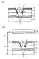
- Fig. 1 is a section view schematically showing an electron emitting device according to an embodiment.
- the barrier layer 3 is provided for preventing Al in the lower electrode 2 from diffusing into Si in the electron supply layer 4.
- the electron emitting device has a concave portion 7 formed by notching the upper electrode 6 and the insulating layer 5 to the electron supply layer 4 such that the electron supply layer 4 is exposed at the bottom surface (a portion 4a in Fig. 1 ) of the concave portion 7.
- a carbon layer 8 is formed to cover the upper electrode 6 and the concave portion 7 except for an inner portion 4b of the exposed surface 4a of the electron supply layer 4 and is in contact with an edge portion 4c of the exposed surface 4a.
- a crystal phase A is provided in the region of the electron supply layer 4 that is in contact with the carbon layer 8.
- a collector electrode 10 formed on a front substrate 9 is placed closer to the upper electrode 6 of the electron emitting device with a vacuum interposed between them.
- a voltage Vd is applied between the lower electrode 2 and the upper electrode 6 to cause electrons to be emitted from the upper electrode 6 and then to be collected by the collector electrode 10.
- a fluorescent layer 11 is formed as a light emitter on the collector electrode 10. The electrons are emitted from the electron emitting device toward the collector electrode 10 and are smashed against the fluorescent layer 11 to cause the fluorescent layer 11 to emit light.
- the concave portion 7 is formed by notching the upper electrode 6 and the insulating layer 5 to expose the electron supply layer 4 and has a conical shape with a gradually increasing diameter from the circular bottom surface to the top opening.
- the shape of the concave portion 7 is not limited thereto, and the bottom surface may be a circular shape, a square shape, or a linear shape, for example.
- the side of the concave portion 7 may be provided such that an angle ⁇ between the side wall of the insulating layer 5 and the surface of the electron supply layer 4 satisfies 0 ⁇ ⁇ ⁇ 135°.
- the concave portion 7 can be formed when ⁇ is larger than zero. If ⁇ is equal to or larger than 135°, however, the side wall of the concave portion 8 interferes with the formation of the carbon layer 8 on the concave portion 7 to prevent the carbon layer 8 from extending to the side wall and the outer edge portion of the bottom surface of the concave portion 7, which may preclude the formation of the continuous carbon layer 8. Since the device has a miniature structure, the continuous carbon layer 8 can be formed with sputtering or the like as long as ⁇ is equal to or smaller than 135°, and the resultant device can be driven properly.
- the concave portion 7 is used as an emission site, and electrons are emitted concentratedly in this portion during energization. This can maintain the amount of emitted electrons, while the insulating layer 5 can have a large thickness except the concave portion 7 to prevent a defect such as a pinhole in the insulating layer 5.
- the carbon layer 8 is formed on the upper electrode 6 and the concave portion 7 except for the inner portion 4b of the exposed surface 4a of the electron supply layer 4 such that the carbon layer 8 covers the upper electrode 6 and the inclined surface of the side wall of the concave portion 7 and is in contact with the edge portion 4c of the exposed surface 4a of the electron supply layer 4. In other words, the carbon layer 8 is in contact only with the edge portion 4c of the exposed surface 4a of the electron supply layer 4.
- the portion of the exposed surface 4a of the electron supply layer 4 where the electron supply layer 4 is in contact with the carbon layer 8 has a width which is less than 30% of the diameter of the exposed surface 4a from the outer edge, more preferably a width less than 25%. In such a range, an electric current during energization can be locally concentrated and the amount of emitted electrons can be maintained sufficiently.
- the carbon layer 8 Since the carbon layer 8 is in contact with the edge portion 4c of the exposed surface 4a of the electron supply layer 4 and is not in contact with the inner portion 4b, the electric current during energization is concentrated on the edge portion 4c of the exposed surface 4a and the current flow to the inner portion 4b is suppressed to increase the efficiency of electron emission. Heat production in the carbon layer 8 due to the energization is also limited to the edge portion 4c of the exposed surface 4a, so that the heat amount can be reduced. Since the heat production in the carbon layer 8 is concentrated on the edge portion 4c of the exposed surface 4a, the edge portion 4c of the exposed surface 4a of the electron supply layer 4 is crystallized and the inner portion 4b is prevented from crystallization. As a result, the crystal phase A can be provided in a confined region to reduce a volume change of the electron supply layer 4 to prevent damage or breakage of the device.
- Materials of the carbon layer 8 include carbon in the form of amorphous carbon, graphite, carbyne, fullerene (C 2n ), diamond-like carbon, carbon nanotube, carbon nanofiber, carbon nanohorn, carbon nanocoil, carbon nanoplate, and diamond, or a carbon compound such as ZrC, SiC, WC, MoC, and HfC.
- the carbon layer 8 preferably has a thickness of 0.1 to 100 nm, more preferably 0.1 to 60 nm.
- the carbon layer 8 having an extremely small thickness is difficult to provide uniformly, while the carbon layer having an extremely large thickness may increase a reactive current to reduce the efficiency of the device.
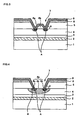
- Fig. 3 shows a modification of the carbon layer 8.
- a carbon layer 8 in Fig. 3 is in contact with an edge portion 4c of an exposed surface 4a of an electron supply layer 4 and is raised to have a domical shape 8a in an inner portion 4b.
- the carbon layer 8 having such a shape achieves similar effects to those in the device in Fig. 1 since the carbon layer 8 is not in contact with the inner portion 4b of the exposed surface 4a of the electron supply layer 4 and is in contact only with the edge portion 4c. Heat production in the carbon layer 8 during energization crystallizes only the edge portion 4c of the exposed surface 4a of the electron supply layer 4 and the inner portion 4b is prevented from crystallization.
- an interior 8b of the domical shape 8a of the carbon layer 8 is under vacuum.
- the vacuum insulation state in the interior 8b of the domical shape 8a favorably maintains insulation near the emission site to reduce a reactive current.
- the crystal phase A is formed at the edge portion 4c of the exposed surface 4a of the electron supply layer 4 in the region where the electron supply layer 4 is in contact with the carbon layer 8.
- the crystal phase A has a generally semicircular sectional shape in which the center of the semicircle corresponds to the point of the electron supply layer 4 in contact with the carbon layer 8, that is, the edge portion 4c of the electron supply layer 4, and the crystal phase A is formed in a ring shape along the circular edge portion 4c.
- the crystal phase A in the ring shape can be provided by specifying the point of contact of the electron supply layer 4 with the carbon layer 8 as the center of the semicircle and by setting a radius not exceeding the midpoint of the exposed surface 4a.
- the shape of the crystal phase A is not limited to the semicircular section, and the crystal phase A may be formed over the entire region near the surface closer to the insulating layer 5 except for the inner portion 4b of the exposed surface 4a of the electron supply layer 4.
- the particle diameter of the crystal phase A is not limited specifically but preferably ranges from 0.1 nm to the size corresponding to the region of the crystal phase A described above. A particle diameter smaller than 0.1 nm is beyond the resolution of a measurement apparatus, so that the adjustment of the particle diameter is difficult.
- the crystal phase A formed at the edge portion 4c of the exposed surface 4a of the electron supply layer 4 allows an electric current to be concentrated on the crystal phase A during energization, so that the amount of emitted electrons can be increased at a low voltage.
- the crystal phase A is formed locally in the region of the edge portion 4c of the exposed surface 4a of the electron supply layer 4 and is prevented from being formed in the inner portion 4b, which can reduce a volume change in the electron supply layer 4 to preclude breakage of the device.
- the generally semicircular sectional shape of the crystal phase A results from production of Joule heat by concentrating the electric current on the edge portion 4c of the exposed surface 4a of the electron supply layer 4 during energization. In other words, a reactive current is reduced during energization.
- the crystal phase A formed efficiently in this manner can reduce a volume change in the electrode supply layer 4 to prevent deformation or breakage of the device.
- a crystal phase B having a crystal particle diameter smaller than that of the crystal phase A and formed around the crystal phase A Since the crystal phase B is located away from the interface between the carbon layer 8 serving as a heat source and the electron supply layer 4, the crystal phase B is provided with a heat amount smaller than that in the crystal phase A and is formed to have the crystal particle diameter smaller than that of the crystal phase A. The amount of emitted electrons can be maintained when the crystal phase B is present around the crystal phase A in the electron supply layer 4 in this manner instead of the amorphous phase. In addition, since the crystal phase B has the small particle diameter, a volume change in the electron supply layer 4 can be reduced to prevent deformation or breakage of the device.
- the crystal phase B having the generally semicircular sectional shape with the center thereof corresponding to the central portion of the exposed surface 4a of the electron supply layer 4 results from the efficient formation of the crystal phase B by concentrating an electric current on the portion of contact of the carbon layer 8 with the electron supply layer 4 during energization to produce Joule heat therein.
- This structure can reduce a volume change in the electron supply layer 4 to prevent deformation and breakage of the device.
- Fig. 4 shows the horizontally semielliptical sectional shape since the crystal phase B is schematically shown, the crystal phase B may have a generally semicircular sectional shape having a circumference at a uniform distance from the center when the electron supply layer 4 is thickened in accordance with the size of the crystal phase B.
- the crystal phase B may have any crystal particle diameter as long as it is smaller than that of the crystal phase A, and preferably, the diameter is as small as approximately 0.1 nm.
- the crystal particle diameter of the crystal phase B may be increased to a level which is slightly smaller than that of the crystal phase A.
- the crystal phase B does not show significant volume expansion and is stabilized due to the small crystal particles.
- an electric current passes from the upper electrode 6 to the electron supply layer 4 to cause electrons to diffuse in the electron supply layer 4 and to flow to the upper electrode 6.
- the electric current is concentrated on the edge portion 4c of the exposed surface 4a of the electron supply layer 4, that is, the portion of contact of the carbon layer 8 with the electron supply layer 4 to increase the current density.
- the electrons are concentrated on this position to increase the amount of emitted electrons.
- the concentration of the electric current on the portion of contact of the carbon layer 8 with the electron supply layer 4 produces a large amount of Joule heat which produces the crystal phase A in the electron supply layer 4 along the edge portion 4c of the exposed surface 4a.
- the crystal phase A holds its form even when the temperature is reduced. Once the crystal phase A is formed, a current flow is promoted from the amorphous area to the crystal phase A when the current is concentrated on the portion of contact of the carbon layer 8 with the electron supply layer 4 during subsequent energization, so that the electric current can be more concentrated on that portion.
- the abovementioned steps result in the device in which part of an injected current tunnels through the insulating layer 5 to emit electrons from the concave portion 7. Traps are present at various levels in the insulating layer 5.
- the electrons injected from the electron supply layer 4 by thermal excitation flow through SiO x in the insulating layer 5 with hopping conduction, and some of the electrons are captured by the traps closer to the electron supply layer 4.
- the captured electrons serve as fixed charge to produce significant band bending in the insulating layer 5 closer to the vacuum to cause a high electric field.
- the high electric field changes the electrons into hot electrons having high energy which are emitted into the vacuum.
- the confined portion of contact of the carbon layer with the electron supply layer allows the electric current to be concentrated on that contact portion to improve the efficiency of electron emission.
- the Joule heat in the carbon layer during energization is concentrated on the contact portion, so that the crystal phase in the electron supply layer is locally formed at the edge portion of the exposed surface to reduce a volume change due to crystallization to prevent damage to the device while the efficiency of electron emission is maintained.
- the method of manufacturing the electron emitting device includes forming the lower electrode, the barrier layer, the electron supply layer, the insulating layer, and the upper electrode in order over the substrate, forming the concave portion by notching the insulating layer and the upper electrode, forming the carbon layer thereon, and stripping part of the carbon layer from the inner portion at the bottom surface of the concave portion.
- part of the carbon layer on the inner portion at the bottom surface of the concave portion is raised away from the electron supply layer into the domical shape.
- the carbon layer may be formed on the upper electrode and on the edge portion at the bottom surface of the concave portion with masking using a mask conforming to the inner portion at the bottom surface of the concave portion.
- the insulating layer and the upper electrode may be formed with masking to provide the concave portion.
- the layer deposition may be performed by using a physical deposition method or a chemical deposition method.
- the physical deposition method is known as PVD (Physical Vapor Deposition) which includes vacuum deposition, molecular beam epitaxy, sputtering, ionization vapor deposition, and laser ablation.
- the chemical deposition method is known as CVD (Chemical Vapor Deposition) which includes thermal CVD, plasma CVD, and OMCVD (Organic-Metal Chemical Vapor Deposition). Among them, the sputtering of the physical deposition method is particularly preferable.
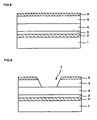
- Fig. 5 to Fig. 12 show an example of the method of manufacturing the electron emitting device.
- the lower electrode 2 made of Al and the barrier layer 3 made of TiN are deposited with sputtering over the substrate 1 made of Si and having a thermal oxidation film formed thereon.
- the amorphous electron supply layer 4 including Si doped with B at a concentration of 1.1% is deposited on the barrier layer 3 with sputtering.
- the insulating layer 5 made of SiO x is deposited on the electron supply layer 4 with plasma CVD using TEOS (Tetra ethoxysilane) as a material gas.
- the insulating layer 5 may be formed with sputtering instead.
- the upper electrode 6 made of W is deposited on the insulating layer 5 with sputtering.
- the concave portion 7 is patterned by partially removing the upper electrode 6 and the insulating layer 5 to the electrode supply layer 4 through a photoetching process. After the concave portion 7 is formed, the carbon layer 8 is deposited with sputtering on the upper electrode 6 and the concave portion 7 as shown in Fig. 10 .
- a voltage is applied between the upper electrode 6 and the lower electrode 2 and the energization produces Joule heat in the portion of the carbon layer 8 in contact with the electron supply layer 4.
- the Joule heat burns and strips the portion of the carbon layer 8 in the inner portion 4b of the exposed surface 4a of the electron supply layer 4. It is contemplated that the electric current passes while the carbon layer 8 is in contact with the exposed surface 4a and that the Joule heat is produced in the entire carbon layer 8 in contact with the exposed surface 4a, thereby burning and stripping the portion of the carbon layer 8 placed in the inner portion 4b of the exposed surface 4a.
- the portion of the carbon layer 8 in the inner portion 4b of the exposed surface 4a of the electron supply layer 4 is raised due to thermal expansion to have the domical shape 8a.
- the domical shape 8a shown in Fig. 12 can be provided, for example by forming a recess in the edge portion 4c of the exposed surface 4a such that the electric current tends to be concentrated in that recess.
- the stripped state as shown in Fig. 11 can be provided.
- the stripped state or the domical shape of the carbon layer 8 can also be controlled by locally changing the degree of doping in the electron supply layer.
- the portion of the carbon layer 8 separated from the inner portion 4b of the exposed surface 4a of the electron supply layer 4 serves as the domical shape 8a and is fixed on the device to eliminate the need to remove the separated carbon layer 8 with cleaning or the like.
- pretreatment can be performed with plasma processing such as RF plasma etching, cleaning, or heat treatment such as baking. Then, the carbon layer 8 is formed, and when the portion of the carbon layer 8 is stripped from the inner portion 4b of the exposed surface 4a of the electron supply layer 4, the stripping of the carbon layer 8 can be promoted by the pretreatment.
- the cleaning include heating H 2 SO 4 cleaning, dilute HF solution cleaning, pure water cleaning, acetone cleaning, and alcohol cleaning.
- the pretreatment may damage the previously deposited layers, especially the outermost layer, but the pretreatment can be performed under controlled conditions in view of the possible damage.
- the Joule heat in the carbon layer 8 produced during the energization is transferred to the edge portion 4c of the exposed surface 4a of the electron supply layer 4 to heat and crystallize the region of the electron supply layer 4 that includes the edge portion 4c at the center, thereby forming the crystal phase A.
- the voltage in this case is applied with sweep to be gradually increased from low to high levels until the diode current is reduced or an inflection point is found in the diode current and an emission current flows.
- the Joule heat is concentrated on the portion of contact of the electron supply layer 4 with the carbon layer 8, that is, the edge portion 4c of the exposed surface 4a of the electron supply layer 4, and the heat is transferred radially from the edge portion 4c.
- the size of the crystal phase A can be adjusted by controlling the amount of heat produced at the edge portion 4c of the exposed surface 4 of the electron supply layer 4.
- the heat amount can be controlled by the applied voltage and the sweep rate of voltage.
- a plurality of concave portions 7 are typically provided over the substrate 1 to constitute the device, and the heat amount can be controlled by the number (density) of the concave portions 7 and the arrangement thereof.
- the size of the crystal phase A can also be adjusted by controlling the sweep rate of voltage during energization. As the sweep rate is lower, the heat is transferred to a region outside the concave portion 7 to increase easily the temperature of the concave portion 7 to allow crystallization of the electron supply layer 4 at a lower voltage. As the sweep rate is too high, a large electric current may break the device. For those reasons, the sweep rate can be set in a range from 0.001 to 5 V/sec to prevent extreme Joule heat production to adjust the size of the crystal phase A. A higher sweep rate than those in the range may be used, and in such a case, the applied voltage preferably has a pulse shape with a specific width.
- the region of the crystal phase A in the electron supply layer 4 can be controlled to prevent breakage of the device by controlling the current amount passing through the device during energization, that is, by imposing a limit on the electric current. This can also control the deformation amount of the carbon layer 8 in the stripping or raising thereof.
- a driving circuit such as a transistor can be used to set the current limit.
- the shape and size of the crystal phase A can also be controlled by adjusting the angle ( ⁇ ) of the concave portion 7 and the thickness of the insulating layer 5.
- the amount of heat at the edge portion 4c of the exposed surface 4a of the electron supply layer 4 may be adjusted similarly to the formation of the crystal phase A.
- adjustment is performed similarly to the formation of the crystal phase A.
- the steps from the stripping of the carbon layer 8 to the formation of the crystal phase A are described on the basis of a mechanism generally called self-control.
- the Joule heat produced by the energization spontaneously raises the carbon layer 8 to reduce the area of contact of the carbon layer 8 with the electron supply layer 4 to avoid extreme part of the Joule heat.
- the stripping of the carbon layer 8 shown in Fig. 11 occurs when the extreme Joule heat production cannot be avoided by the self-control, and the Joule heat burns the portion of the carbon layer 8 inside the concave portion 7.
- the raising of the carbon layer 8 shown in Fig. 12 occurs when the extreme heat is avoided by the self-control.
- the portion of the carbon layer 8 inside the concave portion 7 is formed into the domical shape 8a to produce the hollow region 8b.
- the electric current is concentrated on the portion of contact of the carbon layer 8 with the electron supply layer 4 to crystallize the electron supply layer 4 immediately below to form the crystal phase A.
- the self-control can significantly reduce breakage of the device to manufacture the electron emitting device more stably.
- the control of the adhesion strength of the carbon layer 8 and the inner portion 4b is important.
- the pretreatment such as etching, cleaning, or heat treatment can be performed on the surface of the layers before the formation of the carbon layer 8 as described above to control the adhesion strength of the carbon layer 8.
- the adhesion strength of the carbon layer 8 and the electron supply layer 4 can also be adjusted by controlling the deposition conditions of the carbon layer 8 or by changing the material of the carbon layer 8.
- the adhesion strength of the carbon layer 8 can be controlled from the structural aspects by changing the area of contact or the shapes of the carbon layer 8 and the upper electrode 6 or the electron supply layer 4.
- the bottom surface of the concave portion 7 can be formed in a multistage structure or a dimple structure to control the adhesion strength.
- the concave portion 7 can be formed in a circular shape, an elliptical shape, an oval shape, a polygonal shape, or a closed curve shape to control the adhesion strength.
- the control of the adhesion strength of the carbon layer 8 can prevent stripping or raising of the portion of the carbon layer 8 other than the portion thereof located in the concave portion 7 and can realize the stripping or raising of the portion of the carbon layer 8 only in the inner portion at the bottom surface of the concave portion 7.
- the crystal phase A in the electron supply layer 4 preferably has a small area in order to prevent breakage of the electron emitting device.
- the area of contact of the carbon layer 8 with the electron supply layer 4 can be limited to confine the region where the crystal phase A is formed to near the contact portion.
- the current is concentrated on the contact portion due to the small contact area to provide a large amount of Joule heat.
- the structure in which the small area of the carbon layer 8 is in contact with the electron supply layer 4 enables prevention of crystallization of the whole electron supply layer 4 with the use of the reduced injected current and allows concentration of the current on the contact area to provide a large amount of Joule heat to form the crystal phase A locally.
- the structure is advantageous in providing miniature electron emitting devices.
- the confined region of crystallization leads to manufacture of an device which operates at a low current. In other words, the power consumption can be reduced.
- the electron emitting device typically emits electrons into vacuum-sealed space, the prevention of the breakage of the device reduces gas emission to increase the life of the apparatus as a whole.
- a particularly effective material of the electron supply layer is amorphous silicone (a-Si) doped with a group IIIb or Vb element and deposited with the abovementioned sputtering or CVD. It is also possible to use hydrogenated amorphous silicone in which a-Si dangling bond is terminated by hydrogen, hydrogenated amorphous silicon carbide in which carbon substitutes for part of Si, hydrogenated amorphous silicon nitride in which nitrogen substitutes for part of Si, an elemental semiconductor and a compound semiconductor of a IV, a III-V, or a II-VI group such as germanium, Ge-Si, silicon carbide, gallium arsenide, indium phosphide, cadmium selenide, and CuInTe2 instead of Si, or silicon doped with boron, gallium, phosphorous, indium, arsenic, or antimony.
- metal such as Al, Au, Ag, and Cu
- metal such as Al, Au, Ag, and Cu
- Sc Ti, Cr, Mn, Fe, Co, Ni, Zn, Ga, Y, Zr, Nb, Mo, Tc, Ru, Rh, Pd, Cd, Ln, Sn, Ta, W, Re, Os, Ir, Pt, Tl, Pb, La, Ce, Pr, Nd, Pm, Sm, Eu, Gd, Tb, Dy, Ho, Er, Tm, Yb, and Lu.
- the electron supply layer preferably has a thickness of 0.1 nm to 10 ⁇ m.
- a thickness less than 0.1 nm may result in difficulty in forming a uniform layer to prevent proper formation of the crystal phase A, while a thickness larger than 10 ⁇ m is disadvantageous in that a long deposition time is required.
- the doping concentration of B preferably ranges from 0.1 to 20.0%. Although a lower doping concentration of B can reduce a defective hollow to prevent the breakage of the device, an extremely low doping concentration of B leads to a high resistance value to need application of a high voltage.
- SiO x (x represents an atomic ratio) described above is particularly effective, and it is also possible to use a metal oxide or a metal nitride including LiO x , LiN x , NaO x , KO x , RbO x , CsO x , BeO x , MgO x , MgN x , CaO x , CaN x , SrO x , BaO x , ScO x , YO x , YN x , LaO x , LaN x , CeO x , PrO x , NdO x , SmO x , EuO x , GdO x , TbO x , DyO x , HoO x , ErO x , TmO x , YbO x , LuO x , TiO x ,
- a metal composite oxide such as LiAlO 2 , Li 2 SiO 3 , Li 2 TiO 3 , Na 2 Al 22 O 34 , NaFeO 2 , Na 4 SiO 4 , K 2 SiO 3 , K 2 TiO 3 , K 2 WO 4 , Rb 2 CrO 4 , CS 2 CrO 4 , MgAl 2 O 4 , MgFe 2 O 4 , MgTiO 3 , CaTiO 3 , CaWO 4 , CaZrO 3 , SrFe 12 O 19 , SrTiO 3 , SrZrO 3 , BaAl 2 O 4 , BaFe 12 O 19 , BaTiO 3 , Y 3 Al 5 O 12 , Y 3 Fe 5 O 12 , LaFeO 3 , La 3 Fe 5 O 12 , La 2 Ti 2 O 7 , CeSnO 4 , CeTiO 4 , Sm 3 Fe 5 O 12 , EuFeO 3
- insulating layer examples include a sulfide such as FeS, Al 2 S 3 , MgS, and ZnS, a fluoride such as LiF, MgF 2 , and SmF 3 , a chloride such as HgCl, FeCl 2 , and CrCl 3 , a bromide such as AgBr, CuBr, and MnBr 2 , an iodide such as PbI 2 , CuI, and FeI 2 , a lanthanoid boride compound such as LaB 6 and CeB 6 , a metal boride such as TiB 2 , ZrB 2 , and HfB 2 , or a metallic oxynitride such as SiAlON.
- a sulfide such as FeS, Al 2 S 3 , MgS, and ZnS
- a fluoride such as LiF, MgF 2 , and SmF 3
- a chloride such as HgCl
- insulating layer Other effective materials for the insulating layer include carbon such as diamond and fullerene (C 2n ) or a metal carbide such as Al 4 C 3 , B 4 C, CaC 2 , Cr 3 C 2 , Mo 2 C, MoC, NbC, SiC, TaC, TiC, VC, W 2 C, WC, and ZrC.
- Fullerene (C 2n ) is a spherical mesh molecule made only of carbon atoms and typified by C 60 , and includes C 32 to C 960 . In the above chemical formulas, x in O x or N x represents an atomic ratio.
- the insulating layer has a thickness of 50 nm or larger, more preferably approximately 100 nm to 1 ⁇ m, except the concave portion.
- the concave portion serves as the emission site, the amount of emitted electrons can be increased even when the insulating layer has a large thickness except the concave portion. Since the large thickness of the insulating layer reduces a leak current, the current is not wasted and can be used for producing the required Joule heat accordingly. If the insulating layer has an extremely large thickness, step coverage is poor in the subsequent layers and the amount of emitted electrons may be reduced.
- the plasma CVD using TEOS can reduce defects which may cause a leak current and can form the insulating layer having a thickness of 50 nm.
- the sputtering can form the insulating layer having a thickness of 100 nm to 1 ⁇ m to prevent defects favorably.
- the material of the lower electrode 2 it is possible to use a material generally used for IC wiring such as Au, Pt, and W, a three-layer structure including chromium, nickel, and chromium, an alloy of Al an Nd, an alloy of Al and Mo, and an alloy of Ti and N, in addition to Al described above.
- a material generally used for IC wiring such as Au, Pt, and W
- a three-layer structure including chromium, nickel, and chromium, an alloy of Al an Nd, an alloy of Al and Mo, and an alloy of Ti and N, in addition to Al described above.
- the material of the upper electrode 6 it is possible to use effectively metal such as Pt, Au, Ru, and Ir in addition to W described above. It is also possible to use Be, C, Al, Si, Sc, Ti, V, Br, Mn, Fe, Co, Ni, Cu, Zn, Ga, Y, Zr, Nb, Mo, Tc, Rh, Pd, Ag, Cd, In, Sn, Ta, Re, So, Tl, Pb, La, Ce, Pr, Nd, Pm, Sm, Eu, Gd, Tb, Dy, Ho, Er, Tm, Yb, and Lu.
- effectively metal such as Pt, Au, Ru, and Ir in addition to W described above. It is also possible to use Be, C, Al, Si, Sc, Ti, V, Br, Mn, Fe, Co, Ni, Cu, Zn, Ga, Y, Zr, Nb, Mo, Tc, Rh, Pd, Ag, Cd, In, Sn, Ta, Re, So, Tl, Pb, La
- Example 2 a lower electrode 2 made of Al and a barrier layer 3 made of TiN were deposited with sputtering to have thicknesses of 600 nm and 150 nm, respectively, over a substrate 1 made of Si and having a thermal oxidation film formed thereon.
- An electron supply layer 4 made of amorphous Si doped with B at a concentration of 1.1% was deposited thereon with sputtering to have a thickness of 8.4 ⁇ m.
- An insulating layer 5 made of SiO x was deposited thereon with plasma CVD using TEOS to have a thickness of 300 nm.
- An upper electrode 6 made of W was deposited thereon with sputtering to have a thickness of 60 nm.
- the upper electrode 6 and the insulating layer 5 were partially removed to the electron supply layer 4 through a photoetching process to form a concave portion 7 having a depth of 360 nm.
- the concave portion 7 was formed such that an angle ⁇ between the side of the insulating layer 5 and the electron supply layer 4 ranged from 70 to 100°.
- Sixteen concave portions 7 were formed in a 4-by-4 matrix with a 10- ⁇ m pitch over the substrate 1.
- baking was performed at 350°C for two hours in a vacuum as pretreatment before the formation of a carbon layer 8.
- the carbon layer 8 was deposited with sputtering to have a thickness of 60 nm on the upper electrode 6 and the concave portion 7.
- Comparative Example an device was formed through the same steps as those in Example described above except that baking was not performed as pretreatment before formation of carbon.
- a collector electrode 10 was placed above the upper electrode 6.
- the upper electrode 6 was located 2mm from the collector electrode 10. While a voltage of 1 kV was applied between the upper electrode 6 and the collector electrode 10, a voltage up to 20 v was applied between the lower electrode 2 and the upper electrode 6 at a sweep rate of 0.33 V/s.
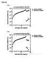
- the sectional shape after the energization was observed with a TEM, while the surface shape was observed with an SEM. I-V characteristics per site were measured and the results thereof are shown in Figs. 13(a) and 13(b).
- Fig. 13(a) shows the device in Example
- Fig. 13 (b) shows the device in Comparative Example.
- the conditions in the voltage application including the sweep rate in the above energization provide illustrative ones and the present invention is not limited thereto.
- the carbon layer in Comparative Example was in contact with the entirety of the exposed surface of the electron supply layer.
- a crystal phase in the electron supply layer extended as deep as 5.0 ⁇ m from the upper surface of the electron supply layer to show the crystallization in a wider region than in Example. It is thought that this is because pretreatment was not performed before the carbon layer was formed, so that the self-control did not function and the area of the electron supply layer in contact with the carbon layer was increased, thereby subjecting the electron supply layer to extreme Joule heat from the carbon layer during energization to widen the crystal phase in the electron supply layer.
- Example it is thought that the self-control functioned as seen from the abovementioned TEM observation and SEM observation, so that the carbon layer 8 was raised from the inner portion 4b of the exposed surface 4a of the electron supply layer 4 to concentrate the electric current on the edge portion 4c of the exposed surface 4a during the energization to achieve the electron emission efficiently.
- the electron emitting device includes an amorphous electron supply layer, an insulating layer formed on the electron supply layer, and an electrode formed on the insulating layer, the electron emitting device emitting electrons when an electric field is applied between the electron supply layer and the electrode, wherein the electron emitting device includes a concave portion provided by notching the electrode and the insulating layer to expose the electron supply layer, and a carbon layer covering the electrode and the concave portion except for an inner portion of an exposed surface of the electron supply layer and being in contact with an edge portion of the exposed surface of the electron supply layer, thereby improving the efficiency of electron emission and preventing damage to the device.
- a display apparatus using the electron emitting device according to the present invention includes an electron emitting device and a light emitter which emits light when electrons emitted from the electron emitting device are smashed against the light emitter, wherein the electron emitting device is the abovementioned electron emitting device, thereby improving the efficiency of electron emission and preventing damage to the device. It is thus possible to provide a display apparatus which achieves energy savings and long life.
- the method of manufacturing the electron emitting device includes an amorphous electron supply layer, an insulating layer formed on the electron supply layer, and an electrode formed on the insulating layer, the electron emitting device emitting electrons when an electric field is applied between the electron supply layer and the electrode, the method including a step of forming a concave portion by notching the electrode and the insulating layer to expose the electron supply layer, and a step of forming a carbon layer covering the electrode and the concave portion except for an inner portion of an exposed surface of the electron supply layer and being in contact with an edge portion of the exposed surface of the electron supply layer, thereby improving the efficiency of electron emission and preventing damage to the device.
Landscapes
- Engineering & Computer Science (AREA)
- Chemical & Material Sciences (AREA)
- Nanotechnology (AREA)
- Manufacturing & Machinery (AREA)
- Physics & Mathematics (AREA)
- Mathematical Physics (AREA)
- Theoretical Computer Science (AREA)
- Crystallography & Structural Chemistry (AREA)
- Cold Cathode And The Manufacture (AREA)
- Cathode-Ray Tubes And Fluorescent Screens For Display (AREA)
- Electrodes For Cathode-Ray Tubes (AREA)
Claims (13)
- Elektronenemissionsvorrichtung mit einer amorphen Elektronenzufuhrschicht (4), einer Isolationsschicht (5), die auf der Elektronenzufuhrschicht (4) ausgebildet ist, und einer Elektrode (6), die auf der Isolationsschicht (5) ausgebildet ist, wobei die Elektronenemissionsvorrichtung Elektronen emittiert, wenn ein elektrisches Feld zwischen der Elektronenzufuhrschicht (4) und der Elektrode (6) angelegt wird,
wobei die Elektronenemissionsvorrichtung einen konkaven Abschnitt (7), der durch Kerben der Elektrode (6) und der Isolationsschicht (5) bereitgestellt wird, um die Elektronenzufuhrschicht (4) freizulegen, und eine Kohlenstoffschicht (8) aufweist, die die Elektrode (6) bedeckt, dadurch gekennzeichnet, dass die Kohlenstoffschicht auch den konkaven Abschnitt (7) mit der Ausnahme eines inneren Abschnitts (4b) einer freiliegenden Oberfläche (4a) der Elektronenzufuhrschicht (4) bedeckt und mit einem Kantenabschnitt (4c) der freiliegenden Oberfläche (4a) der Elektronenzufuhrschicht (4) in Kontakt steht. - Elektronenemissionsvorrichtung nach Anspruch 1, wobei die Kohlenstoffschicht (8) am inneren Abschnitt (4b) der freiliegenden Oberfläche (4a) der Elektronenzufuhrschicht (4) eine Kuppelform (8a) aufweist.
- Elektronenemissionsvorrichtung nach Anspruch 2, wobei die Kuppelform (8a) einen Vakuuminnenraum (8b) aufweist.
- Elektronenemissionsvorrichtung nach einem der Ansprüche 1 bis 3, wobei die Elektronenzufuhrschicht (4) eine Kristallphase (A) aufweist, die mit der Kohlenstoffschicht (8) in Kontakt steht.
- Elektronenemissionsvorrichtung nach Anspruch 4, wobei die Kristallphase (A) eine im Wesentlichen halbkreisförmige Querschnittsform aufweist.
- Elektronenemissionsvorrichtung nach Anspruch 4 oder 5, wobei die Elektronenzufuhrschicht (4) eine Kristallphase (B) um die Kristallphase (A) aufweist, wobei die erstgenannte Kristallphase (B) Kristallteilchen mit einem kleineren Durchmesser als dem der letztgenannten Kristallphase (A) aufweist.
- Elektronenemissionsvorrichtung nach Anspruch 6, wobei die Kristallphase (B) mit dem kleineren Durchmesser eine im Wesentlichen halbkreisförmige Querschnittsform aufweist.
- Anzeigevorrichtung, die eine Elektronenemissionsvorrichtung und einen Lichtemitter (11) aufweist, der Licht emittiert, wenn aus der Elektronenemissionsvorrichtung emittierte Elektronen gegen den Lichtemitter (11) geworfen werden, wobei die Elektronenemissionsvorrichtung die Elektronenemissionsvorrichtung nach einem der Ansprüche 1 bis 7 ist.
- Verfahren zum Herstellen einer Elektronenemissionsvorrichtung mit einer amorphen Elektronenzufuhrschicht (4), einer Isolationsschicht, die auf der Elektronenzufuhrschicht (4) ausgebildet ist, und einer Elektrode (6), die auf der Isolationsschicht (5) ausgebildet ist, wobei die Elektronenemissionsvorrichtung Elektronen emittiert, wenn ein elektrisches Feld zwischen der Elektronenzufuhrschicht (4) und der Elektrode (6) angelegt wird, wobei das Verfahren aufweist:einen Schritt des Bildens eines konkaven Abschnitts (7) durch Kerben der Elektrode (6) und der Isolationsschicht (5), um die Elektronenzufuhrschicht (4) freizulegen, und einen Schritt des Bildens einer Kohlenstoffschicht (8), die die Elektrode (6) und den konkaven Abschnitt (7) mit der Ausnahme eines inneren Abschnitts (4b) einer freiliegenden Oberfläche (4a) der Elektronenzufuhrschicht (4) bedeckt und mit einem Kantenabschnitt (4c) der freiliegenden Oberfläche (4a) der Elektronenzufuhrschicht (4) in Kontakt steht.
- Verfahren zum Herstellen einer Elektronenemissionsvorrichtung nach Anspruch 9, wobei der Schritt des Bildens einer Kohlenstoffschicht (8) das Bilden der Kohlenstoffschicht (8) auf der Elektrode (6) und dem konkaven Abschnitt (7), das Leiten eines elektrischen Stroms zwischen der Elektronenzufuhrschicht (4) und der Elektrode (6) und das Abstreifen der Kohlenstoffschicht vom inneren Abschnitt (4b) der freiliegenden Oberfläche (4a) der Elektronenzufuhrschicht (4) durch Joule-Wärme aufweist, die von der Kohlenstoffschicht (8) erzeugt wird.
- Verfahren zum Herstellen einer Elektronenemissionsvorrichtung nach Anspruch 9, wobei der Schritt des Bildens einer Kohlenstoffschicht (8) das Bilden der Kohlenstoffschicht (8) auf der Elektrode (6) und dem konkaven Abschnitt (7), das Leiten eines elektrischen Stroms zwischen der Elektronenzufuhrschicht (4) und der Elektrode (6), und das Anheben der Kohlenstoffschicht (8) auf dem inneren Abschnitt (4b) der freiliegenden Oberfläche (4a) der Elektronenzufuhrschicht (4) zu einer Kuppelform (8a) durch Joule-Wärme aufweist, die von der Kohlenstoffschicht (8) erzeugt wird.
- Verfahren zum Herstellen einer Elektronenemissionsvorrichtung nach einem der Ansprüche 9 bis 11, wobei eine Ätzbehandlung, eine Reinigungsbehandlung oder eine Wärmebehandlung an der freiliegenden Oberfläche (4a) der Elektronenzufuhrschicht (4) durchgeführt wird, bevor die Kohlenstoffschicht (8) gebildet wird.
- Verfahren zum Herstellen einer Elektronenemissionsvorrichtung nach einem der Ansprüche 9 bis 12, das ferner einen Schritt des Leitens eines elektrischen Stroms zwischen der Elektronenzufuhrschicht (4) und der Elektrode (6) und das Kristallisieren eines Bereichs der Elektronenzufuhrschicht (4), der mit der Kohlenstoffschicht in Kontakt steht, durch Joule-Wärme aufweist, die von der Kohlenstoffschicht (8) erzeugt wird.
Applications Claiming Priority (2)
| Application Number | Priority Date | Filing Date | Title |
|---|---|---|---|
| JP2006096990 | 2006-03-31 | ||
| PCT/JP2007/056214 WO2007114103A1 (ja) | 2006-03-31 | 2007-03-26 | 電子放出素子、電子放出素子を用いた表示装置及び電子放出素子の製造方法 |
Publications (4)
| Publication Number | Publication Date |
|---|---|
| EP2006875A2 EP2006875A2 (de) | 2008-12-24 |
| EP2006875A9 EP2006875A9 (de) | 2009-07-22 |
| EP2006875A4 EP2006875A4 (de) | 2010-06-09 |
| EP2006875B1 true EP2006875B1 (de) | 2011-09-28 |
Family
ID=38563372
Family Applications (1)
| Application Number | Title | Priority Date | Filing Date |
|---|---|---|---|
| EP07739652A Ceased EP2006875B1 (de) | 2006-03-31 | 2007-03-26 | Elektronenemissionselement, anzeige mit dem elektronenemissionselement und verfahren zur herstellung des elektronenemissionselements |
Country Status (4)
| Country | Link |
|---|---|
| US (1) | US7994698B2 (de) |
| EP (1) | EP2006875B1 (de) |
| JP (2) | JP4959680B2 (de) |
| WO (1) | WO2007114103A1 (de) |
Families Citing this family (6)
| Publication number | Priority date | Publication date | Assignee | Title |
|---|---|---|---|---|
| JP2010245113A (ja) * | 2009-04-01 | 2010-10-28 | Sanyo Electric Co Ltd | 固体電解コンデンサ |
| WO2011074038A1 (ja) * | 2009-12-17 | 2011-06-23 | パイオニア株式会社 | 電子放出素子およびこれを備えた撮像装置 |
| JP5328939B2 (ja) * | 2010-01-07 | 2013-10-30 | パイオニア株式会社 | 電子放出素子およびこれを備えた撮像装置 |
| JP5994271B2 (ja) * | 2012-02-10 | 2016-09-21 | 国立大学法人東北大学 | 電子ビーム発生装置、電子ビーム照射装置、電子ビーム露光装置、および製造方法 |
| US11355301B2 (en) * | 2018-11-12 | 2022-06-07 | Peking University | On-chip micro electron source and manufacturing method thereof |
| CN109285740B (zh) * | 2018-11-12 | 2024-02-09 | 北京大学 | 一种片上微型电子源及其制造方法 |
Family Cites Families (3)
| Publication number | Priority date | Publication date | Assignee | Title |
|---|---|---|---|---|
| JP3765671B2 (ja) * | 1998-08-10 | 2006-04-12 | パイオニア株式会社 | 電子放出素子及びこれを用いた電子放出表示装置 |
| JP3874396B2 (ja) * | 2000-01-13 | 2007-01-31 | パイオニア株式会社 | 電子放出素子及びその製造方法並びに電子放出素子を用いた表示装置 |
| WO2003049132A1 (en) | 2001-12-06 | 2003-06-12 | Pioneer Corporation | Electron emitting device and method of manufacturing the same and display apparatus using the same |
-
2007
- 2007-03-26 JP JP2008508533A patent/JP4959680B2/ja active Active
- 2007-03-26 WO PCT/JP2007/056214 patent/WO2007114103A1/ja not_active Ceased
- 2007-03-26 US US12/225,798 patent/US7994698B2/en not_active Expired - Fee Related
- 2007-03-26 EP EP07739652A patent/EP2006875B1/de not_active Ceased
-
2011
- 2011-05-11 JP JP2011106086A patent/JP5171988B2/ja not_active Expired - Fee Related
Also Published As
| Publication number | Publication date |
|---|---|
| JP5171988B2 (ja) | 2013-03-27 |
| EP2006875A2 (de) | 2008-12-24 |
| WO2007114103A1 (ja) | 2007-10-11 |
| JPWO2007114103A1 (ja) | 2009-08-13 |
| JP2011151044A (ja) | 2011-08-04 |
| JP4959680B2 (ja) | 2012-06-27 |
| EP2006875A9 (de) | 2009-07-22 |
| US20090284129A1 (en) | 2009-11-19 |
| EP2006875A4 (de) | 2010-06-09 |
| US7994698B2 (en) | 2011-08-09 |
Similar Documents
| Publication | Publication Date | Title |
|---|---|---|
| EP0911854B1 (de) | Elektronenemissionsvorrichtung und Anzeigevorrichtung unter Verwendung derselben | |
| US5962959A (en) | Electron emission device and display device for emitting electrons in response to an applied electric field using the electron emission device | |
| US6023124A (en) | Electron emission device and display device using the same | |
| US6166487A (en) | Electron emission device and display device using the same | |
| US5990605A (en) | Electron emission device and display device using the same | |
| US6066922A (en) | Electron emission device and display device using the same | |
| JP4068564B2 (ja) | 電子放出素子及び表示装置 | |
| US6400070B1 (en) | Electron emission device and display device using the same | |
| EP0896355B1 (de) | Elektronenemissionsvorrichtung und Anzeigevorrichtung unter Verwendung derselben | |
| EP0865062B1 (de) | Herstellungsverfahren einer Elektronenemissionsvorrichtung und Anzeigevorrichtung | |
| JP3765671B2 (ja) | 電子放出素子及びこれを用いた電子放出表示装置 | |
| EP2006875B1 (de) | Elektronenemissionselement, anzeige mit dem elektronenemissionselement und verfahren zur herstellung des elektronenemissionselements | |
| US6144155A (en) | Electron emission device and display device using the same | |
| US20080211401A1 (en) | Electron Emission Device And Manufacturing Method Of The Same | |
| US6278230B1 (en) | Electron emission device and display device using the same | |
| US6147443A (en) | Electron emission device and display device using the same | |
| JP3698382B2 (ja) | 電子放出素子及びこれを用いた表示装置 | |
| JP2004288651A (ja) | 電子放出素子及びこれを用いた表示装置 |
Legal Events
| Date | Code | Title | Description |
|---|---|---|---|
| PUAI | Public reference made under article 153(3) epc to a published international application that has entered the european phase |
Free format text: ORIGINAL CODE: 0009012 |
|
| PUAB | Information related to the publication of an a document modified or deleted |
Free format text: ORIGINAL CODE: 0009199EPPU |
|
| 17P | Request for examination filed |
Effective date: 20081029 |
|
| AK | Designated contracting states |
Kind code of ref document: A2 Designated state(s): DE FR GB |
|
| DAX | Request for extension of the european patent (deleted) | ||
| RBV | Designated contracting states (corrected) |
Designated state(s): DE FR GB |
|
| A4 | Supplementary search report drawn up and despatched |
Effective date: 20100507 |
|
| RAP1 | Party data changed (applicant data changed or rights of an application transferred) |
Owner name: PIONEER CORPORATION |
|
| RIC1 | Information provided on ipc code assigned before grant |
Ipc: H01J 31/12 20060101ALI20110104BHEP Ipc: H01J 29/04 20060101ALI20110104BHEP Ipc: H01J 9/02 20060101ALI20110104BHEP Ipc: H01J 1/312 20060101AFI20110104BHEP |
|
| RTI1 | Title (correction) |
Free format text: ELECTRON EMISSION ELEMENT, DISPLAY COMPRISING THE ELECTRON EMISSION ELEMENT, AND METHOD OF FABRICATING THE ELECTRON EMISSION ELEMENT |
|
| GRAP | Despatch of communication of intention to grant a patent |
Free format text: ORIGINAL CODE: EPIDOSNIGR1 |
|
| GRAS | Grant fee paid |
Free format text: ORIGINAL CODE: EPIDOSNIGR3 |
|
| GRAA | (expected) grant |
Free format text: ORIGINAL CODE: 0009210 |
|
| AK | Designated contracting states |
Kind code of ref document: B1 Designated state(s): DE FR GB |
|
| REG | Reference to a national code |
Ref country code: GB Ref legal event code: FG4D |
|
| REG | Reference to a national code |
Ref country code: DE Ref legal event code: R096 Ref document number: 602007017523 Country of ref document: DE Effective date: 20111201 |
|
| REG | Reference to a national code |
Ref country code: GB Ref legal event code: 746 Effective date: 20120125 |
|
| PLBE | No opposition filed within time limit |
Free format text: ORIGINAL CODE: 0009261 |
|
| STAA | Information on the status of an ep patent application or granted ep patent |
Free format text: STATUS: NO OPPOSITION FILED WITHIN TIME LIMIT |
|
| 26N | No opposition filed |
Effective date: 20120629 |
|
| REG | Reference to a national code |
Ref country code: DE Ref legal event code: R097 Ref document number: 602007017523 Country of ref document: DE Effective date: 20120629 |
|
| REG | Reference to a national code |
Ref country code: DE Ref legal event code: R084 Ref document number: 602007017523 Country of ref document: DE |
|
| REG | Reference to a national code |
Ref country code: DE Ref legal event code: R119 Ref document number: 602007017523 Country of ref document: DE Ref country code: DE Ref legal event code: R409 Ref document number: 602007017523 Country of ref document: DE |
|
| REG | Reference to a national code |
Ref country code: DE Ref legal event code: R409 Ref document number: 602007017523 Country of ref document: DE |
|
| REG | Reference to a national code |
Ref country code: DE Ref legal event code: R084 Ref document number: 602007017523 Country of ref document: DE Effective date: 20140923 Ref country code: DE Ref legal event code: R119 Ref document number: 602007017523 Country of ref document: DE Effective date: 20141003 Ref country code: DE Ref legal event code: R084 Ref document number: 602007017523 Country of ref document: DE Effective date: 20140922 |
|
| REG | Reference to a national code |
Ref country code: FR Ref legal event code: PLFP Year of fee payment: 10 |
|
| REG | Reference to a national code |
Ref country code: FR Ref legal event code: PLFP Year of fee payment: 11 |
|
| REG | Reference to a national code |
Ref country code: FR Ref legal event code: PLFP Year of fee payment: 12 |
|
| PGFP | Annual fee paid to national office [announced via postgrant information from national office to epo] |
Ref country code: DE Payment date: 20180313 Year of fee payment: 12 Ref country code: GB Payment date: 20180321 Year of fee payment: 12 |
|
| PGFP | Annual fee paid to national office [announced via postgrant information from national office to epo] |
Ref country code: FR Payment date: 20180223 Year of fee payment: 12 |
|
| REG | Reference to a national code |
Ref country code: DE Ref legal event code: R119 Ref document number: 602007017523 Country of ref document: DE |
|
| GBPC | Gb: european patent ceased through non-payment of renewal fee |
Effective date: 20190326 |
|
| PG25 | Lapsed in a contracting state [announced via postgrant information from national office to epo] |
Ref country code: GB Free format text: LAPSE BECAUSE OF NON-PAYMENT OF DUE FEES Effective date: 20190326 Ref country code: DE Free format text: LAPSE BECAUSE OF NON-PAYMENT OF DUE FEES Effective date: 20191001 |
|
| PG25 | Lapsed in a contracting state [announced via postgrant information from national office to epo] |
Ref country code: FR Free format text: LAPSE BECAUSE OF NON-PAYMENT OF DUE FEES Effective date: 20190331 |