EP2006885A1 - Optisches diffraktionselement und mit diesem element ausgerüsteter ausrichter - Google Patents
Optisches diffraktionselement und mit diesem element ausgerüsteter ausrichter Download PDFInfo
- Publication number
- EP2006885A1 EP2006885A1 EP07741663A EP07741663A EP2006885A1 EP 2006885 A1 EP2006885 A1 EP 2006885A1 EP 07741663 A EP07741663 A EP 07741663A EP 07741663 A EP07741663 A EP 07741663A EP 2006885 A1 EP2006885 A1 EP 2006885A1
- Authority
- EP
- European Patent Office
- Prior art keywords
- light
- pupil filter
- transmissive areas
- pupil
- area
- Prior art date
- Legal status (The legal status is an assumption and is not a legal conclusion. Google has not performed a legal analysis and makes no representation as to the accuracy of the status listed.)
- Granted
Links
Images



Classifications
-
- G—PHYSICS
- G02—OPTICS
- G02B—OPTICAL ELEMENTS, SYSTEMS OR APPARATUS
- G02B5/00—Optical elements other than lenses
- G02B5/18—Diffraction gratings
-
- G—PHYSICS
- G02—OPTICS
- G02B—OPTICAL ELEMENTS, SYSTEMS OR APPARATUS
- G02B5/00—Optical elements other than lenses
- G02B5/18—Diffraction gratings
- G02B5/1838—Diffraction gratings for use with ultraviolet radiation or X-rays
-
- G—PHYSICS
- G03—PHOTOGRAPHY; CINEMATOGRAPHY; ANALOGOUS TECHNIQUES USING WAVES OTHER THAN OPTICAL WAVES; ELECTROGRAPHY; HOLOGRAPHY
- G03F—PHOTOMECHANICAL PRODUCTION OF TEXTURED OR PATTERNED SURFACES, e.g. FOR PRINTING, FOR PROCESSING OF SEMICONDUCTOR DEVICES; MATERIALS THEREFOR; ORIGINALS THEREFOR; APPARATUS SPECIALLY ADAPTED THEREFOR
- G03F7/00—Photomechanical, e.g. photolithographic, production of textured or patterned surfaces, e.g. printing surfaces; Materials therefor, e.g. comprising photoresists; Apparatus specially adapted therefor
- G03F7/70—Microphotolithographic exposure; Apparatus therefor
- G03F7/70058—Mask illumination systems
- G03F7/70091—Illumination settings, i.e. intensity distribution in the pupil plane or angular distribution in the field plane; On-axis or off-axis settings, e.g. annular, dipole or quadrupole settings; Partial coherence control, i.e. sigma or numerical aperture [NA]
- G03F7/70108—Off-axis setting using a light-guiding element, e.g. diffractive optical elements [DOEs] or light guides
-
- G—PHYSICS
- G03—PHOTOGRAPHY; CINEMATOGRAPHY; ANALOGOUS TECHNIQUES USING WAVES OTHER THAN OPTICAL WAVES; ELECTROGRAPHY; HOLOGRAPHY
- G03F—PHOTOMECHANICAL PRODUCTION OF TEXTURED OR PATTERNED SURFACES, e.g. FOR PRINTING, FOR PROCESSING OF SEMICONDUCTOR DEVICES; MATERIALS THEREFOR; ORIGINALS THEREFOR; APPARATUS SPECIALLY ADAPTED THEREFOR
- G03F7/00—Photomechanical, e.g. photolithographic, production of textured or patterned surfaces, e.g. printing surfaces; Materials therefor, e.g. comprising photoresists; Apparatus specially adapted therefor
- G03F7/70—Microphotolithographic exposure; Apparatus therefor
- G03F7/70058—Mask illumination systems
- G03F7/7015—Details of optical elements
- G03F7/70158—Diffractive optical elements
Definitions
- the step called generally photolithography is needed for the formation of circuit patterns for semiconductor devices.
- a transfer process which transfers a photomask (often called the reticle, and hereinafter called simply the "mask") pattern onto the alignment substrate such as a semiconductor wafer.
- the alignment substrate is coated with a photosensitive photoresist, and a circuit pattern is transferred onto the photoresist depending on the pattern shape of the mask pattern.
- a projection aligner the image of the circuit pattern written on the mask and to be transferred is projected onto the alignment substrate (wafer) and exposed to light by way of a projection optical system.
- the minimum size (resolution) that can be transferred with the projection aligner is proportional to the wavelength of light used for exposure yet in inverse proportion to the numerical aperture (NA) of a projection optical system; so with a growing demand for recent finer and finer semiconductor devices, exposure light wavelengths are growing shorter and the NA of the projection optical system is growing larger. Only by use of such shorter wavelength and larger NA, there is still a limit to meeting this demand.
- modified illumination using the fan-form pupil keeps the contrast high to where the pitch is small.
- the pattern pitch varies, however, it causes the contrast to change regularly or become erratic. This means that there is a fluctuation in the size of a pattern imaged on the wafer due to the mask pattern pitch.
- powerful correction techniques such as OPC (optical proximity correct) are in need.
- illumination light leaving the pupil filter is of high coherence; that is, there is a wider extent to which OPC must be applied, which imposes too much load to data processing, giving rise to a problem: correction by OPC is difficult, if not impossible.
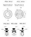
- the pupil film-formation diffractive optical device is further characterized in that parameters ⁇ i, ⁇ o and ⁇ are within the following ranges, and parameters ci and R/r are within the following ranges: 0.65 ⁇ ⁇ i ⁇ 0.75 0.8 ⁇ ⁇ o ⁇ 0.9 40 ⁇ ° ⁇ ⁇ ⁇ 50 ⁇ ° 5 % ⁇ ci ⁇ 10 % 1.5 ⁇ R / r ⁇ 1.9
- ⁇ i and ⁇ o are the inner and outer diameters of each of said two light transmissive areas
- ⁇ is the angular aperture at which said two light transmissive areas subtend the center of said pupil filter
- 1 is the radius of said pupil filter
- ci is the intensity of light having transmitted through said area of low light transmittance provided that the intensity of light having transmitted through said two light transmissive areas is 100%
- R and r are the major and minor axes of said area of low light transmittance in a substantially
- the resolving power is shown in Fig. 3(b) with the outer diameter ⁇ o of the light transmissive areas as abscissa and the optical image contrast at 130 nm as ordinate
- the stability of the optical image is shown in Fig. 3(c) with the outer diameter ⁇ o of the light transmissive areas as abscissa and the contrast range of the optical image as ordinate.
- Fig. 5(a) the resolution is shown in Fig. 5(b) with the light intensity ci as abscissa and the optical image contrast at 130 nm as ordinate, and the stability of the optical image is shown in Fig. 5(c) with the light intensity ci as abscissa and the contrast range of the optical image as ordinate.
- Fig. 6(a) shows the results of finding the optimum range for the major-to-minor axis ratio of the near-oval area 12 of low light transmittance of the dipole pupil filter.
- the major-to-minor axis ratio R/r of the near-oval area 12 of low light transmittance is increased at an increment of 0.1 from 1 to 2, where R is the major axis and r is the minor axis of the near-oval area 12.
- a known fabrication process may be applied to the fabrication of the computer-generated hologram device used for the diffractive optical device of the invention.
- a diffractive optical device having a fine-pitch relief may be fabricated by a photomask fabrication technique in combination with photolithography, wherein a transparent synthetic quartz substrate is subjected to multiple etching (for instance, two, four, or eight steps).
- Various aligners may be used, provided that the pupil filter-formation diffractive optical device of the invention can be applied to them.
- an ArF excimer laser having a wavelength of 193 nm, and a KrF excimer laser having a wavelength of 248 nm may be used as an exposure light source.
Landscapes
- Physics & Mathematics (AREA)
- General Physics & Mathematics (AREA)
- Optics & Photonics (AREA)
- Health & Medical Sciences (AREA)
- Toxicology (AREA)
- Exposure And Positioning Against Photoresist Photosensitive Materials (AREA)
- Exposure Of Semiconductors, Excluding Electron Or Ion Beam Exposure (AREA)
- Diffracting Gratings Or Hologram Optical Elements (AREA)
Applications Claiming Priority (2)
| Application Number | Priority Date | Filing Date | Title |
|---|---|---|---|
| JP2006109723A JP4957058B2 (ja) | 2006-04-12 | 2006-04-12 | 回折光学素子、および該素子を備えた露光装置 |
| PCT/JP2007/058227 WO2007119840A1 (ja) | 2006-04-12 | 2007-04-10 | 回折光学素子、および該素子を備えた露光装置 |
Publications (3)
| Publication Number | Publication Date |
|---|---|
| EP2006885A1 true EP2006885A1 (de) | 2008-12-24 |
| EP2006885A4 EP2006885A4 (de) | 2010-04-07 |
| EP2006885B1 EP2006885B1 (de) | 2014-11-26 |
Family
ID=38609599
Family Applications (1)
| Application Number | Title | Priority Date | Filing Date |
|---|---|---|---|
| EP07741663.4A Ceased EP2006885B1 (de) | 2006-04-12 | 2007-04-10 | Optisches diffraktionselement und mit diesem element ausgerüsteter ausrichter |
Country Status (5)
| Country | Link |
|---|---|
| US (1) | US8259290B2 (de) |
| EP (1) | EP2006885B1 (de) |
| JP (1) | JP4957058B2 (de) |
| TW (1) | TWI454830B (de) |
| WO (1) | WO2007119840A1 (de) |
Families Citing this family (5)
| Publication number | Priority date | Publication date | Assignee | Title |
|---|---|---|---|---|
| JP5283928B2 (ja) | 2008-02-28 | 2013-09-04 | キヤノン株式会社 | 照明光学系、露光装置及びデバイス製造方法 |
| JP2009290206A (ja) * | 2008-05-01 | 2009-12-10 | Dainippon Printing Co Ltd | 露光装置用瞳フィルタ、回折光学素子及びそれを備えた露光装置 |
| US9261793B2 (en) | 2012-09-14 | 2016-02-16 | Globalfoundries Inc. | Image optimization using pupil filters in projecting printing systems with fixed or restricted illumination angular distribution |
| CN111443576B (zh) | 2015-04-07 | 2023-04-07 | 联华电子股份有限公司 | 照明系统以及使用其形成鳍状结构的方法 |
| DE102017115262B9 (de) * | 2017-07-07 | 2021-05-27 | Carl Zeiss Smt Gmbh | Verfahren zur Charakterisierung einer Maske für die Mikrolithographie |
Family Cites Families (16)
| Publication number | Priority date | Publication date | Assignee | Title |
|---|---|---|---|---|
| DE69931690T2 (de) | 1998-04-08 | 2007-06-14 | Asml Netherlands B.V. | Lithographischer Apparat |
| US6563567B1 (en) * | 1998-12-17 | 2003-05-13 | Nikon Corporation | Method and apparatus for illuminating a surface using a projection imaging apparatus |
| JP2001174615A (ja) | 1999-04-15 | 2001-06-29 | Nikon Corp | 回折光学素子、該素子の製造方法、該素子を備える照明装置、投影露光装置、露光方法、及び光ホモジナイザー、該光ホモジナイザーの製造方法 |
| DE60024109T2 (de) * | 1999-09-21 | 2006-08-03 | The Procter & Gamble Company, Cincinnati | Gewebepflegezusammensetzungen |
| US6671035B2 (en) * | 1999-09-29 | 2003-12-30 | Asml Netherlands B.V. | Illuminator for a lithography apparatus, a lithography apparatus comprising such an illuminator, and a manufacturing method employing such a lithography apparatus |
| TW587199B (en) * | 1999-09-29 | 2004-05-11 | Asml Netherlands Bv | Lithographic method and apparatus |
| KR100343140B1 (ko) * | 1999-12-06 | 2002-07-05 | 윤종용 | 종방향 및 횡방향 패턴간의 선폭 차이에 대한 보정이가능한 노광장치 및 이에 사용되는 어퍼쳐 |
| TW546550B (en) * | 1999-12-13 | 2003-08-11 | Asml Netherlands Bv | An illuminator for a lithography apparatus, a lithography apparatus comprising such an illuminator, and a manufacturing method employing such a lithography apparatus |
| TWI285295B (en) * | 2001-02-23 | 2007-08-11 | Asml Netherlands Bv | Illumination optimization in lithography |
| KR100518586B1 (ko) | 2003-07-24 | 2005-10-04 | 삼성전자주식회사 | 회절 광학 소자와 이를 포함하는 조명계 및 이를 이용한반도체 소자 제조방법 |
| EP2278402B1 (de) * | 2003-08-26 | 2013-03-06 | Nikon Corporation | Belichtungsvorrichtung |
| JP4323903B2 (ja) * | 2003-09-12 | 2009-09-02 | キヤノン株式会社 | 照明光学系及びそれを用いた露光装置 |
| JP4684563B2 (ja) | 2004-02-26 | 2011-05-18 | キヤノン株式会社 | 露光装置及び方法 |
| JP4497968B2 (ja) * | 2004-03-18 | 2010-07-07 | キヤノン株式会社 | 照明装置、露光装置及びデバイス製造方法 |
| US7537870B2 (en) * | 2005-08-05 | 2009-05-26 | Chartered Semiconductor Manufacturing, Ltd. | Lithography process optimization and system |
| US20080297753A1 (en) * | 2007-05-31 | 2008-12-04 | Micron Technology, Inc. | Apparatus and method for defect-free microlithography |
-
2006
- 2006-04-12 JP JP2006109723A patent/JP4957058B2/ja not_active Expired - Lifetime
-
2007
- 2007-04-10 WO PCT/JP2007/058227 patent/WO2007119840A1/ja not_active Ceased
- 2007-04-10 EP EP07741663.4A patent/EP2006885B1/de not_active Ceased
- 2007-04-10 US US12/091,926 patent/US8259290B2/en active Active
- 2007-04-11 TW TW096112710A patent/TWI454830B/zh active
Also Published As
| Publication number | Publication date |
|---|---|
| TWI454830B (zh) | 2014-10-01 |
| EP2006885A4 (de) | 2010-04-07 |
| EP2006885B1 (de) | 2014-11-26 |
| JP4957058B2 (ja) | 2012-06-20 |
| US8259290B2 (en) | 2012-09-04 |
| TW200745728A (en) | 2007-12-16 |
| US20090168040A1 (en) | 2009-07-02 |
| WO2007119840A1 (ja) | 2007-10-25 |
| JP2007287719A (ja) | 2007-11-01 |
Similar Documents
| Publication | Publication Date | Title |
|---|---|---|
| EP0907111B9 (de) | Verfahren zur Herstellung einer photolithographischen Maske | |
| US6004699A (en) | Photomask used for projection exposure with phase shifted auxiliary pattern | |
| KR100714480B1 (ko) | 포토마스크의 테스트 패턴 이미지로부터 인쇄된 테스트피쳐들을 이용하는 포토리소그래피 공정에 있어서 초점변화를 측정하는 시스템 및 방법 | |
| US7032209B2 (en) | Mask pattern and method for forming resist pattern using mask pattern thereof | |
| US6379868B1 (en) | Lithographic process for device fabrication using dark-field illumination | |
| US7910266B2 (en) | Pattern forming method and mask | |
| KR20030014760A (ko) | 기판을 제조하는 리소그래피 방법 및 장치 | |
| JPH10133356A (ja) | フォトマスクおよびパターン形成方法 | |
| US20010036604A1 (en) | Multiple exposure method | |
| JP2002075823A (ja) | 半導体装置のパターン形成方法、フォトマスクのパターン設計方法、フォトマスクの製造方法およびフォトマスク | |
| JP5143356B2 (ja) | 二重露光技術を用いた二重露光方法及びこの二重露光方法のためのフォトマスク | |
| EP2006885B1 (de) | Optisches diffraktionselement und mit diesem element ausgerüsteter ausrichter | |
| US6377337B1 (en) | Projection exposure apparatus | |
| JP4495663B2 (ja) | サブ分解能アシストフューチャとしてグレーバーを使用する光近接補正方法 | |
| US7846625B2 (en) | Phase shift mask | |
| US5840448A (en) | Phase shifting mask having a phase shift that minimizes critical dimension sensitivity to manufacturing and process variance | |
| US5663785A (en) | Diffraction pupil filler modified illuminator for annular pupil fills | |
| JPH10233361A (ja) | 露光方法と露光用マスク | |
| US20060197933A1 (en) | Exposure apparatus | |
| US6480263B1 (en) | Apparatus and method for phase shift photomasking | |
| JP2001100391A (ja) | 半導体露光用レティクル、半導体露光用レティクルの製造方法および半導体装置 | |
| JPH11143048A (ja) | 位相シフトマスク | |
| JP4011896B2 (ja) | 露光方法 | |
| JP2003131357A (ja) | 投影露光用マスク | |
| JP2000021756A (ja) | パターン形成方法及び露光装置 |
Legal Events
| Date | Code | Title | Description |
|---|---|---|---|
| PUAI | Public reference made under article 153(3) epc to a published international application that has entered the european phase |
Free format text: ORIGINAL CODE: 0009012 |
|
| 17P | Request for examination filed |
Effective date: 20080103 |
|
| AK | Designated contracting states |
Kind code of ref document: A1 Designated state(s): DE NL |
|
| RBV | Designated contracting states (corrected) |
Designated state(s): DE NL |
|
| A4 | Supplementary search report drawn up and despatched |
Effective date: 20100305 |
|
| 17Q | First examination report despatched |
Effective date: 20100623 |
|
| DAX | Request for extension of the european patent (deleted) | ||
| GRAP | Despatch of communication of intention to grant a patent |
Free format text: ORIGINAL CODE: EPIDOSNIGR1 |
|
| INTG | Intention to grant announced |
Effective date: 20140710 |
|
| GRAS | Grant fee paid |
Free format text: ORIGINAL CODE: EPIDOSNIGR3 |
|
| GRAA | (expected) grant |
Free format text: ORIGINAL CODE: 0009210 |
|
| AK | Designated contracting states |
Kind code of ref document: B1 Designated state(s): DE NL |
|
| RAP1 | Party data changed (applicant data changed or rights of an application transferred) |
Owner name: DAI NIPPON PRINTING CO., LTD. |
|
| REG | Reference to a national code |
Ref country code: DE Ref legal event code: R096 Ref document number: 602007039426 Country of ref document: DE Effective date: 20141231 |
|
| REG | Reference to a national code |
Ref country code: NL Ref legal event code: T3 |
|
| REG | Reference to a national code |
Ref country code: DE Ref legal event code: R097 Ref document number: 602007039426 Country of ref document: DE |
|
| PLBE | No opposition filed within time limit |
Free format text: ORIGINAL CODE: 0009261 |
|
| STAA | Information on the status of an ep patent application or granted ep patent |
Free format text: STATUS: NO OPPOSITION FILED WITHIN TIME LIMIT |
|
| 26N | No opposition filed |
Effective date: 20150827 |
|
| PGFP | Annual fee paid to national office [announced via postgrant information from national office to epo] |
Ref country code: DE Payment date: 20200420 Year of fee payment: 14 Ref country code: NL Payment date: 20200427 Year of fee payment: 14 |
|
| REG | Reference to a national code |
Ref country code: DE Ref legal event code: R119 Ref document number: 602007039426 Country of ref document: DE |
|
| REG | Reference to a national code |
Ref country code: NL Ref legal event code: MM Effective date: 20210501 |
|
| PG25 | Lapsed in a contracting state [announced via postgrant information from national office to epo] |
Ref country code: DE Free format text: LAPSE BECAUSE OF NON-PAYMENT OF DUE FEES Effective date: 20211103 |
|
| PG25 | Lapsed in a contracting state [announced via postgrant information from national office to epo] |
Ref country code: NL Free format text: LAPSE BECAUSE OF NON-PAYMENT OF DUE FEES Effective date: 20210501 |