EP2006933B1 - Affichage électroluminescent organique et son procédé de fabrication - Google Patents
Affichage électroluminescent organique et son procédé de fabrication Download PDFInfo
- Publication number
- EP2006933B1 EP2006933B1 EP08252109.7A EP08252109A EP2006933B1 EP 2006933 B1 EP2006933 B1 EP 2006933B1 EP 08252109 A EP08252109 A EP 08252109A EP 2006933 B1 EP2006933 B1 EP 2006933B1
- Authority
- EP
- European Patent Office
- Prior art keywords
- light emitting
- organic light
- emitting display
- electrodes
- substrate
- Prior art date
- Legal status (The legal status is an assumption and is not a legal conclusion. Google has not performed a legal analysis and makes no representation as to the accuracy of the status listed.)
- Not-in-force
Links
Images



Classifications
-
- H—ELECTRICITY
- H05—ELECTRIC TECHNIQUES NOT OTHERWISE PROVIDED FOR
- H05B—ELECTRIC HEATING; ELECTRIC LIGHT SOURCES NOT OTHERWISE PROVIDED FOR; CIRCUIT ARRANGEMENTS FOR ELECTRIC LIGHT SOURCES, IN GENERAL
- H05B33/00—Electroluminescent light sources
- H05B33/02—Details
- H05B33/04—Sealing arrangements, e.g. against humidity
-
- H—ELECTRICITY
- H10—SEMICONDUCTOR DEVICES; ELECTRIC SOLID-STATE DEVICES NOT OTHERWISE PROVIDED FOR
- H10K—ORGANIC ELECTRIC SOLID-STATE DEVICES
- H10K59/00—Integrated devices, or assemblies of multiple devices, comprising at least one organic light-emitting element covered by group H10K50/00
- H10K59/80—Constructional details
- H10K59/87—Passivation; Containers; Encapsulations
- H10K59/871—Self-supporting sealing arrangements
- H10K59/8723—Vertical spacers, e.g. arranged between the sealing arrangement and the OLED
-
- H—ELECTRICITY
- H05—ELECTRIC TECHNIQUES NOT OTHERWISE PROVIDED FOR
- H05B—ELECTRIC HEATING; ELECTRIC LIGHT SOURCES NOT OTHERWISE PROVIDED FOR; CIRCUIT ARRANGEMENTS FOR ELECTRIC LIGHT SOURCES, IN GENERAL
- H05B33/00—Electroluminescent light sources
- H05B33/12—Light sources with substantially two-dimensional [2D] radiating surfaces
- H05B33/22—Light sources with substantially two-dimensional [2D] radiating surfaces characterised by the chemical or physical composition or the arrangement of auxiliary dielectric or reflective layers
-
- H—ELECTRICITY
- H10—SEMICONDUCTOR DEVICES; ELECTRIC SOLID-STATE DEVICES NOT OTHERWISE PROVIDED FOR
- H10K—ORGANIC ELECTRIC SOLID-STATE DEVICES
- H10K50/00—Organic light-emitting devices
- H10K50/80—Constructional details
- H10K50/84—Passivation; Containers; Encapsulations
- H10K50/842—Containers
- H10K50/8428—Vertical spacers, e.g. arranged between the sealing arrangement and the OLED
-
- H—ELECTRICITY
- H10—SEMICONDUCTOR DEVICES; ELECTRIC SOLID-STATE DEVICES NOT OTHERWISE PROVIDED FOR
- H10K—ORGANIC ELECTRIC SOLID-STATE DEVICES
- H10K50/00—Organic light-emitting devices
- H10K50/80—Constructional details
- H10K50/84—Passivation; Containers; Encapsulations
- H10K50/844—Encapsulations
- H10K50/8445—Encapsulations multilayered coatings having a repetitive structure, e.g. having multiple organic-inorganic bilayers
-
- H—ELECTRICITY
- H10—SEMICONDUCTOR DEVICES; ELECTRIC SOLID-STATE DEVICES NOT OTHERWISE PROVIDED FOR
- H10K—ORGANIC ELECTRIC SOLID-STATE DEVICES
- H10K50/00—Organic light-emitting devices
- H10K50/80—Constructional details
- H10K50/84—Passivation; Containers; Encapsulations
- H10K50/846—Passivation; Containers; Encapsulations comprising getter material or desiccants
-
- H—ELECTRICITY
- H10—SEMICONDUCTOR DEVICES; ELECTRIC SOLID-STATE DEVICES NOT OTHERWISE PROVIDED FOR
- H10K—ORGANIC ELECTRIC SOLID-STATE DEVICES
- H10K59/00—Integrated devices, or assemblies of multiple devices, comprising at least one organic light-emitting element covered by group H10K50/00
- H10K59/80—Constructional details
- H10K59/87—Passivation; Containers; Encapsulations
- H10K59/873—Encapsulations
- H10K59/8731—Encapsulations multilayered coatings having a repetitive structure, e.g. having multiple organic-inorganic bilayers
-
- H—ELECTRICITY
- H10—SEMICONDUCTOR DEVICES; ELECTRIC SOLID-STATE DEVICES NOT OTHERWISE PROVIDED FOR
- H10K—ORGANIC ELECTRIC SOLID-STATE DEVICES
- H10K59/00—Integrated devices, or assemblies of multiple devices, comprising at least one organic light-emitting element covered by group H10K50/00
- H10K59/80—Constructional details
- H10K59/87—Passivation; Containers; Encapsulations
- H10K59/874—Passivation; Containers; Encapsulations including getter material or desiccant
-
- H—ELECTRICITY
- H10—SEMICONDUCTOR DEVICES; ELECTRIC SOLID-STATE DEVICES NOT OTHERWISE PROVIDED FOR
- H10K—ORGANIC ELECTRIC SOLID-STATE DEVICES
- H10K59/00—Integrated devices, or assemblies of multiple devices, comprising at least one organic light-emitting element covered by group H10K50/00
- H10K59/10—OLED displays
- H10K59/12—Active-matrix OLED [AMOLED] displays
- H10K59/122—Pixel-defining structures or layers, e.g. banks
-
- H—ELECTRICITY
- H10—SEMICONDUCTOR DEVICES; ELECTRIC SOLID-STATE DEVICES NOT OTHERWISE PROVIDED FOR
- H10K—ORGANIC ELECTRIC SOLID-STATE DEVICES
- H10K71/00—Manufacture or treatment specially adapted for the organic devices covered by this subclass
- H10K71/10—Deposition of organic active material
- H10K71/18—Deposition of organic active material using non-liquid printing techniques, e.g. thermal transfer printing from a donor sheet
Definitions
- aspects of the present invention relate to an organic light emitting display, and a method of manufacturing the same, and more particularly, to an organic light emitting display including spacers, and a method of manufacturing the same.
- An organic light emitting display is a self-emission type display that electrically excites phosphorous organic compounds to generate light.
- An organic light emitting display can be driven with a low voltage, can be made small and slim, can have a wide viewing angle, and can have a high response speed. Therefore, organic light emitting displays are spotlighted as next generation displays, and in particular, displays for mobile applications.
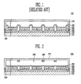
- FIG. 1 is a cross-sectional view illustrating a conventional organic light emitting display 100.
- the organic light emitting display 100 includes a substrate 110 including thin film transistors (TFTs) 120, organic light emitting diodes (OLEDs), and an encapsulating unit 170 that encapsulates the OLEDs.
- the OLEDs include: first electrodes 130 that are electrically connected to the TFTs 120; a pixel defining layer 140 formed around the first electrodes 130; organic thin layers 150 formed on the first electrodes 130; and second electrodes 160 formed on the organic thin layers 150.
- US2006192487 discloses a display device includes a first substrate, light emitting elements formed over the first substrate, a second substrate facing the first substrate, and a sealing member between the first and the second substrate to combine them.
- the sealing member is patterned to expose the light emitting elements.
- EP1670081 discloses an organic light emitting display device and a method of fabricating the same.
- a dummy pattern (328,336,356) is formed in an emission region (I) to increase the step height of the emission region (I) by an electrode material while a thin film transistor is fabricated, so that a distance between a pixel electrode and a donor film (T2) is decreased during fabrication of an organic layer.
- US 2006/0290276 discloses an OLED having spacer elements formed on the internal surface of an encapsulation substrate, wherein it is disclosed that these may be formed from barium oxide or metal oxides.
- the present invention sets out to provide an organic light emitting display that protects organic light emitting diodes (OLEDs) from oxygen and/or moisture. Aspects of the invention also set out to improve the mechanical strength of the organic light emitting display.
- OLEDs organic light emitting diodes
- the invention provides an organic light emitting display device as set out in Claim 1. Preferred features of this aspect of the invention are set out in Claims 2 to 10.
- the invention also provides a method of fabricating an organic light emitting display as set out in Claim 11. Preferred features of this aspect of the invention are set out in Claims 12 to 14.
- FIG. 1 is a cross-sectional view illustrating an organic light emitting display
- FIG. 2 is a cross-sectional view illustrating an organic light emitting display, according to a first embodiment of the present invention
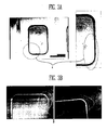
- FIGS. 3A and 3B are micrographs illustrating the surface of an organic thin layer
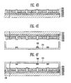
- FIGS. 4A to 4F illustrate a method of manufacturing the organic light emitting display, according to the first embodiment of the present invention
- FIG. 5 is a cross-sectional view of an organic light emitting display, according to a second embodiment of the present invention.
- FIG. 6 is a cross-sectional view of an organic light emitting display, according to a third embodiment of the present invention.
- FIG. 7 is a cross-sectional view of an organic light emitting display, according to a fourth embodiment of the present invention.
- FIG. 8 is a plan view illustrating spacers, according to an embodiment of the present invention.
- the spacers 280 are formed on the internal surface of the encapsulating unit 270, facing a portion of the pixel defining layer 240.
- the pixel defining layer 240 separates the OLEDs 205 from each other, and can assist the operation of the spacers 280.
- the spacers 280 allow for a reduction in the thickness of the pixel defining layer 240.
- the spacers 280 allow for the thickness of the pixel defining layer 240 to be reduced, so that the organic thin layers 250 can be uniformly formed using the LITI method or the mask method. That is, the thickness of the pixel defining layer 240 is decreased, to reduce the distance between the mask (not shown) provided on the pixel defining layer 240, or the donor film 300 ( FIG. 4B ) and the first electrodes 230. As a result, the organic thin layers 250 can be correctly formed on the first electrodes 230.
- the encapsulating unit 270 faces the substrate 210, and is separated from the second electrodes 260.
- the encapsulating unit 270 can be formed of an encapsulating substrate, or an encapsulating thin layer.
- the encapsulating unit 270 can be shaped as a rectangular prism having an open bottom.
- the encapsulating substrate 270 can be attached to the substrate 210, by a sealing material 290 applied to the edge of the open bottom of the encapsulating substrate 270.
- the spacers 280 have a thickness of 3 to 5 ⁇ m. When the thickness of the spacers 280 is less than about 3 ⁇ m, the organic thin layers 250 can be damaged, if the encapsulating unit 270 is forced toward the substrate 210. When the thickness of the spacers 280 is more that about 5 ⁇ m, the thickness of the organic light emitting display 200 may be unnecessarily increased.
- FIGS. 3A and 3B are micrographs illustrating the surface of the organic thin layer 250.
- FIG. 3A illustrates the case in which an organic thin layer is formed by the LITI method, and the thickness of pixel defining layer is 1.5 ⁇ m. As shown, the organic thin layer in region A is not uniformly formed.
- FIG. 3B illustrates the case in which an organic thin layer is formed by the LITI method, and the thickness of pixel defining layer is 0.2 ⁇ m. As shown, the organic thin layer in region "B" is uniformly formed.
- the donor film 300 is laminated on the substrate 210.
- the lamination is performed so that the donor film 300 is well attached to the substrate 210.
- the donor film 300 can be laminated onto the accepter substrate 210, using a roller.
- the organic thin layers 250 can be uniformly formed on the first electrodes 230.
- a laser beam 350 is radiated onto portions of the donor film 300, corresponding to where the organic thin layers 250 are to be formed.
- the second electrodes 260 are formed on the pixel defining layer 240 and the organic thin layers 250.
- the glass frits can include at least one selected from the group consisting of K 2 O, Fe 2 O 3 , Sb 2 O 3 , ZnO, P 2 O 5 , V 2 O 5 , TiO 2 , Al 2 O 3 , B 2 O 3 , WO 3 , SnO, and PbO.
- the encapsulating unit 670 faces the substrate 210, and is separated from the second electrodes 660, by the protecting layer 665.
- the encapsulating unit 670 can be formed of an encapsulating thin layer.
- the protecting layer 665 planarizes a contact surface of the OLEDs 205 and improves the bonding of the encapsulating unit thereto.
- the protecting layer 665 can be formed of one selected from the group consisting of an inorganic material, an oxide, a nitride, and an organic material, such as LiF, SiO 2 , SixNy, SiOxNy, and Al 2 O 3 .
Landscapes
- Chemical & Material Sciences (AREA)
- Inorganic Chemistry (AREA)
- Physics & Mathematics (AREA)
- Optics & Photonics (AREA)
- Electroluminescent Light Sources (AREA)
- Devices For Indicating Variable Information By Combining Individual Elements (AREA)
Claims (14)
- Affichage électroluminescent organique comprenant :un substrat (210) ;des transistors en couches minces (TFT) disposées sur le substrat (210) ;des diodes électroluminescentes organiques (OLED) disposées sur les TFT, les OLED comprenant :des premières électrodes (230) reliées électriquement aux TFT,une couche de définition de pixels (240) disposée autour des premières électrodes (230),des couches organiques (250) formées sur les premières électrodes (230), etdes deuxièmes électrodes (260) formées sur les couches organiques (250) ;une unité d'encapsulation (270) disposée sur le substrat (210), permettant d'encapsuler les OLED ; etune entretoise (280) fabriquée à partir d'un matériau absorbant l'humidité, disposée sur l'unité d'encapsulation (270), faisant face à la couche de définition de pixels (240) ;dans lequel l'entretoise (280) est formée sur une surface interne de l'unité d'encapsulation (270) à une position correspondant à celle de la couche de définition de pixels (240), et l'entretoise (280) est séparée des deuxièmes électrodes (260) ; etdans lequel la couche de définition de pixels (240) a une épaisseur de 0,05 à 0,3 µm et l'entretoise (280) a une épaisseur de 3 à 5 µm.
- Affichage électroluminescent organique selon la revendication 1, dans lequel le matériau absorbant l'humidité comprend au moins l'un de : oxyde de baryum, oxyde de potassium, oxyde de calcium, oxyde d'aluminium, sulfate de lithium, hydrosulfite de sodium, sulfate de calcium, sulfate de magnésium, sulfate de cobalt, sulfate de gallium, sulfate de titane, chlorure de calcium, nitrate de calcium tétrahydraté, oxyde de magnésium, oxyde de métal alcalin, oxyde de métal alcalino-terreux, halogénure de métal, un chlorure de métal, un perchlorate de métal, pentoxyde de phosphore et sulfate de nickel.
- Affichage électroluminescent organique selon l'une quelconque des revendications précédentes, comprenant en outre une pluralité d'entretoises (280).
- Affichage électroluminescent organique selon l'une quelconque des revendications précédentes, dans lequel l'unité d'encapsulation (270) se présente sous la forme d'un prisme rectangulaire ayant une extrémité ouverte.
- Affichage électroluminescent organique selon l'une quelconque des revendications 1 à 3, dans lequel l'unité d'encapsulation comprend une couche stratifiée comprenant au moins une couche organique et au moins une couche inorganique.
- Affichage électroluminescent organique selon la revendication 4, comprenant en outre un produit d'étanchéité permettant de fixer le substrat à l'unité d'encapsulation, disposé entre le substrat et l'unité d'encapsulation (270).
- Affichage électroluminescent organique selon la revendication 6, dans lequel le produit d'étanchéité est un produit d'étanchéité inorganique.
- Affichage électroluminescent organique selon la revendication 1, dans lequel l'entretoise (280) est disposée sur l'unité d'encapsulation (270) selon un motif en grille.
- Affichage électroluminescent organique selon la revendication 3, dans lequel les entretoises sont disposées sur l'unité d'encapsulation (270) selon un motif en damier, ou par groupes de 4.
- Affichage électroluminescent organique selon l'une quelconque des revendications précédentes, comprenant en outre une couche de protection disposée entre les deuxièmes électrodes (260) et l'unité d'encapsulation (270).
- Procédé de fabrication d'un affichage électroluminescent organique comprenant :la formation de premières électrodes (230) sur les transistors en couches minces (TFT) d'un substrat (210) ;la formation d'une couche de définition de pixels (240) autour des premières électrodes (230), la couche de définition de pixels (240) ayant une épaisseur de 0,05 à 0,3 µm ;la formation de couches organiques (250) sur les premières électrodes (230) par imagerie thermique induite par laser (LITI) ;la formation de deuxièmes électrodes (260) sur les couches organiques (250) ;la formation d'une entretoise (280) comprenant un matériau absorbant l'humidité et ayant une épaisseur de 3 à 5 µm, sur une unité d'encapsulation (270) ; etla fixation de l'unité d'encapsulation (270) au substrat (210), dans lequel,l'entretoise (280) est disposée de manière à faire face à au moins une partie de la couche de définition de pixels (240), et est séparée des deuxièmes électrodes (260).
- Procédé selon la revendication 11, dans lequel l'entretoise (280) est formée par l'un d'un procédé de dépôt, d'un procédé d'impression d'écran et d'un procédé de pulvérisation.
- Procédé selon la revendication 11 ou 12, dans lequel l'entretoise (280) est formée en utilisant un masque perforé.
- Procédé selon l'une quelconque des revendications 11 à 13, utilisé pour fabriquer un affichage électroluminescent organique tel que défini dans l'une des revendications 1 à 10.
Applications Claiming Priority (1)
| Application Number | Priority Date | Filing Date | Title |
|---|---|---|---|
| KR1020070059726A KR100889677B1 (ko) | 2007-06-19 | 2007-06-19 | 유기 전계 발광표시장치 및 그의 제조방법 |
Publications (3)
| Publication Number | Publication Date |
|---|---|
| EP2006933A2 EP2006933A2 (fr) | 2008-12-24 |
| EP2006933A3 EP2006933A3 (fr) | 2011-03-02 |
| EP2006933B1 true EP2006933B1 (fr) | 2014-10-01 |
Family
ID=39769503
Family Applications (1)
| Application Number | Title | Priority Date | Filing Date |
|---|---|---|---|
| EP08252109.7A Not-in-force EP2006933B1 (fr) | 2007-06-19 | 2008-06-19 | Affichage électroluminescent organique et son procédé de fabrication |
Country Status (5)
| Country | Link |
|---|---|
| US (1) | US8169140B2 (fr) |
| EP (1) | EP2006933B1 (fr) |
| JP (1) | JP2009004359A (fr) |
| KR (1) | KR100889677B1 (fr) |
| CN (1) | CN101330095A (fr) |
Families Citing this family (48)
| Publication number | Priority date | Publication date | Assignee | Title |
|---|---|---|---|---|
| KR100833775B1 (ko) * | 2007-08-03 | 2008-05-29 | 삼성에스디아이 주식회사 | 유기 전계 발광 표시 장치 |
| KR20100097513A (ko) * | 2009-02-26 | 2010-09-03 | 삼성모바일디스플레이주식회사 | 유기 발광 표시 장치 |
| US20110163663A1 (en) * | 2010-01-07 | 2011-07-07 | Samsung Mobile Display Co., Ltd. | Organic Light Emitting Display Device and Method of Making the Same |
| KR101084248B1 (ko) * | 2010-01-20 | 2011-11-16 | 삼성모바일디스플레이주식회사 | 유기 발광 표시 장치 |
| KR101202352B1 (ko) * | 2010-07-19 | 2012-11-16 | 삼성디스플레이 주식회사 | 유기 발광 표시 장치 및 이의 제조 방법 |
| GB2484713A (en) | 2010-10-21 | 2012-04-25 | Optovate Ltd | Illumination apparatus |
| KR20120119089A (ko) * | 2011-04-20 | 2012-10-30 | 삼성디스플레이 주식회사 | 유기발광표시장치 제조방법 |
| KR20130006936A (ko) * | 2011-06-27 | 2013-01-18 | 삼성디스플레이 주식회사 | 유기 발광 표시 장치 |
| CN102709487B (zh) * | 2011-10-17 | 2015-06-17 | 京东方科技集团股份有限公司 | 一种有机发光显示面板及其制造方法 |
| KR101984873B1 (ko) | 2012-05-07 | 2019-06-03 | 삼성디스플레이 주식회사 | 표시 장치 및 그 제조 방법 |
| KR101703985B1 (ko) | 2012-08-22 | 2017-02-08 | 삼성디스플레이 주식회사 | 액정 표시 장치 및 그 제조 방법 |
| KR20140031003A (ko) * | 2012-09-04 | 2014-03-12 | 삼성디스플레이 주식회사 | 유기 발광 표시 장치 및 그 제조 방법 |
| KR20140048459A (ko) | 2012-10-15 | 2014-04-24 | 삼성디스플레이 주식회사 | 액정 표시 장치 및 그 제조 방법 |
| KR20140075467A (ko) * | 2012-12-11 | 2014-06-19 | 삼성디스플레이 주식회사 | 디스플레이 장치 및 디스플레이 장치의 제조방법 |
| KR20150000641A (ko) * | 2013-06-25 | 2015-01-05 | 삼성디스플레이 주식회사 | 컬러 필터 기판 |
| KR20150030105A (ko) | 2013-09-11 | 2015-03-19 | 삼성디스플레이 주식회사 | 액정 표시 장치 및 그 제조 방법 |
| KR102088203B1 (ko) * | 2013-10-01 | 2020-03-12 | 엘지디스플레이 주식회사 | 유기발광 표시장치 및 이의 제조방법 |
| CN104733645B (zh) * | 2013-12-24 | 2018-08-07 | 昆山国显光电有限公司 | 一种oled器件的封装方法及一种oled器件 |
| CN103972267B (zh) * | 2014-04-16 | 2016-09-14 | 京东方科技集团股份有限公司 | 一种有机发光显示装置 |
| FR3023979B1 (fr) * | 2014-07-17 | 2016-07-29 | Saint Gobain | Support electroconducteur pour oled, oled l'incorporant, et sa fabrication. |
| US20170271621A1 (en) * | 2014-08-22 | 2017-09-21 | Oledworks Gmbh | Light-emitting device |
| CN104617234A (zh) * | 2015-02-13 | 2015-05-13 | 京东方科技集团股份有限公司 | 隔垫物、有机电致发光显示面板、制作方法及显示装置 |
| CN105826357A (zh) * | 2016-05-16 | 2016-08-03 | 京东方科技集团股份有限公司 | 一种显示基板及oled显示装置 |
| CN106058076B (zh) * | 2016-08-19 | 2018-05-18 | 京东方科技集团股份有限公司 | 一种显示面板、显示装置及制作方法 |
| CN106328825B (zh) * | 2016-10-31 | 2019-01-15 | 武汉华星光电技术有限公司 | Oled显示器 |
| KR102711102B1 (ko) * | 2016-11-15 | 2024-09-27 | 삼성디스플레이 주식회사 | 유기 발광 표시 장치 및 그 제조 방법 |
| CN108630829B (zh) * | 2017-03-17 | 2019-11-08 | 京东方科技集团股份有限公司 | 显示面板的制作方法、显示面板及显示装置 |
| GB201705364D0 (en) | 2017-04-03 | 2017-05-17 | Optovate Ltd | Illumination apparatus |
| GB201705365D0 (en) | 2017-04-03 | 2017-05-17 | Optovate Ltd | Illumination apparatus |
| GB201718307D0 (en) | 2017-11-05 | 2017-12-20 | Optovate Ltd | Display apparatus |
| KR101874430B1 (ko) * | 2018-01-10 | 2018-07-06 | 삼성디스플레이 주식회사 | 유기발광표시장치 및 그 제조방법 |
| GB201800574D0 (en) | 2018-01-14 | 2018-02-28 | Optovate Ltd | Illumination apparatus |
| GB201803767D0 (en) | 2018-03-09 | 2018-04-25 | Optovate Ltd | Illumination apparatus |
| GB201807747D0 (en) | 2018-05-13 | 2018-06-27 | Optovate Ltd | Colour micro-LED display apparatus |
| CN109638045B (zh) * | 2018-12-07 | 2020-06-16 | 武汉华星光电半导体显示技术有限公司 | 显示单元、显示单元的制作方法和有机发光二极管显示器 |
| CN111192972A (zh) * | 2019-03-18 | 2020-05-22 | 广东聚华印刷显示技术有限公司 | 薄膜封装结构及其制备方法和显示装置 |
| US10902912B2 (en) | 2019-06-12 | 2021-01-26 | International Business Machines Corporation | Electrochemical switching device with protective encapsulation |
| TWI912252B (zh) | 2019-07-02 | 2026-01-21 | 美商瑞爾D斯帕克有限責任公司 | 定向顯示設備 |
| EP4018236A4 (fr) | 2019-08-23 | 2023-09-13 | RealD Spark, LLC | Appareil d'éclairage directionnel et affichage de confidentialité |
| KR102800511B1 (ko) * | 2019-09-03 | 2025-04-28 | 삼성디스플레이 주식회사 | 표시 장치 |
| US11163101B2 (en) | 2019-09-11 | 2021-11-02 | Reald Spark, Llc | Switchable illumination apparatus and privacy display |
| CN114730044B (zh) | 2019-09-11 | 2025-03-21 | 瑞尔D斯帕克有限责任公司 | 定向照明设备和隐私显示器 |
| JP7548655B2 (ja) | 2019-10-03 | 2024-09-10 | リアルディー スパーク エルエルシー | 受動光学ナノ構造を備える照明装置 |
| KR102937412B1 (ko) | 2019-10-03 | 2026-03-12 | 리얼디 스파크, 엘엘씨 | 수동형 광학 나노구조를 포함하는 조명 장치 |
| WO2021131009A1 (fr) * | 2019-12-27 | 2021-07-01 | シャープ株式会社 | Procédé de fabrication de dispositif d'affichage, et dispositif d'affichage |
| EP4107580A4 (fr) | 2020-02-20 | 2024-03-20 | RealD Spark, LLC | Appareil d'éclairage et d'affichage |
| KR20220087298A (ko) | 2020-12-17 | 2022-06-24 | 삼성전자주식회사 | 반도체 발광 소자 및 그 제조 방법 |
| WO2022271582A1 (fr) | 2021-06-22 | 2022-12-29 | Reald Spark, Llc | Appareil d'éclairage |
Citations (1)
| Publication number | Priority date | Publication date | Assignee | Title |
|---|---|---|---|---|
| US20060290276A1 (en) * | 2005-06-22 | 2006-12-28 | Eastman Kodak Company | OLED device having spacers |
Family Cites Families (22)
| Publication number | Priority date | Publication date | Assignee | Title |
|---|---|---|---|---|
| US53719A (en) * | 1866-04-03 | Improvement in scissors | ||
| US192487A (en) * | 1877-06-26 | Improvement in apparatus for automatically reducing or regulating fluid-pressure | ||
| US6195142B1 (en) * | 1995-12-28 | 2001-02-27 | Matsushita Electrical Industrial Company, Ltd. | Organic electroluminescence element, its manufacturing method, and display device using organic electroluminescence element |
| US7495390B2 (en) * | 2000-12-23 | 2009-02-24 | Lg Display Co., Ltd. | Electro-luminescence device with improved thermal conductivity |
| JP2002231441A (ja) * | 2001-01-31 | 2002-08-16 | Nippon Seiki Co Ltd | 有機elパネル |
| TW548860B (en) * | 2001-06-20 | 2003-08-21 | Semiconductor Energy Lab | Light emitting device and method of manufacturing the same |
| US6963169B2 (en) | 2001-11-13 | 2005-11-08 | Kuan-Chang Peng | Organic electro-luminescence device |
| JP3705264B2 (ja) * | 2001-12-18 | 2005-10-12 | セイコーエプソン株式会社 | 表示装置及び電子機器 |
| JP3975779B2 (ja) | 2002-03-01 | 2007-09-12 | 株式会社日立製作所 | 有機エレクトロルミネッセンス装置およびその製造方法 |
| JP2005044613A (ja) | 2003-07-28 | 2005-02-17 | Seiko Epson Corp | 発光装置の製造方法および発光装置 |
| KR100611145B1 (ko) | 2003-11-25 | 2006-08-09 | 삼성에스디아이 주식회사 | 풀칼라 유기 전계 발광 소자용 도너 필름, 도너 필름의제조 방법 및 이 도너 필름을 사용한 풀칼라 유기 전계발광 소자 |
| JP2005166315A (ja) * | 2003-11-28 | 2005-06-23 | Toshiba Matsushita Display Technology Co Ltd | 有機el表示装置 |
| US7792489B2 (en) * | 2003-12-26 | 2010-09-07 | Semiconductor Energy Laboratory Co., Ltd. | Light emitting device, electronic appliance, and method for manufacturing light emitting device |
| KR100635575B1 (ko) * | 2004-11-17 | 2006-10-17 | 삼성에스디아이 주식회사 | 풀 칼라 유기 전계 발광 표시 소자 및 그 제조방법 |
| KR100700642B1 (ko) | 2004-12-13 | 2007-03-27 | 삼성에스디아이 주식회사 | 유기전계발광표시소자 및 그 제조방법 |
| KR20060094685A (ko) | 2005-02-25 | 2006-08-30 | 삼성전자주식회사 | 표시 장치 및 이의 제조 방법 |
| JP2006269257A (ja) * | 2005-03-24 | 2006-10-05 | Seiko Epson Corp | 電気光学装置、電気光学装置の製造方法、電子機器 |
| KR101149935B1 (ko) | 2005-03-25 | 2012-06-01 | 엘지디스플레이 주식회사 | 유기전계발광소자 |
| US7906906B2 (en) * | 2005-03-25 | 2011-03-15 | Lg Display Co., Ltd. | Light emitting device having spacer for protecting light emission unit from moisture absorbent |
| KR101128462B1 (ko) | 2005-03-25 | 2012-03-26 | 엘지디스플레이 주식회사 | 유기전계발광소자 |
| US7459850B2 (en) | 2005-06-22 | 2008-12-02 | Eastman Kodak Company | OLED device having spacers |
| KR100879857B1 (ko) * | 2007-07-04 | 2009-01-22 | 삼성모바일디스플레이주식회사 | 유기전계발광 표시장치 및 그 제조방법 |
-
2007
- 2007-06-19 KR KR1020070059726A patent/KR100889677B1/ko not_active Expired - Fee Related
-
2008
- 2008-03-26 JP JP2008079891A patent/JP2009004359A/ja active Pending
- 2008-06-17 US US12/140,614 patent/US8169140B2/en not_active Expired - Fee Related
- 2008-06-18 CN CNA2008101102153A patent/CN101330095A/zh active Pending
- 2008-06-19 EP EP08252109.7A patent/EP2006933B1/fr not_active Not-in-force
Patent Citations (1)
| Publication number | Priority date | Publication date | Assignee | Title |
|---|---|---|---|---|
| US20060290276A1 (en) * | 2005-06-22 | 2006-12-28 | Eastman Kodak Company | OLED device having spacers |
Also Published As
| Publication number | Publication date |
|---|---|
| CN101330095A (zh) | 2008-12-24 |
| US8169140B2 (en) | 2012-05-01 |
| US20080315755A1 (en) | 2008-12-25 |
| JP2009004359A (ja) | 2009-01-08 |
| KR100889677B1 (ko) | 2009-03-19 |
| KR20080111593A (ko) | 2008-12-24 |
| EP2006933A2 (fr) | 2008-12-24 |
| EP2006933A3 (fr) | 2011-03-02 |
Similar Documents
| Publication | Publication Date | Title |
|---|---|---|
| US8169140B2 (en) | Organic light emitting display including spacer and method of manufacturing the same | |
| KR102124040B1 (ko) | 박막 증착용 마스크, 이의 제조 방법, 및 이를 이용한 유기 발광 표시 장치의 제조 방법 | |
| KR101814775B1 (ko) | 유기발광다이오드 표시장치의 제조방법 | |
| KR101368725B1 (ko) | 유기 전계 발광 표시장치 및 그 제조방법 | |
| US11508933B2 (en) | Display panel and display device | |
| US6774392B2 (en) | Organic light emitting diode and method for producing the same | |
| CN113838994A (zh) | 显示面板、柔性显示屏和电子设备及显示面板的制备方法 | |
| KR20150043142A (ko) | 유기발광표시장치 및 그 제조방법 | |
| US9748515B2 (en) | Organic light-emitting diode display and method of manufacturing the same including a sealant with a plurality of openings and islands formed within the openings | |
| CN103682143A (zh) | 有机发光显示装置及其制造方法 | |
| US8455897B2 (en) | Organic light-emitting display apparatus and method of manufacturing the same | |
| US8439719B2 (en) | Method of encapsulating organic light emitting display device | |
| CN107331692B (zh) | Oled显示面板及其制作方法 | |
| CN109644531B (zh) | 有机el显示装置及其制造方法 | |
| CN110620133A (zh) | 一种透明显示面板及其制备方法和显示装置 | |
| US9825251B2 (en) | Display apparatus comprising a seal portion having two different thicknesses | |
| KR20160032970A (ko) | 유기 발광 표시 장치 및 유기 발광 표시 장치 제조 방법 | |
| CN110660833B (zh) | 电致发光显示器件及其制备方法 | |
| CN108666437B (zh) | 显示面板及其制作方法 | |
| WO2016017064A1 (fr) | Élément électroluminescent organique et son procédé de fabrication | |
| CN108010941B (zh) | 用于发光元件的封装结构及方法 | |
| KR100648167B1 (ko) | 유기 전계 발광 소자 패널 | |
| JP3652136B2 (ja) | 有機elディスプレイパネル及びその製造方法 | |
| JP5058690B2 (ja) | 有機発光装置 | |
| WO2014041614A1 (fr) | Dispositif électroluminescent organique |
Legal Events
| Date | Code | Title | Description |
|---|---|---|---|
| PUAI | Public reference made under article 153(3) epc to a published international application that has entered the european phase |
Free format text: ORIGINAL CODE: 0009012 |
|
| 17P | Request for examination filed |
Effective date: 20080703 |
|
| AK | Designated contracting states |
Kind code of ref document: A2 Designated state(s): AT BE BG CH CY CZ DE DK EE ES FI FR GB GR HR HU IE IS IT LI LT LU LV MC MT NL NO PL PT RO SE SI SK TR |
|
| AX | Request for extension of the european patent |
Extension state: AL BA MK RS |
|
| RAP1 | Party data changed (applicant data changed or rights of an application transferred) |
Owner name: SAMSUNG MOBILE DISPLAY CO., LTD. |
|
| PUAL | Search report despatched |
Free format text: ORIGINAL CODE: 0009013 |
|
| AK | Designated contracting states |
Kind code of ref document: A3 Designated state(s): AT BE BG CH CY CZ DE DK EE ES FI FR GB GR HR HU IE IS IT LI LT LU LV MC MT NL NO PL PT RO SE SI SK TR |
|
| AX | Request for extension of the european patent |
Extension state: AL BA MK RS |
|
| AKX | Designation fees paid |
Designated state(s): DE FR GB |
|
| 17Q | First examination report despatched |
Effective date: 20120924 |
|
| RAP1 | Party data changed (applicant data changed or rights of an application transferred) |
Owner name: SAMSUNG DISPLAY CO., LTD. |
|
| GRAP | Despatch of communication of intention to grant a patent |
Free format text: ORIGINAL CODE: EPIDOSNIGR1 |
|
| INTG | Intention to grant announced |
Effective date: 20140411 |
|
| GRAS | Grant fee paid |
Free format text: ORIGINAL CODE: EPIDOSNIGR3 |
|
| GRAA | (expected) grant |
Free format text: ORIGINAL CODE: 0009210 |
|
| AK | Designated contracting states |
Kind code of ref document: B1 Designated state(s): DE FR GB |
|
| REG | Reference to a national code |
Ref country code: GB Ref legal event code: FG4D |
|
| REG | Reference to a national code |
Ref country code: DE Ref legal event code: R096 Ref document number: 602008034649 Country of ref document: DE Effective date: 20141113 |
|
| REG | Reference to a national code |
Ref country code: FR Ref legal event code: PLFP Year of fee payment: 8 |
|
| REG | Reference to a national code |
Ref country code: DE Ref legal event code: R097 Ref document number: 602008034649 Country of ref document: DE |
|
| PGFP | Annual fee paid to national office [announced via postgrant information from national office to epo] |
Ref country code: DE Payment date: 20150521 Year of fee payment: 8 Ref country code: GB Payment date: 20150522 Year of fee payment: 8 |
|
| PLBE | No opposition filed within time limit |
Free format text: ORIGINAL CODE: 0009261 |
|
| STAA | Information on the status of an ep patent application or granted ep patent |
Free format text: STATUS: NO OPPOSITION FILED WITHIN TIME LIMIT |
|
| PGFP | Annual fee paid to national office [announced via postgrant information from national office to epo] |
Ref country code: FR Payment date: 20150521 Year of fee payment: 8 |
|
| 26N | No opposition filed |
Effective date: 20150702 |
|
| REG | Reference to a national code |
Ref country code: DE Ref legal event code: R119 Ref document number: 602008034649 Country of ref document: DE |
|
| GBPC | Gb: european patent ceased through non-payment of renewal fee |
Effective date: 20160619 |
|
| REG | Reference to a national code |
Ref country code: FR Ref legal event code: ST Effective date: 20170228 |
|
| PG25 | Lapsed in a contracting state [announced via postgrant information from national office to epo] |
Ref country code: FR Free format text: LAPSE BECAUSE OF NON-PAYMENT OF DUE FEES Effective date: 20160630 Ref country code: DE Free format text: LAPSE BECAUSE OF NON-PAYMENT OF DUE FEES Effective date: 20170103 |
|
| PG25 | Lapsed in a contracting state [announced via postgrant information from national office to epo] |
Ref country code: GB Free format text: LAPSE BECAUSE OF NON-PAYMENT OF DUE FEES Effective date: 20160619 |