EP2006985A2 - Alimentation à découpage doté d'un circuit de verrouillage actif - Google Patents
Alimentation à découpage doté d'un circuit de verrouillage actif Download PDFInfo
- Publication number
- EP2006985A2 EP2006985A2 EP08150710A EP08150710A EP2006985A2 EP 2006985 A2 EP2006985 A2 EP 2006985A2 EP 08150710 A EP08150710 A EP 08150710A EP 08150710 A EP08150710 A EP 08150710A EP 2006985 A2 EP2006985 A2 EP 2006985A2
- Authority
- EP
- European Patent Office
- Prior art keywords
- switching device
- circuit
- power supply
- supply apparatus
- switch mode
- Prior art date
- Legal status (The legal status is an assumption and is not a legal conclusion. Google has not performed a legal analysis and makes no representation as to the accuracy of the status listed.)
- Withdrawn
Links
Images




Classifications
-
- H—ELECTRICITY
- H02—GENERATION; CONVERSION OR DISTRIBUTION OF ELECTRIC POWER
- H02M—APPARATUS FOR CONVERSION BETWEEN AC AND AC, BETWEEN AC AND DC, OR BETWEEN DC AND DC, AND FOR USE WITH MAINS OR SIMILAR POWER SUPPLY SYSTEMS; CONVERSION OF DC OR AC INPUT POWER INTO SURGE OUTPUT POWER; CONTROL OR REGULATION THEREOF
- H02M1/00—Details of apparatus for conversion
- H02M1/16—Means for providing current step on switching, e.g. with saturable reactor
-
- H—ELECTRICITY
- H02—GENERATION; CONVERSION OR DISTRIBUTION OF ELECTRIC POWER
- H02M—APPARATUS FOR CONVERSION BETWEEN AC AND AC, BETWEEN AC AND DC, OR BETWEEN DC AND DC, AND FOR USE WITH MAINS OR SIMILAR POWER SUPPLY SYSTEMS; CONVERSION OF DC OR AC INPUT POWER INTO SURGE OUTPUT POWER; CONTROL OR REGULATION THEREOF
- H02M3/00—Conversion of DC power input into DC power output
- H02M3/22—Conversion of DC power input into DC power output with intermediate conversion into AC
- H02M3/24—Conversion of DC power input into DC power output with intermediate conversion into AC by static converters
- H02M3/28—Conversion of DC power input into DC power output with intermediate conversion into AC by static converters using discharge tubes with control electrode or semiconductor devices with control electrode to produce the intermediate AC
- H02M3/325—Conversion of DC power input into DC power output with intermediate conversion into AC by static converters using discharge tubes with control electrode or semiconductor devices with control electrode to produce the intermediate AC using devices of a triode or a transistor type requiring continuous application of a control signal
- H02M3/335—Conversion of DC power input into DC power output with intermediate conversion into AC by static converters using discharge tubes with control electrode or semiconductor devices with control electrode to produce the intermediate AC using devices of a triode or a transistor type requiring continuous application of a control signal using semiconductor devices only
- H02M3/33569—Conversion of DC power input into DC power output with intermediate conversion into AC by static converters using discharge tubes with control electrode or semiconductor devices with control electrode to produce the intermediate AC using devices of a triode or a transistor type requiring continuous application of a control signal using semiconductor devices only having several active switching elements
-
- H—ELECTRICITY
- H02—GENERATION; CONVERSION OR DISTRIBUTION OF ELECTRIC POWER
- H02M—APPARATUS FOR CONVERSION BETWEEN AC AND AC, BETWEEN AC AND DC, OR BETWEEN DC AND DC, AND FOR USE WITH MAINS OR SIMILAR POWER SUPPLY SYSTEMS; CONVERSION OF DC OR AC INPUT POWER INTO SURGE OUTPUT POWER; CONTROL OR REGULATION THEREOF
- H02M1/00—Details of apparatus for conversion
- H02M1/0003—Details of control, feedback or regulation circuits
- H02M1/0032—Control circuits allowing low power mode operation, e.g. in standby mode
-
- H—ELECTRICITY
- H02—GENERATION; CONVERSION OR DISTRIBUTION OF ELECTRIC POWER
- H02M—APPARATUS FOR CONVERSION BETWEEN AC AND AC, BETWEEN AC AND DC, OR BETWEEN DC AND DC, AND FOR USE WITH MAINS OR SIMILAR POWER SUPPLY SYSTEMS; CONVERSION OF DC OR AC INPUT POWER INTO SURGE OUTPUT POWER; CONTROL OR REGULATION THEREOF
- H02M1/00—Details of apparatus for conversion
- H02M1/32—Means for protecting converters other than automatic disconnection
- H02M1/34—Snubber circuits
- H02M1/342—Active non-dissipative snubbers
-
- Y—GENERAL TAGGING OF NEW TECHNOLOGICAL DEVELOPMENTS; GENERAL TAGGING OF CROSS-SECTIONAL TECHNOLOGIES SPANNING OVER SEVERAL SECTIONS OF THE IPC; TECHNICAL SUBJECTS COVERED BY FORMER USPC CROSS-REFERENCE ART COLLECTIONS [XRACs] AND DIGESTS
- Y02—TECHNOLOGIES OR APPLICATIONS FOR MITIGATION OR ADAPTATION AGAINST CLIMATE CHANGE
- Y02B—CLIMATE CHANGE MITIGATION TECHNOLOGIES RELATED TO BUILDINGS, e.g. HOUSING, HOUSE APPLIANCES OR RELATED END-USER APPLICATIONS
- Y02B70/00—Technologies for an efficient end-user side electric power management and consumption
- Y02B70/10—Technologies improving the efficiency by using switched-mode power supplies [SMPS], i.e. efficient power electronics conversion e.g. power factor correction or reduction of losses in power supplies or efficient standby modes
Definitions
- the present invention relates to a switch mode power supply apparatus, and more particularly, to a switch mode power supply apparatus having an active clamping circuit which can suppress or reduce a voltage stress of a switching device to adjust a power supply supplied to a primary coil of a transformer of the switch mode power supply apparatus.
- Embodiments of the present invention aim to provide a switch mode power supply apparatus having an active clamping circuit which can minimize power consumption in a standby mode to improve efficiency.
- a switch mode power supply apparatus comprising: a transformer having a primary coil connected to a source and a secondary coil connected to an output circuit; a main switching device to adjust a power supply supplied from the source to the primary coil of the transformer; an active clamping circuit to suppress a voltage stress of the main switching device; and a control circuit to disable a clamping operation of the active clamping circuit when the switch mode power supply apparatus is in a standby mode.
- the active clamping circuit may comprise a first switching device and a clamping capacitor to perform the clamping operation.
- the first switching device may be a Metal Oxide Semiconductor Field Effect Transistor (MOSFET), and a control signal from the control circuit is input to a gate of the MOSFET device to control a switching operation of the first switching device to perform the clamping operation, and a second switching device may be connected to the gate of the MOSFET device, and the control circuit disables the clamping operation by turning off the second switching device in the standby mode.
- MOSFET Metal Oxide Semiconductor Field Effect Transistor
- the active clamping circuit may comprise an auxiliary coil coupled to the primary coil of the transformer, and the control signal to control the switching operation of the MOSFET device is generated by the auxiliary coil.
- the switch mode power supply apparatus may further comprise a Pulse Width Modulation (PWM) control unit to generate a control signal to control a switch operation of the main switching device and a control signal to control a switch operation of the MOSFET device.
- PWM Pulse Width Modulation
- the active clamping circuit may further comprise a dead-time control circuit connected to the gate of the MOSFET device.
- the active clamping circuit further comprises a pulse transformer disposed between the PWM controller and the gate of the MOSFET device.
- the active clamping circuit may further comprise a bootstrap circuit connected to the gate of the MOSFET device.
- control circuit may generate a control signal to disable the clamping operation of the active clamping circuit according to an output voltage of the output circuit connected to the secondary coil of the transformer.
- the control circuit may compare the output voltage with a predetermined reference voltage and generate the control signal to disable the clamping operation of the active clamping circuit according to the comparison result.
- control circuit may generate the control signal to disable the clamping operation of the active clamping circuit, according to a current flowing through the main switching device.
- the control circuit may compare a voltage across a resistor connected to the switching device with a predetermined reference voltage and generate the control signal to disable the clamping operation of the active clamping circuit according to the comparison result.
- control circuit may generate the control signal for disabling the operation of the active clamping circuit, according to a signal generated by an external device installed outside the switch mode power supply apparatus, the external device indicating whether the switch mode power supply apparatus is in the standby mode.
- a switch mode power supply apparatus comprising:
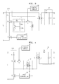
- FIG. 1 is a circuit diagram of a switch mode power supply apparatus according to an embodiment of the present invention.
- the switch mode power supply apparatus according to the current embodiment is shown as having a single output, it is understood that embodiments of the present invention can be implemented to output N supply voltages in which N is a natural number. Further, if the number of outputs is N, a transformer can have N secondary coils, and each secondary coil can be connected to one of or a number of a plurality of secondary output circuits.
- the switch mode power supply apparatus includes a transformer T having a primary coil L 1 and a secondary coil L 2 , which has a predetermined turn ratio with respect to the primary coil L 1 .
- the primary coil L 1 is connected to a primary circuit
- the secondary coil L 2 is connected to an output circuit.
- the primary circuit is insulated from the output circuit by the transformer T.
- the primary circuit includes a main switching device Qi, a Pulse Width Modulation (PWM) controller 30 to control the main switching device Qi by generating a PWM signal as a switching control signal, an active clamping circuit 10 to perform a clamping operation to suppress a voltage stress of the main switching device Qi.
- the active clamping circuit 10 may be a self-driven type active clamping circuit.
- the main switching device Qi performs a switching operation in response to a switching control signal supplied by the PWM controller 30, thereby controlling the transformer T to charge or transfer energy. Meanwhile, the PWM controller 30 can control the switching operation of the main switching device Qi by using an output voltage of the output circuit.
- the output circuit includes a rectifier 20 to rectify a supply voltage transferred to the secondary coil L 2 of the transformer T.
- the rectifier 20 may be a half-wave rectifier circuit including a diode D2 and a capacitor C2.
- the embodiments of the present invention are not limited thereto, and the rectifier 20 can be any type of rectifier circuit.
- output terminals to output output voltages can be formed at both terminals of the capacitor C2.
- the active clamping circuit 10 includes an auxiliary coil L 3 , which is coupled with the primary coil L 1 , a first switching device Qc, and a clamping capacitor Cc, in order to perform a clamping operation.
- the active clamping circuit 10 further includes a second switching device S to enable or disable the clamping operation.
- the first switching device Qc may be a Metal Oxide Semiconductor Field Effect Transistor (MOSFET) as illustrated in FIG. 1 , and a gate terminal of the first switching Qc may include a driving circuit to drive the first switching device Qc.
- MOSFET Metal Oxide Semiconductor Field Effect Transistor
- the auxiliary coil L 3 which is coupled with the primary coil L 1 , generates a first control signal for turning on or off the first switching device Qc, and the first control signal is input to the gate of the first switching device Qc. While an input voltage Vi is applied to the primary coil L 1 by turning on the main switching device Qi, the first switching device Qc is turned off according to the first control signal. If the main switching device Qi is turned off, and the first switching device Qc is turned on according to the first control signal, the active clamping circuit 10 operates to discharge energy accumulated in the transformer T and simultaneously clamp a voltage stress of the main switching device Qc to a sum value of the input voltage Vi and a voltage at both terminals of the clamping capacitor Cc. The clamping operation of the active clamping circuit 10 is performed while the second switching device S is turned on.
- the control circuit 40 turns on the second switching device S when the switch mode power supply apparatus is in a normal operating mode, and turns off the second switching device S when the switch mode power supply apparatus is in a standby mode. Therefore, the control circuit 40 enables the clamping operation of the active clamping circuit 10 in the normal operating mode, and disables the clamping operation of the active clamping circuit 10 in the standby mode.
- the second switching device S can be implemented using a photocoupler, a Bipolar Junction Transistor (BJT), a MOSFET, or the like. If the second switching device S is implemented using a photocoupler, the control circuit 40 may includes a photodiode and the second switching device S may be a phototransistor.
- the standby mode minimizes power consumption, and can be set when a very small load is applied to the output terminals of the output circuit, or when a control signal is received from a control apparatus, such as a micom, which is installed outside the switch mode power supply apparatus.
- FIG. 2 is a circuit diagram of a switch mode power supply apparatus according to another embodiment of the present invention.
- an external-driven type active clamp circuit is used.
- the switch mode power supply apparatus according to FIG. 2 includes a single output, it is understood that the switch mode power supply apparatus according to aspects of the present invention can be implemented to output N supply voltages.
- the clamping operation of an active clamping circuit 11 is performed according to a second control signal from a PWM controller 31.
- the operation of the switch mode power supply apparatus according to the current embodiment is substantially similar to that of the switch mode power supply apparatus illustrated in FIG. 1 .
- the PWM controller 31 generates a first or switching control signal to control the switching operation of a main switching device Qi, and a second control signal to control the switching operation of a first switching device Qc.
- the main switching device Qi is turned on or off in response to the switching control signal supplied from the PWM controller 31, thereby allowing a transformer T to charge or transfer energy. Meanwhile, the PWM controller 31 can control the switching operation of the main switching device Qi using an output voltage of an output circuit.
- the active clamping circuit 11 includes the first switching device Qc and a clamping capacitor Cc to perform a clamping operation, and a second switching device S to enable or disable the clamping operation, as in the switch mode power supply apparatus illustrated in FIG. 1 .
- the first switching device Qc as illustrated in FIG. 2 , may be a MOSFET, and can include a driving circuit (not illustrated in FIG. 2 ) which is connected to the gate of the first switching device Qc and drives the first switching terminal Qc.
- the PWM controller 31 applies the switching control signal and the second control signal to the main switching device Qi and the first switching device Qc, respectively, so that the main switching device Qi and the first switching device Qc are driven in a manner to be complementary to each other.
- the PWM controller 31 applies a second control signal for turning on the first switching device Qc to the first switching device Qc, if the switching control signal indicates tuning off of the main switching device Qi, and applies a second control signal for turning off the first switching device Qc to the first switching device Qc, if the switching control signal indicates turning on of the main switching device Qi. Accordingly, while an input voltage is applied to a primary coil L 1 , due to the turning on of the main switching device Qi, the first switching device is turned off.
- the active clamping circuit 11 operates to discharge energy accumulated in the transformer T and simultaneously clamp a voltage stress of the main switching device Qc to a sum value of an input voltage Vi and a voltage at both terminals of the clamping capacitor Cc.
- the clamping operation of the active clamping circuit 11 is performed while the second switching device S is turned on.
- FIG. 3 is a circuit diagram of a switch mode power supply apparatus in which a dead-time control circuit 13 is added to the active clamping circuit 10A of the switch mode power supply apparatus illustrated in FIG. 1 , according to another embodiment of the present invention.
- the dead-time control circuit 13 is connected to the gate of the first switching device Qc.
- a dead time required to turn on a switching device when the other switching device is completely turned off decreases switching loss and a voltage stress that occur in a period in which a main switching device Qi and a first switching device Qc are simultaneously turned on.
- the dead time control circuit 13 controls such a dead time and includes a bipolar junction transistor (BJT) Td, resistors Rd1 and Rd2, and capacitors Cd1 and Cd2.
- BJT bipolar junction transistor
- Rd1 and Rd2 resistors Rd1 and Rd2
- capacitors Cd1 and Cd2 capacitors
- a collector of the BJT Td is connected to the gate of the first switching device Qc and the resistor Rd1 while the emitter is connected to the primary coil L 1 , of the transistor T.
- a base of the BJT Td is connected between the resistor Rd2 and the capacitor Cd2.
- the resistor Rd2 is further connected between the resistor Rd1 and the capacitor Cd1, which is connected to the second switching device S.
- FIG. 4 is a circuit diagram of a switch mode power supply apparatus in which a pulse transformer is added to an active clamping circuit of the switch mode power supply apparatus illustrated in FIG. 2 , according to another embodiment of the present invention.
- an active clamping circuit 11A of the switch mode power supply apparatus includes a pulse transformer 14 which is connected to an input terminal to receive a control signal from a PWM controller 31.
- the pulse transformer 14 receives a control signal from the PWM controller 31, converts the control signal into a voltage capable of driving a first switching device Qc, and insulates the PWM controller 31 from the first switching device Qc.
- FIG. 5 is a circuit diagram of a switch mode power supply apparatus in which bootstrap circuits 15 and 16 are added to the gate of the main switching device Qi and the active clamping circuit 11 B of the switch mode power supply apparatus illustrated in FIG. 2 , according to another embodiment of the present invention.
- bootstrap circuit 15 By adding the bootstrap circuit 15 to the gate of a first switching device Qc, a switching operation can be more stably performed.
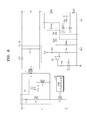
- FIG. 6 is a circuit diagram of a switch mode power supply apparatus including a control circuit 40A according to an embodiment of the present invention.
- the switch mode power supply apparatus according to the current embodiment of the present invention includes an active clamping circuit 10 which is the same as the active clamping circuit 10 illustrated in FIG. 1 .
- aspects of the present invention are not limited thereto, and one of the active clamping circuits 11, 10A, 11A and 11 B included in the switch mode power supply apparatuses illustrated in FIGS. 2 through 5 , respectively, can also be used in the switch mode power supply apparatus of FIG. 6 .
- the control circuit 40A generates a control signal for enabling or disabling the clamping operation of the active clamping circuit 10, according to an output voltage of an output circuit of the switch mode power supply apparatus. As described above, when a very small load is applied to an output terminal of the output circuit, the switch mode power supply apparatus enters a standby mode.
- control circuit 40A disables the operation of the active clamping circuit 10 when the output voltage of the control circuit 40A exceeds a predetermined voltage.
- the control circuit 40A includes a resistor Ra1 having a first terminal connected to an output terminal of the output circuit, a diode Da having an anode connected to a second terminal of the resistor Ra1, a resistor Ra2 having a first terminal connected to the cathode of the diode Da, a resistor Ra3 connected between a second terminal of the resistor Ra2 and a ground, a resistor Ra4 having a first terminal connected to a supply voltage source Vcc, a resistor Ra5 connected between a second terminal of the resistor Ra4 and the ground, a comparator 42 whose negative (-) terminal is connected to the second terminal of the resistor Ra2 and whose positive (+) terminal is connected to a first terminal of the resistor Ra5, a resistor Ra6 having a first terminal connected to an output terminal of the comparator 42, and a photodiode PC1-1 whose anode is connected to a second terminal of the resistor Ra6 and whose cathode is connected to the ground.
- the second switching device S is implemented using a photocoupler comprising the photodiode PC1-1 and the phototransistor PC1-2.
- An output voltage is detected with a predetermined ratio by the resistors Ra1, Ra2, and Ra3, and provided to the negative (-) terminal of the comparator 42.
- the diode Da prevents a current from flowing from the comparator 42 to the output terminal of the output circuit.
- the supply voltage Vcc is divided by the resistors Ra4 and Ra5 so that a predetermined reference voltage is applied to the positive (+) terminal of the comparator 42.
- the photodiode PC1-1 and the resistor Ra6 connected to the output terminal of the comparator 42 so that the photodiode PC1-1 emits light and the phototransistor PC1-2 is turned on.
- the output voltage detected with the predetermined ratio is higher than the predetermined reference voltage
- no current flows to the output terminal of the comparator 42 so that the photodiode PC1-1 emits no light and the phototransistor PC1-2 is turned off. Accordingly, if the output voltage exceeds the predetermined reference voltage, the phototransistor PC1-2 is turned off and thus the clamping operation of the active clamping circuit 10 is disabled.
- the switch mode power supply apparatus includes an output voltage feedback circuit 50 which feeds back information about the output voltage to the PWM controller 30.
- the output voltage feedback circuit 50 includes a resistor Ra1 having a first terminal connected to an output terminal of the output circuit, a photodiode PC2 having an anode connected to a second terminal of the resistor Ra1, a shunt regulator SR having a cathode connected to the cathode of the photodiode PC2 and an anode connected to a ground, a resistor Rf1 connected between an output terminal of the output circuit and a reference terminal of the shunt regulator SR, a resistor Rf3 connected between the reference terminal of the shunt regulator SR and the ground, a resistor Rf2 connected in series between the cathode of the photodiode PC2 and a first terminal of the resistor Rf3, and a capacitor Cf.
- the photodiode PC2 outputs a signal corresponding to information about an output voltage, to
- FIG. 7 is a circuit diagram of a switch mode power supply apparatus including a control circuit 40B, according to another embodiment of the present invention.
- the switch mode power supply apparatus according to the current embodiment of the present invention includes an active clamping circuit 10 which is the same as the active clamping circuit 10 of the switch mode power supply apparatus illustrated in FIG. 1 .
- aspects of the present invention are not limited thereto, and one of the active clamping circuits 11, 10A, 11A and 11 B included in the switch mode power supply apparatuses illustrated in FIGs. 2 through 5 , respectively, can also be used in the switch mode power supply apparatus of FIG. 7 .
- the control circuit 40B generates a control signal to enable or disable the clamping operation of the active clamping circuit 10, according to a current which flows through a primary circuit, that is, according to a current which flows through a main switching device Qi of the switch mode power supply apparatus.
- a current which flows through the primary circuit becomes very small.
- a resistor Rb1 is provided in order to sense a current which flows through the main switching device Qi between the main switching device Qi and a ground.
- the operation of the active clamping circuit 10 is disabled when a voltage across the resistor Rb1 is lower than a predetermined voltage.
- the control circuit 40B includes a resistor Rb1 having a first terminal connected to the main switching device Qi and a second terminal connected to a ground, a resistor Rb2 having a first terminal connected to the first terminal of the resistor Rb1, a resistor Rb3 connected between a second terminal of the resistor Rb2 and the ground, a resistor Rb4 having a first terminal connected to a supply voltage source Vcc, a resistor Rb5 connected between a second terminal of the resistor Rb4 and the ground, a comparator 44 whose negative (-) terminal is connected to the second terminal of the resistor Rb2 and whose positive (+) terminal is connected to a second terminal of the resistor Rb4 and a first terminal of the resistor Rb5, a resistor Rb6 having a first terminal connected to an output terminal of the comparator 42, and a photodiode PC3-1 whose anode is connected to a second terminal of the resistor Rb6 and whose cathode is connected to the
- the second switching device S is implemented using a photocoupler comprising the photodiode PC3-1 and a phototransistor PC3-2.
- a voltage across the resistor Rb1 is detected with a predetermined ratio by the resistors Rb2 and Rb3 and provided to the positive (+) terminal of the comparator 44.
- the supply voltage Vcc is divided by the resistors Rb4 and Rb5 so that a predetermined reference voltage is provided to the negative (-) terminal of the comparator 44. If the voltage across the resistor Rb1, which is detected with a predetermined ratio, is higher than the predetermined reference voltage, a current flows through the photodiode PC3-1 and the resistor Rb6 connected to the output terminal of the comparator 44, so that the photodiode PC3-1 emits light and the phototransistor PC3-2 is turned on.
- the phototransistor PC3-2 is turned off and the clamping operation of the active clamping circuit 10 is disabled.
- FIG. 8 is a circuit diagram of a switch mode power supply apparatus including a control circuit 40C, according to another embodiment of the present invention.
- the switch mode power supply according to the current embodiment of the present invention includes an active clamping circuit 10 which is the same as the active clamping circuit 10 illustrated in FIG. 1 .
- aspects of the present invention are not limited thereto, and one of the active clamping circuits 11, 10A, 11A and 11 B included in the switch mode power supply apparatuses illustrated in the FIGs. 2 through 5 , respectively, can also be used in the switch mode power supply apparatus of FIG. 8 .
- the control circuit 40C generates a control signal to enable or disable the clamping operation of the active clamping circuit 10, according to a control signal which is received from a control apparatus (not shown), such as a micom, which is installed outside the switch mode power supply apparatus.
- a standby mode signal is generated by the control apparatus which is installed outside the switch mode power supply apparatus, and indicates whether the switch mode power supply apparatus is in a standby mode. For example, if the standby mode signal is in a "high” state, it indicates a normal operating mode, and if the standby mode signal is in a "low” state, it indicates a standby mode.
- the control circuit 40C includes a resistor Rc having a first terminal connected to an output terminal of an output circuit of the switch mode power supply apparatus and a second terminal connected to a standby mode signal output terminal of the control apparatus, and a photodiode PC4-1 having an anode connected to the second terminal of the resistor Rc and a cathode connected to a ground.
- a second switching device S is implemented using a photo coupler comprising a photodiode PC4-1 and a phototransistor PC4-2. If a standby mode signal is in a "high" state indicating a normal operating mode, a current flows through the photodiode PC4-1, so that the photodiode PC4-1 emits light and the phototransistor PC4-2 is turned on.
- the standby mode signal is in a "low" state indicating a standby mode
- no current flows through the photodiode PC4-1, so that the photodiode PC4-1 emits no light and thus the phototransistor PC4-2 is turned off.
- a standby mode signal received by the control apparatus which is installed outside the switch mode power supply apparatus indicates a standby mode
- the phototransistor PC4-2 is turned off and thus the clamping operation of the active clamping circuit 10 is disabled.
- the switch mode power supply apparatus when the switch mode power supply apparatus according to aspects of the present invention is in a standby mode, the clamping operation of an active clamping circuit of the switch mode power supply apparatus is not performed. Accordingly, in the standby mode, a circulating path of a current is not formed in the primary circuit when the main switching device is turned off, and thus a power loss of a transformer, etc., which is caused by such current flow, is significantly reduced. Also, since the clamping operation of the active clamping circuit is not performed in the standby mode, the switch mode power supply apparatus can operate in a discontinuous conduction mode (DCM).
- DCM discontinuous conduction mode
- the active clamping circuit by allowing the active clamping circuit to perform a clamping operation in a normal operating mode, it is possible to suppress a voltage stress of a main switching device, reduce switching loss, reuse energy, and thereby improve power conversion efficiency. Also, in a standby mode, by reducing power loss of a transformer, etc., which is caused by a current flowing through the primary circuit, and allowing the switch mode power supply apparatus to operate in a discontinuous conduction mode (DCM), it is possible to significantly reduce power consumption of the switch mode power supply apparatus and thereby improve power consumption efficiency in the standby mode.
- DCM discontinuous conduction mode
Landscapes
- Engineering & Computer Science (AREA)
- Power Engineering (AREA)
- Dc-Dc Converters (AREA)
- Direct Current Feeding And Distribution (AREA)
Applications Claiming Priority (1)
| Application Number | Priority Date | Filing Date | Title |
|---|---|---|---|
| KR20070060683 | 2007-06-20 |
Publications (2)
| Publication Number | Publication Date |
|---|---|
| EP2006985A2 true EP2006985A2 (fr) | 2008-12-24 |
| EP2006985A3 EP2006985A3 (fr) | 2014-09-24 |
Family
ID=39832219
Family Applications (1)
| Application Number | Title | Priority Date | Filing Date |
|---|---|---|---|
| EP08150710.5A Withdrawn EP2006985A3 (fr) | 2007-06-20 | 2008-01-28 | Alimentation à découpage doté d'un circuit de verrouillage actif |
Country Status (4)
| Country | Link |
|---|---|
| US (1) | US8488348B2 (fr) |
| EP (1) | EP2006985A3 (fr) |
| KR (1) | KR101261530B1 (fr) |
| CN (1) | CN101330255A (fr) |
Families Citing this family (28)
| Publication number | Priority date | Publication date | Assignee | Title |
|---|---|---|---|---|
| KR101129391B1 (ko) * | 2007-08-13 | 2012-03-28 | 삼성전자주식회사 | 수동 클램프 회로를 갖는 스위칭 모드 전원공급장치 |
| US20100332857A1 (en) | 2009-06-30 | 2010-12-30 | Vogman Viktor D | Reducing power losses in a redundant power supply system |
| US20110305048A1 (en) * | 2010-06-11 | 2011-12-15 | System General Corp. | Active-clamp circuit for quasi-resonant flyback power converter |
| CN102122890B (zh) * | 2010-10-11 | 2014-01-22 | 南京航空航天大学 | 一种有源钳位反激变换器辅助开关管的控制方法 |
| EP2475087B1 (fr) * | 2011-01-11 | 2016-03-23 | OSRAM GmbH | Dispositif de fourniture d'énergie, par exemple pour sources lumineuses |
| CN102307014A (zh) * | 2011-09-15 | 2012-01-04 | 苏州佳世达电通有限公司 | 根据待机讯号减少待机耗电的电源供应器及电子装置 |
| US8593211B2 (en) * | 2012-03-16 | 2013-11-26 | Texas Instruments Incorporated | System and apparatus for driver circuit for protection of gates of GaN FETs |
| TWI525975B (zh) * | 2013-02-18 | 2016-03-11 | 崇貿科技股份有限公司 | 返馳式功率轉換器之控制電路 |
| US9276483B2 (en) * | 2013-06-27 | 2016-03-01 | System General Corporation | Control circuit for active-clamp flyback power converter with programmable switching period |
| US9077254B2 (en) * | 2013-07-12 | 2015-07-07 | Solantro Semiconductor Corp. | Switching mode power supply using pulse mode active clamping |
| CN103795260B (zh) * | 2014-01-21 | 2016-01-20 | 广州金升阳科技有限公司 | 一种非互补反激有源钳位变换器 |
| US9777864B2 (en) | 2014-09-10 | 2017-10-03 | Continental Automotive Systems, Inc. | Method and device for controlling a solenoid actuator |
| KR101701025B1 (ko) | 2015-02-17 | 2017-02-01 | 삼성전기주식회사 | 전력증폭기용 입력 드라이버 및 송신기 |
| TWM542295U (zh) * | 2015-05-20 | 2017-05-21 | 半導體組件工業公司 | 具有在輕負載下高效操作的切換模式電源供應器 |
| US9991800B2 (en) * | 2015-05-20 | 2018-06-05 | Semiconductor Components Industries, Llc | Switched mode power supply with efficient operation at light loads and method therefor |
| US10193326B2 (en) | 2016-04-21 | 2019-01-29 | Continental Automotive Systems, Inc. | Non-intrusive short-circuit protection for power supply devices |
| US10361638B2 (en) * | 2016-05-04 | 2019-07-23 | Drive Cjsc | Apparatus for generating high pulse voltage |
| WO2017192058A1 (fr) * | 2016-05-04 | 2017-11-09 | Закрытое Акционерное Общество "Драйв" | Procédé pour générer de la haute tension électrique à impulsions dans une charge par induction |
| US9991803B1 (en) * | 2017-01-18 | 2018-06-05 | Semiconductor Components Industries, Llc | Reduction of electromagnetic interference in a flyback converter |
| US10581241B2 (en) * | 2017-06-22 | 2020-03-03 | Silicon Laboratories Inc. | Clamping inductive flyback voltage to reduce power dissipation |
| US10103633B1 (en) * | 2017-08-31 | 2018-10-16 | Dialog Semiconductor (Uk) Limited | Switching converter with power level selection |
| US10418912B2 (en) | 2017-12-21 | 2019-09-17 | Silanna Asia Pte Ltd | Power converter with active clamp |
| US10707766B2 (en) * | 2018-02-02 | 2020-07-07 | Silanna Asia Pte Ltd | Integrated self-driven active clamp |
| TWM561825U (zh) * | 2018-02-12 | 2018-06-11 | Chicony Power Tech Co Ltd | 電源轉換控制電路 |
| US10461626B1 (en) | 2019-01-14 | 2019-10-29 | Silanna Asia Pte Ltd | Active clamp circuit |
| US10673342B1 (en) | 2019-05-02 | 2020-06-02 | Silanna Asia Pte Ltd | Active clamping with bootstrap circuit |
| CN116526849A (zh) * | 2022-01-20 | 2023-08-01 | 捷拓科技股份有限公司 | 自激式主动箝位电路 |
| CN121666692A (zh) * | 2023-08-03 | 2026-03-13 | 斯凯利股份有限公司 | 电力控制的方法和系统 |
Family Cites Families (7)
| Publication number | Priority date | Publication date | Assignee | Title |
|---|---|---|---|---|
| JP3198944B2 (ja) * | 1995-11-17 | 2001-08-13 | 株式会社村田製作所 | スイッチング電源装置 |
| JP2001112254A (ja) * | 1999-10-06 | 2001-04-20 | Toshiba Corp | 電源回路 |
| US6466462B2 (en) | 2000-10-31 | 2002-10-15 | Yokogawa Electric Corporation | DC/DC converter having a control circuit to reduce losses at light loads |
| JP3707409B2 (ja) | 2001-09-10 | 2005-10-19 | 株式会社村田製作所 | スイッチング電源装置 |
| US7006364B2 (en) * | 2004-03-15 | 2006-02-28 | Delta Electronics, Inc. | Driving circuit for DC/DC converter |
| KR100636241B1 (ko) * | 2005-06-16 | 2006-10-19 | 삼성전자주식회사 | 능동적 로드 검출 스위칭 모드 파워 서플라이 및 그 스위칭방법 |
| US7286376B2 (en) * | 2005-11-23 | 2007-10-23 | System General Corp. | Soft-switching power converter having power saving circuit for light load operations |
-
2008
- 2008-01-09 US US11/971,406 patent/US8488348B2/en not_active Expired - Fee Related
- 2008-01-15 KR KR1020080004440A patent/KR101261530B1/ko not_active Expired - Fee Related
- 2008-01-28 EP EP08150710.5A patent/EP2006985A3/fr not_active Withdrawn
- 2008-02-22 CN CNA2008100814714A patent/CN101330255A/zh active Pending
Also Published As
| Publication number | Publication date |
|---|---|
| US8488348B2 (en) | 2013-07-16 |
| EP2006985A3 (fr) | 2014-09-24 |
| KR20080112085A (ko) | 2008-12-24 |
| US20080315858A1 (en) | 2008-12-25 |
| CN101330255A (zh) | 2008-12-24 |
| KR101261530B1 (ko) | 2013-05-07 |
Similar Documents
| Publication | Publication Date | Title |
|---|---|---|
| EP2006985A2 (fr) | Alimentation à découpage doté d'un circuit de verrouillage actif | |
| KR101931448B1 (ko) | 스타트업 셀 회로의 시스템 및 방법 | |
| US7696733B2 (en) | Resonant switching power source device | |
| US10135350B2 (en) | AC/DC converters with wider voltage regulation range | |
| US10637363B2 (en) | Converters with hold-up operation | |
| US9812977B2 (en) | Resonant converters with an improved voltage regulation range | |
| EP2713488B1 (fr) | Convertisseur électronique et système d'éclairage associé et procédé de fonctionnement d'un convertisseur électronique | |
| JP5584089B2 (ja) | 力率を増加させた駆動回路 | |
| US9490708B2 (en) | Multiple-output DC/DC converter and power supply having the same | |
| US8885370B2 (en) | Current-fed isolation converter | |
| US20140133200A1 (en) | Clamp snubber circuit and resistance adjustment method for the same | |
| CN101369779B (zh) | 具有无源箝位电路的切换模式电源装置 | |
| US9356526B2 (en) | DC-DC power conversion apparatus and method | |
| TW201929404A (zh) | 應用在返馳式轉換器的可調式降頻曲線技術 | |
| US9537412B2 (en) | Direct current voltage conversion device and clamping circuit | |
| US20080259649A1 (en) | Switched mode power supply comprising a rectifier circuit | |
| US6980447B1 (en) | Active snubber circuit for synchronous rectifier | |
| US20120044729A1 (en) | Bridgeless coupled inductor boost power factor rectifiers | |
| US12355345B2 (en) | Power supply capable of stabilizing and compensating resonant voltages | |
| US9130472B2 (en) | High efficient single switch single stage power factor correction power supply | |
| US9490717B2 (en) | Switching power supply circuit | |
| US6999325B2 (en) | Current/voltage converter arrangement | |
| KR102142630B1 (ko) | 전압구동형 동기정류기 구동회로 | |
| KR20210106702A (ko) | 고압 인버터 장치의 전원공급회로 | |
| US11837950B2 (en) | Switching power supply and electronic device |
Legal Events
| Date | Code | Title | Description |
|---|---|---|---|
| PUAI | Public reference made under article 153(3) epc to a published international application that has entered the european phase |
Free format text: ORIGINAL CODE: 0009012 |
|
| AK | Designated contracting states |
Kind code of ref document: A2 Designated state(s): AT BE BG CH CY CZ DE DK EE ES FI FR GB GR HR HU IE IS IT LI LT LU LV MC MT NL NO PL PT RO SE SI SK TR |
|
| AX | Request for extension of the european patent |
Extension state: AL BA MK RS |
|
| RAP1 | Party data changed (applicant data changed or rights of an application transferred) |
Owner name: SAMSUNG ELECTRONICS CO., LTD. |
|
| 17P | Request for examination filed |
Effective date: 20130312 |
|
| PUAL | Search report despatched |
Free format text: ORIGINAL CODE: 0009013 |
|
| AK | Designated contracting states |
Kind code of ref document: A3 Designated state(s): AT BE BG CH CY CZ DE DK EE ES FI FR GB GR HR HU IE IS IT LI LT LU LV MC MT NL NO PL PT RO SE SI SK TR |
|
| AX | Request for extension of the european patent |
Extension state: AL BA MK RS |
|
| RIC1 | Information provided on ipc code assigned before grant |
Ipc: H02M 1/00 20070101ALI20140815BHEP Ipc: H02M 1/34 20070101ALI20140815BHEP Ipc: H02M 3/335 20060101AFI20140815BHEP |
|
| AKX | Designation fees paid |
Designated state(s): DE FR GB NL |
|
| AXX | Extension fees paid |
Extension state: MK Extension state: RS Extension state: AL Extension state: BA |
|
| STAA | Information on the status of an ep patent application or granted ep patent |
Free format text: STATUS: THE APPLICATION IS DEEMED TO BE WITHDRAWN |
|
| 18D | Application deemed to be withdrawn |
Effective date: 20150325 |