EP2007009A2 - Planares Emi-Filter - Google Patents
Planares Emi-Filter Download PDFInfo
- Publication number
- EP2007009A2 EP2007009A2 EP08252033A EP08252033A EP2007009A2 EP 2007009 A2 EP2007009 A2 EP 2007009A2 EP 08252033 A EP08252033 A EP 08252033A EP 08252033 A EP08252033 A EP 08252033A EP 2007009 A2 EP2007009 A2 EP 2007009A2
- Authority
- EP
- European Patent Office
- Prior art keywords
- filter
- planar
- emi
- power source
- active
- Prior art date
- Legal status (The legal status is an assumption and is not a legal conclusion. Google has not performed a legal analysis and makes no representation as to the accuracy of the status listed.)
- Withdrawn
Links
- 238000004804 winding Methods 0.000 claims abstract description 44
- 239000003990 capacitor Substances 0.000 claims abstract description 39
- 239000000758 substrate Substances 0.000 claims description 20
- 230000007935 neutral effect Effects 0.000 claims description 15
- 239000003989 dielectric material Substances 0.000 claims description 4
- 230000010354 integration Effects 0.000 abstract description 3
- 238000001914 filtration Methods 0.000 description 13
- 238000003780 insertion Methods 0.000 description 7
- 230000037431 insertion Effects 0.000 description 7
- 230000008878 coupling Effects 0.000 description 6
- 238000010168 coupling process Methods 0.000 description 6
- 238000005859 coupling reaction Methods 0.000 description 6
- 238000012546 transfer Methods 0.000 description 5
- 230000008901 benefit Effects 0.000 description 4
- 238000013461 design Methods 0.000 description 4
- 238000004088 simulation Methods 0.000 description 4
- RYGMFSIKBFXOCR-UHFFFAOYSA-N Copper Chemical compound [Cu] RYGMFSIKBFXOCR-UHFFFAOYSA-N 0.000 description 3
- 229910052802 copper Inorganic materials 0.000 description 3
- 239000010949 copper Substances 0.000 description 3
- 230000001939 inductive effect Effects 0.000 description 3
- 239000000463 material Substances 0.000 description 3
- 238000006842 Henry reaction Methods 0.000 description 2
- 238000010586 diagram Methods 0.000 description 2
- 230000000694 effects Effects 0.000 description 2
- 238000001228 spectrum Methods 0.000 description 2
- 230000001629 suppression Effects 0.000 description 2
- 238000010399 three-hybrid screening Methods 0.000 description 2
- 238000006243 chemical reaction Methods 0.000 description 1
- 238000010276 construction Methods 0.000 description 1
- 238000000151 deposition Methods 0.000 description 1
- 230000004907 flux Effects 0.000 description 1
- 238000005259 measurement Methods 0.000 description 1
- 238000000034 method Methods 0.000 description 1
- 230000004048 modification Effects 0.000 description 1
- 238000012986 modification Methods 0.000 description 1
- 230000003071 parasitic effect Effects 0.000 description 1
- 230000009467 reduction Effects 0.000 description 1
- 239000004065 semiconductor Substances 0.000 description 1
- 230000035899 viability Effects 0.000 description 1
- 229910000859 α-Fe Inorganic materials 0.000 description 1
Images


Classifications
-
- H—ELECTRICITY
- H01—ELECTRIC ELEMENTS
- H01F—MAGNETS; INDUCTANCES; TRANSFORMERS; SELECTION OF MATERIALS FOR THEIR MAGNETIC PROPERTIES
- H01F17/00—Fixed inductances of the signal type
- H01F17/0006—Printed inductances
- H01F17/0013—Printed inductances with stacked layers
-
- H—ELECTRICITY
- H03—ELECTRONIC CIRCUITRY
- H03H—IMPEDANCE NETWORKS, e.g. RESONANT CIRCUITS; RESONATORS
- H03H7/00—Multiple-port networks comprising only passive electrical elements as network components
- H03H7/42—Networks for transforming balanced signals into unbalanced signals and vice versa, e.g. baluns
- H03H7/425—Balance-balance networks
- H03H7/427—Common-mode filters
-
- H—ELECTRICITY
- H01—ELECTRIC ELEMENTS
- H01F—MAGNETS; INDUCTANCES; TRANSFORMERS; SELECTION OF MATERIALS FOR THEIR MAGNETIC PROPERTIES
- H01F17/00—Fixed inductances of the signal type
- H01F17/0006—Printed inductances
- H01F17/0013—Printed inductances with stacked layers
- H01F2017/0026—Multilayer LC-filter
-
- H—ELECTRICITY
- H01—ELECTRIC ELEMENTS
- H01F—MAGNETS; INDUCTANCES; TRANSFORMERS; SELECTION OF MATERIALS FOR THEIR MAGNETIC PROPERTIES
- H01F17/00—Fixed inductances of the signal type
- H01F17/0006—Printed inductances
- H01F2017/0073—Printed inductances with a special conductive pattern, e.g. flat spiral
-
- H—ELECTRICITY
- H03—ELECTRONIC CIRCUITRY
- H03H—IMPEDANCE NETWORKS, e.g. RESONANT CIRCUITS; RESONATORS
- H03H1/00—Constructional details of impedance networks whose electrical mode of operation is not specified or applicable to more than one type of network
- H03H2001/0021—Constructional details
- H03H2001/0078—Constructional details comprising spiral inductor on a substrate
-
- H—ELECTRICITY
- H03—ELECTRONIC CIRCUITRY
- H03H—IMPEDANCE NETWORKS, e.g. RESONANT CIRCUITS; RESONATORS
- H03H1/00—Constructional details of impedance networks whose electrical mode of operation is not specified or applicable to more than one type of network
- H03H2001/0021—Constructional details
- H03H2001/0085—Multilayer, e.g. LTCC, HTCC, green sheets
Definitions
- This invention relates to a planar EMI filter, and in particular to such a filter suitable for use with ultra-high frequency power converters.
- EMI filters are routinely provided with electrical and electronic devices to ensure that any electromagnetic noise generated by the device is not allowed to pass back into the mains power supply.
- filters are classed as being either differential mode (DM) filters comprising inductive elements in the live and neutral lines, or common mode (CM) filters comprising capacitive elements between the live and neutral lines and ground.
- DM differential mode
- CM common mode
- EMI filters are constructed by conventional circuit components including in particular discrete capacitive and inductive components provided on a circuit board.
- EMI filters may become disproportionately large with respect to the associated circuits and components that are being filtered.
- CMSW coreless planar spiral windings
- a CPSW may be formed in a number of ways, for example by depositing conductive tracks on a printed circuit board and when used in a coreless transformer for signal and/or power transfer primary and secondary windings may be formed as CPSWs on opposing sides of a suitable dielectric substrate.
- planar spiral windings have also been proposed for use in integrated EMI filters with the help of ferrite materials. Coupled coreless planar spiral windings have also been proposed to cancel the capacitor parasitic inductance in traditional EMI filters. It has also been known to use CPSW as the inductive elements in differential mode EMI filters, but such prior proposals have always continued to use discrete three-dimensional capacitors that prevent complete integration of the EMI filter structure.
- an EMI filter for use between a power source and an electronic product, wherein the EMI filter comprises at least one planar element comprising a pair of opposed coreless spiral planar windings, and a planar capacitor.
- planar windings are formed on opposed sides of a substrate, such as for example a printed circuit board.
- the planar capacitor may comprise at least two parallel conductive plates spaced apart by a dielectric material.
- the filter is preferably a combined conductive mode filter and differential mode filter.
- the conductive mode filter may comprise a first planar element
- the differential mode filter may comprises two planar elements symmetrically disposed in the phase and neutral lines between the power source and the product.
- the common mode filter is provided adjacent the power source and the differential mode filter is provided adjacent the product.
- the planar capacitor may be provided between the common mode filter and the differential mode filter, or between the differential mode filter and the product, or between the power source and the common mode filter.
- the differential mode filter may be provided adjacent to the power source and the common mode filter may be provided adjacent to the product.
- the planar capacitor may be provided between the power source and the differential mode filter, or between the differential mode filter and the common mode filter, or between the common mode filter and the product.
- planar windings are formed such that alternate rings of each of the spiral winding are formed on opposite sides of a substrate and are electrically interconnected by vias whereby each side of the substrate is formed with alternating rings belonging to the respective spiral windings.
- planar EMI filter of embodiments of the invention may be combined with an active filter element that may be provided at the middle-stage, at the end-stage or at both the middle- and end-stage of the filter.
- an EMI filter comprising a passive filter and an active filter wherein said passive filter comprises at least one planar element comprising a pair of opposed coreless spiral planar windings, and a planar capacitor.
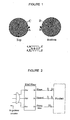
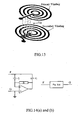
- FIG. shows two conventional spiral windings.
- the dimensions and number of turns of the windings may vary depending on the intended application.
- the windings can be constructed with printed circuit board (PCB) or other substrates such as semiconductor materials.
- PCB printed circuit board
- the windings may be formed on opposed sides of a PCB substrate, eg 0.4mm thick and may form the primary and secondary coils of a coreless transformer as is known in the art.
- the ends of the top coil may be labeled A and C, while the corresponding ends of the bottom coil may be labeled B and D.
- the two planar spiral windings when placed on opposite sides of a substrate the two planar spiral windings may be represented electrically as two inductances with a capacitive component between them.
- FIG.2 shows a simple block diagram of the function of an EMI filter.
- the function of the EMI filter is to block and/or divert the conducted emission current in common mode (I C ) and differential mode (I D ) so that they do not enter the power source.
- FIG.3a shows how two planar spiral windings formed on opposed sides of a substrate may be employed as a DM filter added on the phase line.
- the phase line from the power source is connected at A and the phase line from the filter to the device goes from C.
- Point B is connected to earth.
- FIG.3b shows how the same windings can be employed as a DM filter added on the neutral line.
- point A is connected alone to the phase line, while the neutral line from the power source is connected at point B and the neutral line goes from point D to the device.
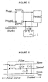
- planar CM and DM filter elements may employ one or more planar capacitors an example of which is shown in FIG.4 .
- this planar capacitor may comprise three planar copper layers in a sandwich-like structure and separated by dielectric layers.
- the three copper layers may respectively be connected to the phase, earth and neutral lines as may be required in any particular circuit diagrams.
- typical dimensions may be 40mm x 40mm x 0.07mm for the copper layers, and a thickness of 0.36mm for the interleaving dielectric layers.
- the dielectric material may be a simple PCB substrate, or may be a material of higher permittivity if a higher capacitance is required.
- FIG.5 shows how a planar capacitor 1 may be used in conjunction with a planar spiral winding structure to form a common mode filter.
- the planar spiral windings are connected in the phase and neutral lines between the power source and the product with the phase line from the power source being connected at A and the phase line extending to the product from C. Similarly the neutral line from the power source is connected at B and the neutral line continues to the product from D.
- a planar capacitor 1 constructed as shown in Fig.4 is connected between the spiral windings and the product, with the neutral, phase and earth layers of the capacitor 1 being connected to the respective neutral, phase and earth lines.
- FIG.6 shows how this is done in a conventional EMI filter.
- a conventional combined filter normally consists of a CM choke as well as CM capacitors and a DM capacitor as shown in FIG.6 .
- Such a conventional design can be looked at as a CM filter with a DM capacitor added, but when a CM choke is used in a DM filter only a very small leakage inductance remains effective for filtering because of flux cancellation and so a large capacitor C D is needed to achieve the required filtering effect.
- Providing such a large capacitance in a planar capacitor structure as shown in FIG.4 requires either an undesirably large area, or a dielectric material of high permittivity.
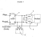
- FIG.7 shows a combined CM and DM filter using planar spiral windings and planar capacitors that mitigates this problem.
- two DM filters 2,3 respectively of the forms shown in FIG.3a and FIG.3b and with filter 2 added to the phase line and filter 3 added to the neutral line.
- These two DM filters provide the DM EMI filtering while retaining filter circuit symmetry.
- CM filtering is provided by CM filter 4 which is of the form shown in FIG.5 including the planar capacitor 5. It will be noted that terminal C in the CM filter - which is in the phase line - connects to terminals A in both the DM filters, while terminal D in the CM filter - which is in the neutral line - connects to terminals B in the DM filters.
- One advantage of this circuit design is that the capacitive elements in the CM filter - both the planar capacitor and the distributed capacitance in the spiral windings - contributes to the overall DM filtering.
- the combined filter of FIG.7 may be considered to have the structure CM choke + C + DM filter.
- FIG.8 shows a modification of the embodiment of FIG.7 in which instead of being provided between the CM and DM spiral windings, the planar capacitor 5 is instead provided between the DM filters the electrical product.
- This structure is therefore CM choke + DM filter + C.
- a further possibility is the sequence C + CM choke + DM filter as shown in FIG.9 where the planar capacitor is located between the power source and the CM choke.
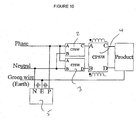
- FIG.10 has the structure C + DM filter + CM choke with the planar capacitor being located between the power source and the DM filter.
- the planar capacitor is located between the DM filter and the CM choke, ie DM filter + C + CM choke, while finally in FIG.12 the planar capacitor is located between the CM choke and the product, ie the structure is DM filter + CM choke + C.
- a stacked spiral winding structure can be used for the planar windings in which the winding structure comprises turns alternately on both sides of the substrate as shown in FIG.13 .
- a first winding starts from the centre of the spiral, and after the first loop the winding passes through the substrate by means of a via such that the second loop is on the opposite side of the substrate from the first. After the second loop the winding returns by means of another via to the first side of the substrate and the winding thus alternates between the two sides of the substrate.
- the second winding starts on the opposite side of the substrate from the first winding and like the first winding alternates from side of the substrate to the other.
- planar EMI filter of embodiments of the present invention may also advantageously be used in combination with an active filter to provide effective noise suppression over a very wide bandwidth.
- active EMI filters Four basic types of active EMI filters have been proposed ( Thomas Farkas and Martin F. Schlecht, "Viability of Active EMI Filters for Utility Applications", IEEE Transactions on Power Electronics, Vol.9, No.3, May 1994, pp.328-336 ; David C. Hamili, "An Efficient Active Ripple Filter for Use in DC-DC Conversion", IEEE Transactions on Aerospace and Electronic Systems, Vol.32, No.3, July 1996, pp.1077-1084 ; N.K.Poon, J.C.P. Liu, C.K. Tse, and M.H.
- an active filter in the form of a voltage feed-forward sensing and active coupling active filter will be used.
- the active filter consists of an operational amplifier and two shunt capacitors C f and C o connected at both the input and output of the operational amplifier as shown in FIG.14(a) .
- the active filter is treated as a building block with terminals F and G as shown in FIG.14(b) where port G is always connected to ground.
- FIG. 15 is a schematic view illustrating how a hybrid passive and active integrated EMI filter may be constructed.
- the blocks labeled "P” comprises planar EMI filters in accordance with embodiments of the invention, while blocks labeled "Q" comprise active filter blocks as shown in FIG.14(b) .
- FIG.15 shows several possible locations for the active components which may be located at the middle-stage, the end-stage or both the middle- and end-stages of the planar EMI filter.
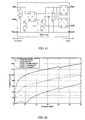
- EMI Filter Description Building Blocks EMI Filter I (passive filter) Coreless planar spiral winding (CPSW) based EMI filter P1 + P2 + P3 EMI Filter II (active filter) Single-stage active filter Q3 + Q4 EMI Filter III (hybrid filter-1) CPSW based + middle-stage active filter P1 + P2 + P3 + Q1 + Q2 EMI Filter IV (hybrid filter-2) CPSW based + end-stage active filter P1 + P2 + P3 + Q3 + Q4 EMI Filter V (hybrid filter-3) CPSW based + two-stage active filter P1 + P2 + P3 + Q1 + Q2 + Q3 + Q4
- FIG. 16 shows the simulated results of common-mode insertion-loss performances of the EMI filter I to EMI filter V (as defined in the table above). These results indicate that a simple passive CPSW based filter (Filter I) can have high insertion loss ability beyond 10MHz.
- the 1-stage active filter (Filter II) has a high insertion loss at the relatively low frequency range (from kHz to 10 MHz) but lower insertion loss than Filter I beyond 10MHz.
- the presence of active blocks can boost up insertion loss of the CPSW based filter at low end frequency region (below MHz) significantly so that Filters III to V can achieve good insertion losses over a wide bandwidth for EMI reduction.
- the different filter configurations considered in the above Table can also be put into an EMI simulation model emulating a 20W converter running at 1MHz with differential-mode noise generated by an input current source flowing through the input bulk capacitor's equivalent series resistance (ESR).
- ESR equivalent series resistance
- the common-mode noise generation is more complicated and is based on the concept of non-contact coupling paths due to capacitive and inductance coupling.
- the use of non-contact coupling for common-mode noise would make the model be more realistic.
- FIG.18 shows the complete simulation schematic with different filter types (Filter I to Filter V) having been simulated one by one.
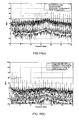
- FIGS.19(a), 19(b) and 19(c) show the simulated results in which FIG.19(a) shows simulated noise for "no filter” (uppermost plot in the figure), “Filter I” (middle plot) and “Filter III” (lowest plot in the figure) (150kHz-30MHz), FIG.19(b) shows simulated EMI noise for "Filter IT' (uppermost plot), “Filter IV' (middle plot) and “Filter V” (lowest plot) (150kHz-30MHz), and FIG.19(c) shows simulated EMI noise for "no filter” (upper plot) and “Filter V” (lower plot) (150kHz-30MHz).
- Filter I CPSW based filter
- the noise level has exceeded the CISPR Class B Limit at the low end of the spectrum.
- Filter III CPSW passive + middle-stage active
- Filter IV CPSW passive + end-stage active
- Filter V (CPSW passive + 2-stage active) has the best filtering performance, reducing the noise level by 20 to 60 dB ⁇ V and passing the CISPR Class B limit line in the entire frequency range. It should be noted that the addition of one more stage of active filter at the input can effectively suppress the common-mode noise coming out from the converter due to both contact or non-contact coupling paths.
- the CPSW based passive filter alone may not pass the CISPR 22 Class B limit line in a 20W converter simulation, but with the addition of 1-stage active filter (end-stage or middle-stage), the filtering performance can reduce noise level by several tens of dBf ⁇ V while adding 2-stage active filtering onto the CPSW based filter can achieve the best performance and the overall system can pass the EMC limit line.
- the proposed hybrid EMI filter offers an effective filtering function over a very wide (30MHz) bandwidth. Such hybrid filter will provide an effective EMI filtering solution to future power converters switching above MegaHertz level.
Landscapes
- Engineering & Computer Science (AREA)
- Power Engineering (AREA)
- Microelectronics & Electronic Packaging (AREA)
- Filters And Equalizers (AREA)
- Coils Or Transformers For Communication (AREA)
Applications Claiming Priority (1)
| Application Number | Priority Date | Filing Date | Title |
|---|---|---|---|
| US11/763,638 US20080309431A1 (en) | 2007-06-15 | 2007-06-15 | Planar emi filter |
Publications (2)
| Publication Number | Publication Date |
|---|---|
| EP2007009A2 true EP2007009A2 (de) | 2008-12-24 |
| EP2007009A3 EP2007009A3 (de) | 2009-12-02 |
Family
ID=39810138
Family Applications (1)
| Application Number | Title | Priority Date | Filing Date |
|---|---|---|---|
| EP08252033A Withdrawn EP2007009A3 (de) | 2007-06-15 | 2008-06-12 | Planares Emi-Filter |
Country Status (3)
| Country | Link |
|---|---|
| US (1) | US20080309431A1 (de) |
| EP (1) | EP2007009A3 (de) |
| CN (1) | CN101409137B (de) |
Cited By (2)
| Publication number | Priority date | Publication date | Assignee | Title |
|---|---|---|---|---|
| US10271422B2 (en) | 2016-05-30 | 2019-04-23 | Hitachi, Ltd. | Printed circuit board for reducing common mode current and a method thereof |
| EP4203221A1 (de) * | 2021-12-22 | 2023-06-28 | Schaffner EMV AG | Filter gegen elektromagnetische interferenz |
Families Citing this family (10)
| Publication number | Priority date | Publication date | Assignee | Title |
|---|---|---|---|---|
| CN101854152B (zh) * | 2010-04-30 | 2012-11-21 | 南京航空航天大学 | 一种圆形pcb线匝构成的平面emi滤波器集成模块 |
| CN101860337B (zh) * | 2010-06-17 | 2012-11-21 | 南京航空航天大学 | 一种基于磁集成的emi滤波器模块 |
| CN103811832B (zh) | 2012-11-08 | 2016-03-09 | 华为技术有限公司 | 滤波器、接收器、发送器和收发器 |
| CN103208914B (zh) * | 2013-03-18 | 2014-12-10 | 南京航空航天大学 | 一种用于大功率场合的平面emi滤波器 |
| US10340788B2 (en) | 2014-12-18 | 2019-07-02 | Telefonaktiebolaget Lm Ericsson (Publ) | Power source interface module with compact EMI filter |
| CN107147280A (zh) * | 2017-06-21 | 2017-09-08 | 山东超越数控电子有限公司 | 一种改善dc‑dc开关电源emi的载板设计方法 |
| CN108051671B (zh) * | 2017-12-08 | 2022-12-13 | 中国核动力研究设计院 | 一种宽频率范围抑制电源线传导发射的装置及方法 |
| CN108595804B (zh) * | 2018-04-13 | 2022-03-04 | 西安理工大学 | 一种高速铁路动车组整车差模emi模型的建立方法 |
| CN108694284B (zh) * | 2018-05-15 | 2022-05-27 | 深圳大学 | 滤波器的参数的计算方法、系统、设备及存储介质 |
| CN114448374B (zh) | 2020-11-04 | 2025-02-18 | 珠海市海米软件技术有限公司 | 一种滤波电路 |
Citations (4)
| Publication number | Priority date | Publication date | Assignee | Title |
|---|---|---|---|---|
| US5583474A (en) | 1990-05-31 | 1996-12-10 | Kabushiki Kaisha Toshiba | Planar magnetic element |
| EP0935263A2 (de) | 1998-02-05 | 1999-08-11 | City University of Hong Kong | Betriebstechniken für kernlose PCB-Transformatoren |
| US20020109573A1 (en) | 1999-05-11 | 2002-08-15 | Nec Corporation | Multilayer printed board with a double plane spiral interconnection structure |
| US20030020583A1 (en) | 2001-06-15 | 2003-01-30 | Hui Ron Shu Yuen | Planar printed-circuit-board transformers with effective electromagnetic interference (emi) shielding |
Family Cites Families (5)
| Publication number | Priority date | Publication date | Assignee | Title |
|---|---|---|---|---|
| US1647474A (en) * | 1923-10-25 | 1927-11-01 | Frederick W Seymour | Variable pathway |
| JPS58220513A (ja) * | 1982-06-16 | 1983-12-22 | Murata Mfg Co Ltd | 電子部品 |
| US5039964A (en) * | 1989-02-16 | 1991-08-13 | Takeshi Ikeda | Inductance and capacitance noise filter |
| JP3027081B2 (ja) * | 1993-12-09 | 2000-03-27 | アルプス電気株式会社 | 薄膜素子 |
| KR100863889B1 (ko) * | 2004-11-25 | 2008-10-15 | 가부시키가이샤 무라타 세이사쿠쇼 | 코일부품 |
-
2007
- 2007-06-15 US US11/763,638 patent/US20080309431A1/en not_active Abandoned
-
2008
- 2008-06-12 EP EP08252033A patent/EP2007009A3/de not_active Withdrawn
- 2008-06-13 CN CN200810144646.1A patent/CN101409137B/zh not_active Expired - Fee Related
Patent Citations (4)
| Publication number | Priority date | Publication date | Assignee | Title |
|---|---|---|---|---|
| US5583474A (en) | 1990-05-31 | 1996-12-10 | Kabushiki Kaisha Toshiba | Planar magnetic element |
| EP0935263A2 (de) | 1998-02-05 | 1999-08-11 | City University of Hong Kong | Betriebstechniken für kernlose PCB-Transformatoren |
| US20020109573A1 (en) | 1999-05-11 | 2002-08-15 | Nec Corporation | Multilayer printed board with a double plane spiral interconnection structure |
| US20030020583A1 (en) | 2001-06-15 | 2003-01-30 | Hui Ron Shu Yuen | Planar printed-circuit-board transformers with effective electromagnetic interference (emi) shielding |
Non-Patent Citations (1)
| Title |
|---|
| HELDWEIN M L ET AL: "Implementation of a Transformer-Less Common Mode Active Filter for Off-Line Converter Systems", APPLIED POWER ELECTRONICS CONFERENCE AND EXPOSITION, 2006. APEC '06. T WENTY-FIRST ANNUAL IEEE MARCH 19, 2006, PISCATAWAY, NJ, USA,IEEE, PISCATAWAY, NJ, USA, 19 March 2006 (2006-03-19), pages 1230 - 1236, XP010910102, ISBN: 978-0-7803-9547-3, DOI: 10.1109/APEC.2006.1620696 * |
Cited By (3)
| Publication number | Priority date | Publication date | Assignee | Title |
|---|---|---|---|---|
| US10271422B2 (en) | 2016-05-30 | 2019-04-23 | Hitachi, Ltd. | Printed circuit board for reducing common mode current and a method thereof |
| EP4203221A1 (de) * | 2021-12-22 | 2023-06-28 | Schaffner EMV AG | Filter gegen elektromagnetische interferenz |
| WO2023119036A1 (en) * | 2021-12-22 | 2023-06-29 | Schaffner Emv Ag | Electromagnetic interference filter |
Also Published As
| Publication number | Publication date |
|---|---|
| US20080309431A1 (en) | 2008-12-18 |
| CN101409137A (zh) | 2009-04-15 |
| CN101409137B (zh) | 2012-05-16 |
| EP2007009A3 (de) | 2009-12-02 |
Similar Documents
| Publication | Publication Date | Title |
|---|---|---|
| EP2007009A2 (de) | Planares Emi-Filter | |
| US8120445B2 (en) | Planar EMI filter comprising coreless spiral planar windings | |
| CN101617570B (zh) | 印刷电路板 | |
| CN111446902B (zh) | 一种用于电机驱动系统的交直流耦合集成式emi滤波器 | |
| US6396362B1 (en) | Compact multilayer BALUN for RF integrated circuits | |
| CN101854152B (zh) | 一种圆形pcb线匝构成的平面emi滤波器集成模块 | |
| Chen et al. | Planar electromagnetic integration technologies for integrated EMI filters | |
| Neugebauer et al. | Filters and components with inductance cancellation | |
| US20110080244A1 (en) | Inductor topologies with substantial common-mode and differential-mode inductance | |
| US6903628B2 (en) | Lowpass filter formed in multi-layer ceramic | |
| CN102594284B (zh) | 一种多线圈集成lc单元构成的平面emi滤波器 | |
| CN104270111A (zh) | 一种共模电感增强结构的母线型emi滤波器 | |
| US12249908B2 (en) | Electrical component and method for manufacturing an electronic component | |
| Huang et al. | A novel integrated multi-elements resonant converter | |
| KR20140076958A (ko) | 하나의 권선으로 구현되는 직렬 인덕터 어레이 및 이를 포함하는 필터 | |
| JP2013115053A (ja) | ノイズ対策電子部品の回路基板への実装構造 | |
| EP4533634A1 (de) | Integrierte induktivität | |
| Ali et al. | Integrated hybrid EMI filter: Study and realization of the active part | |
| WO2023153283A1 (ja) | フィルタ装置、高周波モジュール、および通信装置 | |
| CN104022749B (zh) | 叠层片式emi滤波器 | |
| CN202996476U (zh) | 一种基于重叠交错绕组的平面emi滤波器 | |
| JP6531880B2 (ja) | ノイズ除去回路およびノイズ除去素子 | |
| Ho et al. | A hybrid EMI filter with ultra-wide bandwidth | |
| Neugebauer et al. | Filters and components with inductance cancellation | |
| CN204244072U (zh) | 多通道型dc-dc转换器 |
Legal Events
| Date | Code | Title | Description |
|---|---|---|---|
| PUAI | Public reference made under article 153(3) epc to a published international application that has entered the european phase |
Free format text: ORIGINAL CODE: 0009012 |
|
| AK | Designated contracting states |
Kind code of ref document: A2 Designated state(s): AT BE BG CH CY CZ DE DK EE ES FI FR GB GR HR HU IE IS IT LI LT LU LV MC MT NL NO PL PT RO SE SI SK TR |
|
| AX | Request for extension of the european patent |
Extension state: AL BA MK RS |
|
| PUAL | Search report despatched |
Free format text: ORIGINAL CODE: 0009013 |
|
| AK | Designated contracting states |
Kind code of ref document: A3 Designated state(s): AT BE BG CH CY CZ DE DK EE ES FI FR GB GR HR HU IE IS IT LI LT LU LV MC MT NL NO PL PT RO SE SI SK TR |
|
| AX | Request for extension of the european patent |
Extension state: AL BA MK RS |
|
| 17P | Request for examination filed |
Effective date: 20100519 |
|
| 17Q | First examination report despatched |
Effective date: 20100614 |
|
| AKX | Designation fees paid |
Designated state(s): AT BE BG CH CY CZ DE DK EE ES FI FR GB GR HR HU IE IS IT LI LT LU LV MC MT NL NO PL PT RO SE SI SK TR |
|
| STAA | Information on the status of an ep patent application or granted ep patent |
Free format text: STATUS: THE APPLICATION HAS BEEN WITHDRAWN |
|
| 18W | Application withdrawn |
Effective date: 20130212 |