EP2008769B1 - Poliervorrichtung und Polierverfahren - Google Patents
Poliervorrichtung und Polierverfahren Download PDFInfo
- Publication number
- EP2008769B1 EP2008769B1 EP08011343A EP08011343A EP2008769B1 EP 2008769 B1 EP2008769 B1 EP 2008769B1 EP 08011343 A EP08011343 A EP 08011343A EP 08011343 A EP08011343 A EP 08011343A EP 2008769 B1 EP2008769 B1 EP 2008769B1
- Authority
- EP
- European Patent Office
- Prior art keywords
- polishing
- tape
- substrate
- polishing head
- head
- Prior art date
- Legal status (The legal status is an assumption and is not a legal conclusion. Google has not performed a legal analysis and makes no representation as to the accuracy of the status listed.)
- Active
Links
Images





Classifications
-
- B—PERFORMING OPERATIONS; TRANSPORTING
- B24—GRINDING; POLISHING
- B24B—MACHINES, DEVICES, OR PROCESSES FOR GRINDING OR POLISHING; DRESSING OR CONDITIONING OF ABRADING SURFACES; FEEDING OF GRINDING, POLISHING, OR LAPPING AGENTS
- B24B21/00—Machines or devices using grinding or polishing belts; Accessories therefor
- B24B21/002—Machines or devices using grinding or polishing belts; Accessories therefor for grinding edges or bevels
-
- B—PERFORMING OPERATIONS; TRANSPORTING
- B24—GRINDING; POLISHING
- B24B—MACHINES, DEVICES, OR PROCESSES FOR GRINDING OR POLISHING; DRESSING OR CONDITIONING OF ABRADING SURFACES; FEEDING OF GRINDING, POLISHING, OR LAPPING AGENTS
- B24B9/00—Machines or devices designed for grinding edges or bevels on work or for removing burrs; Accessories therefor
- B24B9/02—Machines or devices designed for grinding edges or bevels on work or for removing burrs; Accessories therefor characterised by a special design with respect to properties of materials specific to articles to be ground
- B24B9/06—Machines or devices designed for grinding edges or bevels on work or for removing burrs; Accessories therefor characterised by a special design with respect to properties of materials specific to articles to be ground of non-metallic inorganic material, e.g. stone, ceramics, porcelain
-
- B—PERFORMING OPERATIONS; TRANSPORTING
- B24—GRINDING; POLISHING
- B24B—MACHINES, DEVICES, OR PROCESSES FOR GRINDING OR POLISHING; DRESSING OR CONDITIONING OF ABRADING SURFACES; FEEDING OF GRINDING, POLISHING, OR LAPPING AGENTS
- B24B21/00—Machines or devices using grinding or polishing belts; Accessories therefor
- B24B21/16—Machines or devices using grinding or polishing belts; Accessories therefor for grinding other surfaces of particular shape
-
- B—PERFORMING OPERATIONS; TRANSPORTING
- B24—GRINDING; POLISHING
- B24B—MACHINES, DEVICES, OR PROCESSES FOR GRINDING OR POLISHING; DRESSING OR CONDITIONING OF ABRADING SURFACES; FEEDING OF GRINDING, POLISHING, OR LAPPING AGENTS
- B24B9/00—Machines or devices designed for grinding edges or bevels on work or for removing burrs; Accessories therefor
- B24B9/02—Machines or devices designed for grinding edges or bevels on work or for removing burrs; Accessories therefor characterised by a special design with respect to properties of materials specific to articles to be ground
- B24B9/06—Machines or devices designed for grinding edges or bevels on work or for removing burrs; Accessories therefor characterised by a special design with respect to properties of materials specific to articles to be ground of non-metallic inorganic material, e.g. stone, ceramics, porcelain
- B24B9/065—Machines or devices designed for grinding edges or bevels on work or for removing burrs; Accessories therefor characterised by a special design with respect to properties of materials specific to articles to be ground of non-metallic inorganic material, e.g. stone, ceramics, porcelain of thin, brittle parts, e.g. semiconductors, wafers
-
- H—ELECTRICITY
- H10—SEMICONDUCTOR DEVICES; ELECTRIC SOLID-STATE DEVICES NOT OTHERWISE PROVIDED FOR
- H10P—GENERIC PROCESSES OR APPARATUS FOR THE MANUFACTURE OR TREATMENT OF DEVICES COVERED BY CLASS H10
- H10P72/00—Handling or holding of wafers, substrates or devices during manufacture or treatment thereof
- H10P72/70—Handling or holding of wafers, substrates or devices during manufacture or treatment thereof for supporting or gripping
- H10P72/76—Handling or holding of wafers, substrates or devices during manufacture or treatment thereof for supporting or gripping using mechanical means, e.g. clamps or pinches
- H10P72/7602—Handling or holding of wafers, substrates or devices during manufacture or treatment thereof for supporting or gripping using mechanical means, e.g. clamps or pinches the wafers being placed on a robot blade or gripped by a gripper for conveyance
-
- H—ELECTRICITY
- H10—SEMICONDUCTOR DEVICES; ELECTRIC SOLID-STATE DEVICES NOT OTHERWISE PROVIDED FOR
- H10P—GENERIC PROCESSES OR APPARATUS FOR THE MANUFACTURE OR TREATMENT OF DEVICES COVERED BY CLASS H10
- H10P72/00—Handling or holding of wafers, substrates or devices during manufacture or treatment thereof
- H10P72/70—Handling or holding of wafers, substrates or devices during manufacture or treatment thereof for supporting or gripping
- H10P72/76—Handling or holding of wafers, substrates or devices during manufacture or treatment thereof for supporting or gripping using mechanical means, e.g. clamps or pinches
- H10P72/7604—Handling or holding of wafers, substrates or devices during manufacture or treatment thereof for supporting or gripping using mechanical means, e.g. clamps or pinches the wafers being placed on a susceptor, stage or support
- H10P72/7626—Handling or holding of wafers, substrates or devices during manufacture or treatment thereof for supporting or gripping using mechanical means, e.g. clamps or pinches the wafers being placed on a susceptor, stage or support characterised by the construction of the shaft
Definitions
- the polishing tape 141 After contacting the periphery of the wafer W, the polishing tape 141 is rewound by the rewind reel 145b.
- the supply reel 145a and the rewind reel 145b are coupled to non-illustrated motors that provide the polishing tape 141 with a suitable tension.
- the polishing head 142 performs a linearly-reciprocating motion in vertical directions, as indicated by arrows in FIG 1 , to thereby provide relative movement between the polishing tape 141 and the wafer W, thus polishing the periphery of the wafer W
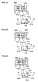
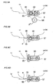
- FIG 4A shows a state in which a center Ch of the polishing head 142 is aligned with a thickness center Cw of the wafer W (which will be hereinafter referred to as simply a wafer center).
- the wafer center Cw is fixed in position during polishing.
- the polishing head 142 performs the linearly-reciprocating motion across the wafer center Cw.
- the pivot of the swinging motion is positioned in the polishing head.
- the polishing tape 41 may comprise a base film having a polishing surface to which abrasive particles, such as diamond particles or SiC particles, are attached.
- the abrasive particles to be attached to the polishing tape 41 are selected in accordance with a type of wafer and a polishing performance required.
- the abrasive particles may be diamond particles or SiC particles having an average diameter in a range of 0.1 ⁇ m to 5.0 ⁇ m.
- the polishing tape 42 may be a belt-shaped polishing cloth with no abrasive particles.
- the base film may comprise a film made from a flexible material, such as polyester, polyurethane, or polyethylene terephthalate.
Landscapes
- Engineering & Computer Science (AREA)
- Mechanical Engineering (AREA)
- Chemical & Material Sciences (AREA)
- Ceramic Engineering (AREA)
- Inorganic Chemistry (AREA)
- Finish Polishing, Edge Sharpening, And Grinding By Specific Grinding Devices (AREA)
- Mechanical Treatment Of Semiconductor (AREA)
- Grinding And Polishing Of Tertiary Curved Surfaces And Surfaces With Complex Shapes (AREA)
Claims (13)
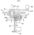
- Ein Poliervorrichtung zum Polieren einer Peripherie eines Substrats durch Vorsehen einer Relativbewegung zwischen einem Polierband (41) und dem Substrat, wobei die Vorrichtung Folgendes aufweist:einen zum Halten des Substrats konfigurierten Halteabschnitt (20);einen Polierkopf (42), konfiguriert um das Polierband (41) in Kontakt mit dem Umfang des Substrats zu bringen;eine Versorgungsspule (45a), konfiguriert um das Polierband (41) zu dem Polierkopf (42) zu liefern oder zu transportieren;eine Rückwickelspule (45b), konfiguriert zum Rückwickeln des Polierbandes (41), dass das Substrat kontaktiert hat, gekennzeichnet durch einen Schwingmechanismus (60, 62, 67, M1), konfiguriert zur Bewirkung,dass der Polierkopf (42) eine Schwingbewegung ausführt, um zu bewirken, dass das Polierband (41) während des Kontaktierens des Umfangs des Substrats oszilliert,wobei der Schwingmechanismus Folgendes aufweist:einen Schwingarm (60), an dem der Polierkopf (42) befestigt ist,eine Verbindungswelle (67),einen Tragarm (62), drehbar gekuppelt mit dem Schwingarm (60) über die Verbindungswelle (67), undeinen Antriebsmechanismus (M1, 61, 65), konfiguriert um zu bewirken,dass der Schwingarm (60) die Schwingbewegung ausführt, wobei sein Schwenkpunkt auf einer Mittelachse (Ln) der Verbindungswelle (67) liegt.
- Poliervorrichtung gemäß Anspruch 1, wobei das Polierband (41) sich von der Versorgungsspule (45a) zum Substrat über den Schwenkpunkt der Schwingbewegung des Polierkopfes (42) erstreckt.
- Poliervorrichtung gemäß Anspruch 1 oder 2, wobei der Schwenkpunkt der Schwingbewegung in dem Polierkopf (42) positioniert ist.
- Poliervorrichtung gemäß einem der vorhergehenden Ansprüche, wobei das Substrat einen Halbleiterwafer aufweist, und zwar mit einem Nutenteil ausgebildet in dem Umfang davon; und
wobei der Polierkopf (42) konfiguriert ist um das Polierband (41) in Kontakt mit dem Nutenteil zu bringen. - Poliervorrichtung gemäß einem der vorhergehenden Ansprüche, wobei ferner Folgendes vorgesehen ist:ein Kippmechanismus (M2, 90), konfiguriert zum Kippen des Polierkopfes (42) und des erwähnten Schwingmechanismus (60, 62, 67, M1) bezüglich einer Oberfläche des Substrats.
- Poliervorrichtung gemäß Anspruch 5, wobei der Kippmechanismus (M2, 90) Folgendes aufweist:(i) eine drehbare Tragwelle (90), die den Tragarm (62) trägt; und(ii) ein Rotationsmechanismus (M2, p13, p14, b11), konfiguriert zum Drehen der Tragwelle (90).
- Poliervorrichtung gemäß Anspruch 6, wobei die Verbindungswelle (67) und die Tragwelle (90) parallel zueinander angeordnet sind.
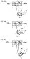
- Poliervorrichtung gemäß Anspruch 7, wobei die Schwingbewegung des Polierkopfes (42) eine Drehung des Polierkopfes (42) in einer Richtung im Uhrzeigersinn und einer Richtung entgegen dem Uhrzeigersinn abwechselnd um den gleichen Winkel von einer Bezugslinie umfasst, die die Mittelachse der Verbindungswelle (67) und einer Mittelachse der Tragwelle (90) rechtwinklig schneidet.
- Ein Polierverfahren zum Polieren eines Umfangs eines Substrats unter Verwendung einer Poliervorrichtung gemäß einem der Ansprüche 1 bis 8, wobei das Verfahren Folgendes aufweist:Vorsehen einer Relativbewegung zwischen einem Polierband (41) unddem Substrat;Halten des Substrats;in Kontakt bringen des Polierbandes (41) durch den Polierkopf (42) mit dem Umfang des Substrats, während das Polierband (41) von der Versorgungsspule (45a) zum Polierkopf (42) transportiert wird; undSchwingen des Polierkopfs (42) um zu bewirken, dass das Polierband (41) um den Schwenkpunkt oszilliert, und zwar während des Kontakts des Umfangs des Substrats.
- Polierverfahren gemäß Anspruch 9, wobei das Polierband (41) sich von der Versorgungsspule (45a) zu dem Substrat über einen Schwenkpunkt der Schwingbewegung des Polierkopfes (42) erstreckt.
- Polierverfahren gemäß Anspruch 9 oder 10, wobei ein Schwenkpunkt der Schwingbewegung in dem Polierkopf (42) positioniert ist.
- Polierverfahren gemäß einem der Ansprüche 9 bis 11, wobei Folgendes vorgesehen ist:das Substrat weist einen Halbleiterwafer auf oder ist ein Halbleiterwafer und zwar mit einem Nutenteil, gebildet im Umfang desselben; undin Kontakt bringen des Polierbandes (41) durch den Polierkopf (42) mit dem Umfang des Substrats, wobei das Polierband (41) durch den Polierkopf (42) mit dem Nutenteil in Kontakt gebracht wird.
- Polierverfahren gemäß einem der Ansprüche 9 bis 12, wobei ferner vorgesehen ist, dass während des Schwingens oder der Schwenkbewegung des Polierkopfes (42) der Polierkopf (42) bezüglich einer Oberfläche des Substrats gekippt wird.
Applications Claiming Priority (1)
| Application Number | Priority Date | Filing Date | Title |
|---|---|---|---|
| JP2007171959 | 2007-06-29 |
Publications (2)
| Publication Number | Publication Date |
|---|---|
| EP2008769A1 EP2008769A1 (de) | 2008-12-31 |
| EP2008769B1 true EP2008769B1 (de) | 2011-03-02 |
Family
ID=39816648
Family Applications (1)
| Application Number | Title | Priority Date | Filing Date |
|---|---|---|---|
| EP08011343A Active EP2008769B1 (de) | 2007-06-29 | 2008-06-23 | Poliervorrichtung und Polierverfahren |
Country Status (7)
| Country | Link |
|---|---|
| US (1) | US7976361B2 (de) |
| EP (1) | EP2008769B1 (de) |
| JP (2) | JP5188285B2 (de) |
| KR (1) | KR101488993B1 (de) |
| CN (1) | CN101332580B (de) |
| DE (1) | DE602008005211D1 (de) |
| TW (1) | TWI436852B (de) |
Families Citing this family (21)
| Publication number | Priority date | Publication date | Assignee | Title |
|---|---|---|---|---|
| US20110081839A1 (en) * | 2009-10-06 | 2011-04-07 | Apple Inc. | Method and apparatus for polishing a curved edge |
| US8892238B2 (en) * | 2009-10-06 | 2014-11-18 | Edward T. Sweet | Edge break details and processing |
| CN101934489B (zh) * | 2010-07-30 | 2012-10-03 | 溧阳市四方不锈钢制品有限公司 | 管坯焊缝打磨机 |
| JP5649417B2 (ja) * | 2010-11-26 | 2015-01-07 | 株式会社荏原製作所 | 固定砥粒を有する研磨テープを用いた基板の研磨方法 |
| US8540551B2 (en) * | 2010-12-15 | 2013-09-24 | Corning Incorporated | Glass edge finish system, belt assembly, and method for using same |
| CN102233536A (zh) * | 2011-05-10 | 2011-11-09 | 淄博隆嘉工贸有限公司 | 陶瓷手模自动抛光机 |
| TWI663025B (zh) * | 2012-09-24 | 2019-06-21 | 日商荏原製作所股份有限公司 | 研磨方法及研磨裝置 |
| US9339912B2 (en) | 2013-01-31 | 2016-05-17 | Taiwan Semiconductor Manufacturing Company, Ltd. | Wafer polishing tool using abrasive tape |
| JP6071611B2 (ja) * | 2013-02-13 | 2017-02-01 | Mipox株式会社 | オリエンテーションフラット等切り欠き部を有する、結晶材料から成るウエハの周縁を、研磨テープを使用して研磨することにより円形ウエハを製造する方法 |
| JP2015000451A (ja) * | 2013-06-17 | 2015-01-05 | ワイエイシイ株式会社 | 基板表面加工装置 |
| JP6113624B2 (ja) * | 2013-10-11 | 2017-04-12 | 株式会社荏原製作所 | 基板処理装置および基板処理方法 |
| CN105196140B (zh) * | 2015-10-20 | 2017-05-31 | 慈溪市华表机械有限公司 | 一种外圆超精机 |
| EP3335832B1 (de) * | 2016-12-15 | 2021-02-03 | Ebara Corporation | Poliervorrichtung und presskissen für presspolierwerkzeug |
| JP6920849B2 (ja) * | 2017-03-27 | 2021-08-18 | 株式会社荏原製作所 | 基板処理方法および装置 |
| JP6974067B2 (ja) * | 2017-08-17 | 2021-12-01 | 株式会社荏原製作所 | 基板を研磨する方法および装置 |
| JP7129166B2 (ja) * | 2018-01-11 | 2022-09-01 | 株式会社荏原製作所 | 基板処理装置及び制御方法 |
| JP7226711B2 (ja) * | 2019-02-28 | 2023-02-21 | 範多機械株式会社 | 斫り装置 |
| CN110405587B (zh) * | 2019-07-29 | 2024-12-24 | 周口市超越科技电子有限公司 | 一种马达电枢自动抛光机 |
| CN111745504B (zh) * | 2020-05-20 | 2022-06-21 | 深圳市裕展精密科技有限公司 | 打磨机构、打磨装置及打磨方法 |
| CN111941201B (zh) * | 2020-08-21 | 2021-12-07 | 许昌学院 | 一种用于法布里-珀罗干涉仪镜板的高精度制造装置 |
| CN114619338B (zh) * | 2022-03-28 | 2024-11-15 | 南通市睿联环保设备有限公司 | 一种扫地车液压杆生产装置 |
Family Cites Families (20)
| Publication number | Priority date | Publication date | Assignee | Title |
|---|---|---|---|---|
| JP2837342B2 (ja) * | 1993-12-13 | 1998-12-16 | 日本ミクロコーティング株式会社 | 研磨装置 |
| JP3081140B2 (ja) | 1995-09-21 | 2000-08-28 | 日本ミクロコーティング株式会社 | 研磨テープによる研磨装置 |
| NO306765B1 (no) * | 1998-04-03 | 1999-12-20 | Grobi As | Anordning for kantrunding av hull i et arbeidsstykke |
| US6685539B1 (en) * | 1999-08-24 | 2004-02-03 | Ricoh Company, Ltd. | Processing tool, method of producing tool, processing method and processing apparatus |
| US6629875B2 (en) * | 2000-01-28 | 2003-10-07 | Accretech Usa, Inc. | Machine for grinding-polishing of a water edge |
| JP4156200B2 (ja) * | 2001-01-09 | 2008-09-24 | 株式会社荏原製作所 | 研磨装置及び研磨方法 |
| JP2003220546A (ja) * | 2002-01-24 | 2003-08-05 | Soken Kogyo Kk | ベルト式研磨装置 |
| JP4090247B2 (ja) * | 2002-02-12 | 2008-05-28 | 株式会社荏原製作所 | 基板処理装置 |
| JP4125148B2 (ja) | 2003-02-03 | 2008-07-30 | 株式会社荏原製作所 | 基板処理装置 |
| CN100429752C (zh) * | 2004-02-25 | 2008-10-29 | 株式会社荏原制作所 | 抛光装置和衬底处理装置 |
| EP1810321B1 (de) * | 2004-10-15 | 2014-01-01 | Ebara Corporation | Poliervorrichtung und polierverfahren |
| JP2006142388A (ja) * | 2004-11-16 | 2006-06-08 | Nihon Micro Coating Co Ltd | 研磨テープ及び方法 |
| US20090017733A1 (en) * | 2005-04-19 | 2009-01-15 | Ebara Corporation | Substrate processing apparatus |
| EP1872392B1 (de) * | 2005-04-19 | 2012-02-22 | Ebara Corporation | Substratverarbeitungsvorrichtung |
| JP5196709B2 (ja) * | 2005-04-19 | 2013-05-15 | 株式会社荏原製作所 | 半導体ウエハ周縁研磨装置及び方法 |
| US7993485B2 (en) * | 2005-12-09 | 2011-08-09 | Applied Materials, Inc. | Methods and apparatus for processing a substrate |
| EP1976806A4 (de) * | 2005-12-09 | 2011-08-10 | Applied Materials Inc | Verfahren und vorrichtung zur verarbeitung eines substrats |
| WO2007126815A2 (en) * | 2006-03-30 | 2007-11-08 | Applied Materials, Inc. | Methods and apparatus for polishing an edge of a subtrate |
| JP2008036783A (ja) * | 2006-08-08 | 2008-02-21 | Sony Corp | 研磨方法および研磨装置 |
| JP2008284684A (ja) * | 2007-05-21 | 2008-11-27 | Applied Materials Inc | 研磨アームを使用して基板の縁部を研磨する方法及び装置 |
-
2008
- 2008-06-16 US US12/213,186 patent/US7976361B2/en active Active
- 2008-06-19 JP JP2008160380A patent/JP5188285B2/ja active Active
- 2008-06-19 TW TW097122820A patent/TWI436852B/zh active
- 2008-06-23 DE DE602008005211T patent/DE602008005211D1/de active Active
- 2008-06-23 EP EP08011343A patent/EP2008769B1/de active Active
- 2008-06-27 CN CN2008101285883A patent/CN101332580B/zh active Active
- 2008-06-27 KR KR20080061705A patent/KR101488993B1/ko active Active
-
2012
- 2012-12-14 JP JP2012273699A patent/JP5525590B2/ja active Active
Also Published As
| Publication number | Publication date |
|---|---|
| TWI436852B (zh) | 2014-05-11 |
| JP5188285B2 (ja) | 2013-04-24 |
| CN101332580B (zh) | 2012-05-09 |
| KR20090004590A (ko) | 2009-01-12 |
| DE602008005211D1 (de) | 2011-04-14 |
| EP2008769A1 (de) | 2008-12-31 |
| TW200932423A (en) | 2009-08-01 |
| US7976361B2 (en) | 2011-07-12 |
| KR101488993B1 (ko) | 2015-02-02 |
| CN101332580A (zh) | 2008-12-31 |
| JP2013075358A (ja) | 2013-04-25 |
| US20090004952A1 (en) | 2009-01-01 |
| JP2009028892A (ja) | 2009-02-12 |
| JP5525590B2 (ja) | 2014-06-18 |
Similar Documents
| Publication | Publication Date | Title |
|---|---|---|
| EP2008769B1 (de) | Poliervorrichtung und Polierverfahren | |
| CN102941530B (zh) | 抛光方法和基片 | |
| US9457447B2 (en) | Polishing apparatus and polishing method | |
| EP2502701B1 (de) | Poliervorrichtung und Polierverfahren | |
| US8393935B2 (en) | Polishing apparatus | |
| TWI820076B (zh) | 基板處理裝置以及控制方法 | |
| US20080293334A1 (en) | Methods and apparatus for using a bevel polishing head with an efficient tape routing arrangement | |
| US10414013B2 (en) | Polishing method and polishing apparatus | |
| US6638147B2 (en) | Polishing method for removing corner material from a semi-conductor wafer | |
| TWI433754B (zh) | 研磨裝置 | |
| JP7296864B2 (ja) | 研磨装置および研磨方法 | |
| JP3888618B2 (ja) | ロッド端面加工装置 | |
| JP3542815B2 (ja) | ウェハーノッチ部の鏡面研磨装置およびその鏡面研磨方法 | |
| JPH0724720A (ja) | 両端軸状部研磨装置 | |
| US20250178150A1 (en) | Substrate polishing method | |
| WO2009011408A1 (ja) | 研磨装置 | |
| KR200208032Y1 (ko) | 리니어 모션가이드가 설치된 초정밀 연마기 | |
| JP2003007657A (ja) | ウェハノッチの鏡面研磨装置及び鏡面研磨方法 |
Legal Events
| Date | Code | Title | Description |
|---|---|---|---|
| PUAI | Public reference made under article 153(3) epc to a published international application that has entered the european phase |
Free format text: ORIGINAL CODE: 0009012 |
|
| AK | Designated contracting states |
Kind code of ref document: A1 Designated state(s): AT BE BG CH CY CZ DE DK EE ES FI FR GB GR HR HU IE IS IT LI LT LU LV MC MT NL NO PL PT RO SE SI SK TR |
|
| AX | Request for extension of the european patent |
Extension state: AL BA MK RS |
|
| 17P | Request for examination filed |
Effective date: 20090624 |
|
| 17Q | First examination report despatched |
Effective date: 20090722 |
|
| AKX | Designation fees paid |
Designated state(s): DE |
|
| GRAP | Despatch of communication of intention to grant a patent |
Free format text: ORIGINAL CODE: EPIDOSNIGR1 |
|
| GRAS | Grant fee paid |
Free format text: ORIGINAL CODE: EPIDOSNIGR3 |
|
| GRAA | (expected) grant |
Free format text: ORIGINAL CODE: 0009210 |
|
| AK | Designated contracting states |
Kind code of ref document: B1 Designated state(s): DE |
|
| REF | Corresponds to: |
Ref document number: 602008005211 Country of ref document: DE Date of ref document: 20110414 Kind code of ref document: P |
|
| REG | Reference to a national code |
Ref country code: DE Ref legal event code: R096 Ref document number: 602008005211 Country of ref document: DE Effective date: 20110414 |
|
| PLBE | No opposition filed within time limit |
Free format text: ORIGINAL CODE: 0009261 |
|
| STAA | Information on the status of an ep patent application or granted ep patent |
Free format text: STATUS: NO OPPOSITION FILED WITHIN TIME LIMIT |
|
| 26N | No opposition filed |
Effective date: 20111205 |
|
| REG | Reference to a national code |
Ref country code: DE Ref legal event code: R097 Ref document number: 602008005211 Country of ref document: DE Effective date: 20111205 |
|
| P01 | Opt-out of the competence of the unified patent court (upc) registered |
Effective date: 20230517 |
|
| PGFP | Annual fee paid to national office [announced via postgrant information from national office to epo] |
Ref country code: DE Payment date: 20250429 Year of fee payment: 18 |